

Abstract
An improved method of average channel temperature and channel temperature profile determination is introduced in this paper applied to AlGaN/GaN HEMT using quasi-static I–V characterization and external heater. Particular HEMT resistances and threshold voltage were experimentally determined at different ambient temperatures from TLM measurements, HEMT output and transfer I–V characteristics. Negligible pinch-off area and leakage current dependence on drain voltage allows to obtain average temperature ∼77 °C for dissipated power 1.5 W using simple recurrent differential calculations. The HEMT channel temperature profile exhibiting maximum peripheral temperature ∼130 °C for dissipated power 1.5 W was simulated and verified utilizing the device electrical parameters variation.
Export citation and abstract BibTeX RIS
1. Introduction
The advanced GaN-based devices are promising to use in high temperature, frequency, power and microwave applications. However, the high potential of these devices is deteriorated by self-heating during the operation. This influences the electrical characteristics as well as device reliability [1–3], the temperature is a key factor here. High thermal conductance of particular materials, especially substrates, plays a significant role in the heat distribution. Power devices prepared on SiC and Si substrates exhibit better heat distribution than the ones grown on sapphire substrate [4].
Various experimental methods essential for complex characterization were developed to determine the channel temperature of power GaN-based the high electron mobility transistor (HEMT), e.g. Raman spectroscopy or interferometric mapping [5–7]. These techniques are widely applied though some measurements require advanced setup or assemblies to obtain accurate results. Thermal simulations explain thermally induced effects inside the structure in symbiosis with experimental data.
In this work an alternative method to [8] is described in the theoretical part and subsequently utilized for quasi-static I–V characterization with the consecutive analysis to determine the HEMT channel temperature coming out from field-effect transistor (FET) behavioral model. The experimental part of this work is focused on AlGaN/GaN HEMT average temperature and thermal profile determination.
2. Theory
2.1. Differential FET behavioural model
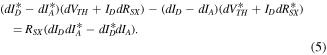
Lateral FET consists of the gated core FET area, ungated and ohmic contact source/drain area as shown in figure 1. The total FET resistance is the sum of the core FET channel resistance RCH in the length dG, source to gate channel resistance RS in the length dS, drain to gate channel resistance RD in the length dD and source/drain ohmic contact resistances RCS, RCD in the transfer length dCS, dCD. In saturation regime pinch-off area of voltage drop VPO is formed nearby the drain-side gate edge at x ∈ (–dPO, 0) under the gate as well as at x ∈ (0, dPD) in the drain to gate gap. For quasi-static operation the difference between investigated FET gate voltage VGS, drain voltage VDS and core FET gate voltage VGO, drain voltage VDO, respectively, is given by the voltage drop caused by resistances RS, RD, RCS, RCD at drain current ID:


Figure 1. A cross-sectional view of lateral FET. Reprinted from [8]. The origin is positioned in the middle of the drain-side gate edge.
Download figure:
Standard image High-resolution imageCore FET behavioural model [8] coming out from core FET functional approximation  [9] results in core FET transconductance gGO =
  Further substitution
  and
and 
 leads to:

Utilizing [8] dIA involves output conductance gDO = dID/dVDO and thermal coefficient determined partially by threshold voltage VTH change, channel concentration n shift, carrier velocity v and carrier mobility μ = v/EX change caused by temperature T change having an impact on horizontal and vertical electric field (EX and EZ).
External heater utilization causes small temperature increase dT*(x) across the structure resulting in current change dID* and dIA* addicted to dRSX* and dVTH*:

If both (3) and (4) are linearly independent and constant VGS, VGS* are supposed then (4) divided by (3) results in:
Leakage current path allocation with respect to thermal gradient is requisite for proper calculations mentioned in [8].
2.2. Threshold voltage and source/drain/contact resistance determination
Temperature dependence of threshold voltage VTH and particular resistances RS, RD, RCS, RCD are crucial for FET channel temperature determination [10]. RS(0), RD(0), RCS(0), RCD(0) at low ID are lower than RS(ID), RD(ID), RCS(ID), RCD(ID) used in (1), (2) or (5) due to finite current saturation level [11]. Therefore particular correction factors rS = RS(ID)/RS(0), rD = RD(ID)/RD(0), rCS = RCS(ID)/RCS(0), rCD = RCD(ID)/RCD(0) at ID and T are requisite.
Relative small rS, rD, rCS, rCD change allows correction of RS, RD, RCS, RCD and dRS, dRD, dRCS, dRCD in simple multiplication way and usually rS ≈ rD, rCS ≈ rCD. In general RS(ID), RD(ID), RCS(ID), RCD(ID) and ID change cause relative resistance drop demonstrated for RS(ID):

whereas rS depends on both ID and T and RS(0) on T only dRS(ID) is a linear combination of dID and dT.
Thermal dependence of VTH(0) and particular thermal coefficient kVTH(0) = dVTH(0)/dT are typically acquired from transfer low power I–V characteristics [12–14]. Under quasi-static condition dVTH(ID) = rVTHdVTH(0) is supposed ID dependent only using correction factor rVTH in core FET functional approximation 
Low power output I–V characteristics at defined T allow to determine RS(0), RD(0), RCS(0), RCD(0) temperature dependencies and calculate particular thermal coefficients kRS(0) = dRS(0)/dT, kRD(0) = dRD(0)/dT, kRCS(0) = dRCS(0)/dT, kRCD(0) = dRCD(0)/dT [8]. In the case of channel thermal gradient those coefficients in symbiosis with correction factors determine the temperature dependence of channel resistance per length.
2.3. Average channel temperature evaluation
Under the quasi-static condition an average temperature TA along the whole channel is assumed. This hypothetic situation is demonstrated by infinite channel thermal conductance in the FET of width w and length dS + dG + dD. Therefore power density distribution in the channel plays no role. Differential FET behavioral model offers TA determination utilizing core FET thermal coefficient  and substitution
  Dissipated power change
  results in dTA. Ambient temperature T0 increase dT0* caused by the external heater is set before measurement. Therefore active area temperature increase
  at the device operation consists of the active area temperature change
  at constant dissipated power and
  caused by dissipated power difference
  at constant VDS utilizing differential thermal resistance
  Substitution
  yields:

It is advisable to calculate dTA for each operating point, however  invoked by dT0* depends on TA. Therefore dTA caused by defined dP is possible to be obtained for varying T0 across the operating TA range assuming
  ≈ dT0* [13].
Dissipated power change and thermal parameters are used in (7) whereas electrical parameters utilizing ID and TA dependence of RSX and VTH substituted in (5) lead to kA determination and the following solutions:
- (1)
- (2)Thermal coefficients kRSX(ID) = rSkRS(0) + rCSkRCS(0), kRDX(ID) = rDkRD(0) + rCDkRCD(0) are possible to be obtained at operating ID and TA for relatively small rS, rD, rCS, rCD, rVTH variation. Considering gDO determined by pinch-off area and leakage current modulation caused by dVDO, substitution
 in (5) yields:


Recurrent calculations coming out from (7) and (9) allow to obtain dTA incrementing TA and utilizing  from the previous operating point. Zero a and RSX causing zero dVGO result in solution similar to (8) where the term
  is replaced by
  Substitution of dVDO by dVPO and dVDS using a differential form of (2) and leakage current are recommended to be incorporated in (9).
Negligible leakage current and dVTH ≪ dVPO yields dVPO ≈ dVDO and  where ddPO is dPO change with VPO whereas thermal dPO change is included in kGC [8]. If
 ![$d[{R}_{SX}({I}_{D}){I}_{D}]+d[{R}_{DX}({I}_{D}){I}_{D}]\langle \langle d{V}_{DS}$](https://content.cld.iop.org/journals/0268-1242/35/2/025006/revision2/sstab5d85ieqn26.gif) then condition dVPO ≈ dVDO ≈ dVDS is satisfied. The condition
then condition dVPO ≈ dVDO ≈ dVDS is satisfied. The condition  for TA close to T0 is used for the temperature assumption in the linear regime area [8].
2.4. Channel temperature profile evaluation
Temperature profile evaluation for a device under quasi-static condition takes thermal gradient along the channel and temperature dependent thermal conductance into account. An uniform power dissipation density is assumed along z ∈ (dCH–hCH/2, dCH + hCH/2) using average channel depth dCH and vertical width hCH. Constant power density and temperature consideration along y ∈ (–w/2, +w/2) for x-position are requisite to define channel temperature T(x) and resistance element per length Ri(x) [8]. Power density per length Pi(x) = Ri(x)ID2 = IDEX(x) = IDdVCH(x)/dx where EX(x) and VCH(x) = EX(x)dx are the channel electric field and potential, respectively. In the ungated source and drain area EX(x) is distorted by Ri(x) modulation due to self-heating. Because of thermal gradient in the structure RS and RD at ID are declared in a way shown for RS:

Assuming small dCS and dCD both dRCS and dRCD at ID are defined in a way shown for dRCD:
The core FET acts as the sum of elementary FETs of transconductance gGO(x) and length dx. Current continuity equation is partially satisfied for ID change caused by dVTH(x) and ddPO resulting in VCH(x) bending. Similarly kGC(x) is advised to be calculated at appropriate x ∈ (–dG, –dPO) using Poisson and current continuity equation and taking n, v, EX and EZ variation into account. Those calculations specific for each FET type allow to obtain core FET average dVTH. Although simple dVTH approximation is advised to be applied for short channel FET or for 

Temperature profile evaluation based on simple iterations is described in [8]. For simple temperature estimation in the saturation regime to avoid the iteration process total dissipated power increase  is supposed as uniform pinch-off area power dissipation contribution with respect to rising dPO and dPD. Pinch-off area dimensions dPO, dPD, hCH affect T(x) significantly inside this area whereas farther those parameters become less dominant.
Temperature change  caused by dT0* such as
  invoked by uniform dissipated power change along the active area
  are possible to be acquired by thermal simulations giving opportunity to assume dT*(x) in a simple way:

Differential correction factor kT as ratio between simulated and calculated dT(x) gives opportunity to compare results obtained by simulations and calculated from experimentally acquired electrical FET attributes using differential FET behavioral model. Inaccurate assumption of particular thermal conductance, leakage current paths or power density cause kT deviation from one. In that case self-heating in entire channel area is advised to be considered or more proper electrical and thermal model to be employed. Differential equations are suitable to be replaced by difference formulas in numerical recurrent calculations.
Mentioned procedure is allowed to be used for for multi-gated FET as well. In the case of symmetric double gated structure drain current under each gate is ~ID/2. Self-heating plays role in a different non-uniform ID distribution for multi-gated FET, VCH(x) boundary conditions are useful here.
3. Experimental
3.1. Structure design and experimental setup
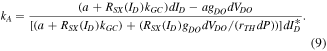
The investigated Al0.29Ga0.71N/GaN HEMT structure including 1.5 nm GaN/14.5 nm Al0.29Ga0.71N/50 nm undoped GaN/1650 nm GaN heterostructure was grown by MOVPE on 500 μm thick 4H-SiC substrate. The backside Au contact is soldered to 1 mm thick CuMo leadframe by 60 μm thick AuSn solder. Top ohmic drain/source and gate contacts were prepared by standard Au-based metallization. Horizontal view of investigated GTLM HEMT of w ≈ 125 μm, dG ≈ 1 μm, dS ≈ dD ≈ 5 μm and source/drain ohmic contact length ∼100 μm is shown in figure 2. The device is set in the package open from top, placed on the Al thermal chuck preserved at a constant temperature.
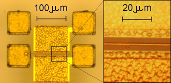
Figure 2. Horizontal view of GTLM HEMT structure.
Download figure:
Standard image High-resolution imageThe output and transfer I–V characteristics were measured using semiconductor parameter analyzer Agilent 4155C and controlled thermal chuck. To obtain ID dependence zero gate voltage VGS was kept while drain voltage VDS varied from 0 up to 40 V. The parameters RS and VTH were acquired from the output and transfer I–V characteristics measured in low power regime at temperature range 25 °C–120 °C, respectively. The device was recovered by one minute white LED illumination between measurements. 3D thermal finite element method (FEM) simulations of the device were performed by Synopsys TCAD Sentaurus coming out from thermal conductivity values shown in table 1 [15, 16].
Table 1. Temperature dependence of thermal conductivity values utilized in 3D thermal FEM simulations.
| Material | Thermal conductivity (W m−1 K−1) | |
|---|---|---|
| Au | 310 | |
| AlGaN | 40 × (T/298)−1.37 | |
| GaN (C doped) | 190 × (T/298)−1.37 | |
| 4H-SiC | xy-axis | 370 × (T/298)−1.5 |
| z-axis | 430 × (T/298)−1.5 | |
| AuSn | 57 | |
| CuMo | 160 | |
3.2. Average channel temperature and temperature profile determination
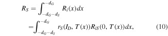
Linearization of RS(0) and VTH(0) temperature dependence depicted in figure 3 results in RiS(0) ≈ RiD(0) ≈ 4.14 Ω μm−1 at 25 °C, kRS(0) ≈ kRD(0) ≈ 29.4 mΩ K−1 μm−1, kVTH(0) ≈ 1.46 mV K−1 assuming rVTH ≈ 1. From transmission line measurements (TLM) correction coefficients rS ≈ rD ≈ 1+kDID, kD ≈ 6 A−1 for RiS, RiD at operating temperature and the current range was obtained using FEM simulations to eliminate self-heating part. Constant RCS ≈ RCD ≈1.2 Ω and rCS ≈ rCD ≈ 1 were verified. Transfer I–V characteristics point on low leakage current.

Figure 3. Measured RiS(0) and VTH temperature dependence.
Download figure:
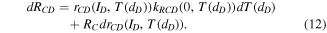
Standard image High-resolution imageThe measured ID dependence on VDS for VGS = 0 V at T0 = 25 °C and 35 °C exhibiting ΔT* = 10 °C and ΔID* are shown in figure 4. Additionally, nearly constant dPO/VPO ≈ 0.6 nm V−1 and dPD/VPO ≈ 3 nm V−1 were obtained from electro-thermal model. HEMT channel temperature profile shown in figure 5 was obtained using heat flow injector [8] in 3D thermal FEM simulations. Utilizing An ≈ 0.15 the relative saturation velocity change ![${v}_{SAT}(T)/{v}_{SAT}\,=-T/[T+1700\,{\rm{K}}]$](https://content.cld.iop.org/journals/0268-1242/35/2/025006/revision2/sstab5d85ieqn33.gif) was assumed.
was assumed.
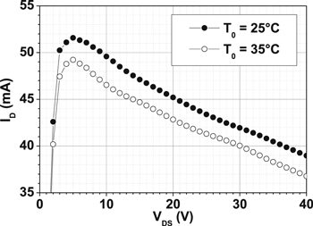
Figure 4. Output I–V characteristics at VGS = 0 V for various temperature.
Download figure:
Standard image High-resolution image
Figure 5. Channel temperature profile for various dissipated power.
Download figure:
Standard image High-resolution imageSimulated average temperature of the ungated source area, gate area and peripheral temperature of the pinch-off area exhibit linear dependence on dissipated power therefore the condition  is satisfied reducing the external heater requirements on the small temperature increase only utilizing ΔT0* stabilization unaffected by ΔP and ΔP*.
An average temperature TA shown in figure 6 was calculated using (8) neglecting dPO. Considering dPO slightly higher TA was obtained solving (7) and (9) incorporating  and
and  and. Calculated TA is close to simulated average temperature of ungated source area pointing on major thermal RS and minor VTH and vSAT change.

Figure 6. Calculated TA and FEM simulated particular average temperature dependence on dissipated power P.
Download figure:
Standard image High-resolution imageFinite small ΔID* and ΔT0* caused by external heater takes effect on finite point differential analysis deviation resulting in correct TA determination.
Simulated channel temperature profile TSIM(x) at T0 and  for various dissipated power was obtained. In the case of temperature independent kVTH(0), kRS(0) ≈ kRD(0) and zero kRCS(0) ≈ kRCD(0) average temperature difference values of ungated source area ΔTARS and gated area ΔTACH are requisite for ΔRS determination and for simple ΔVTH approximation (13):


Utilization of (14), (15) and (16) leads to ΔT*ARS, ΔT*ACH and ΔT*(–dPO) acquisition. Polynomial approximation of ΔTARS, ΔTACH, ΔT(–dPO) and ΔT*ARS, ΔT*ACH, ΔT*(–dPO) allows to acquire those parameters for each operating point.
Accurate kGC(x) and gDO(x) determination requires calculations based on Poisson and current continuity equation taking channel thermal gradient into account. To avoid this VCH(x) bending caused by ΔdPO and  due to
  are supposed resulting in
  Because of negligible thermal 2DEG concentration change in AlGaN/GaN channel carrier velocity variation is the determining factor. For small VCH(x) thermal bending excluding VTH(x) thermal change current continuity equation results in
  for x ∈ (–dG, –dPO), n(x) includes built-in such as EZ induced carrier concentration, gate boundaries exhibit ΔT(–dPO) > ΔT(–dG), EX(–dPO) ≫ EX(–dG), ΔT(–dPO) > ΔT(–dG). Assuming acceptable deviation in
  and ΔvSAT minor impact on ΔID in comparison with ΔRSX the formula
  is found to be sufficient approximation [8].
The ratio between calculated ΔT(x) and simulated ΔTSIM(x) temperature change  applied in (5) allows to compare simulated and calculated thermal profile in a multiplication way for ΔP applied for simulated ΔTARS, ΔTACH, ΔT(–dPO). Values ΔT*ARS, ΔT**ACH, ΔT*(–dPO) are supposed as simulated using (14). Preliminarily calculated parameters RSX(ID), gDO, kRS(ID), kRD(ID), kVTH(ID), kGC(–dPO) for defined operating point and relatively small rS, rD, rVTH variation allow (5) to be transformed into the following difference equation to calculate kT:
Channel temperature TSAT(x) obtained from simulations at saturation voltage is used as initial parameter for recurrent calculations. Therefore the resultant temperature in the saturation regime is yielded as:

Obtained kT is shown in figure 7, particular simulated and calculated average temperature TARS, TACH such as T(−dPO) are compared in figure 8.
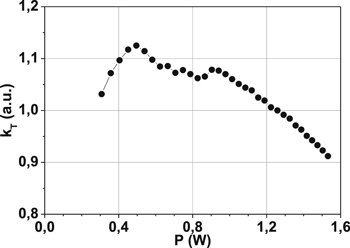
Figure 7. Correction factor versus dissipated power.
Download figure:
Standard image High-resolution image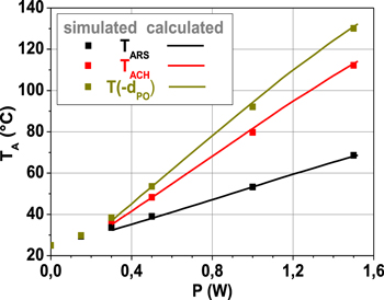
Figure 8. Particular average temperature versus dissipated power (calculated and FEM simulated).
Download figure:
Standard image High-resolution image
Maximal peripheral temperature T ≈ 130 °C was reached for P = 1.5 W, however channel temperature is higher inside pinch-off area depending on dPO, dPD, and hCH. Although kT deviation is ∼12% a good correspondence between thermal simulations and calculations using (17) was achieved.
4. Conclusions
The aim of this work was to determine the average HEMT channel temperature and to verify the simulated channel profile utilizing an external heater together with electrical parameters acquired from quasi-static measurements. Lateral FET behavioral model was employed in recurrent differential calculations. Average channel temperature TA ≈ 77 °C was calculated for dissipated power P = 1.5 W in power Al0.29Ga0.71N/GaN HEMT structure grown on SiC substrate. Calculated TA close to the average temperature of ungated source area hints the significant thermal RS change. Moreover, simulated channel temperature profile exhibiting maximum peripheral temperature T ≈ 130 °C for dissipated power P = 1.5 W was verified using experimentally achieved electrical parameters.
Acknowledgments
The research leading to these results has received funding from the Electronic Component Systems for European Leadership Joint Undertaking under grant agreement No. 662322, project OSIRIS. This Joint Undertaking receives support from the European Union's Horizon 2020 research and innovation program, France, Norway, Slovakia and Sweden. This publication reflects only the author's view and the JU is not responsible for any use that may be made of the information it contains. The work was also supported by Grant VEGA 1/0739/16 through the Ministry of Education, Science, Research and Sport of Slovakia.