
Abstract
While recent work developing GaAsBi for opto-electronic applications has shown promise, it has also indicated that the large valence band offset of GaAsBi/GaAs may cause undesirable hole-trapping in GaAsBi quantum wells. In this work, hole-trapping is demonstrated to be the cause of the reduced depletion width of GaAsBi/GaAs multi-quantum well solar cell devices under illumination. Modelling of the quantum confinement energies in these devices shows how the carrier escape times vary as functions of temperature, providing a tool for the design for future GaAsBi based photovoltaic devices.
Export citation and abstract BibTeX RIS

Original content from this work may be used under the terms of the Creative Commons Attribution 3.0 licence. Any further distribution of this work must maintain attribution to the author(s) and the title of the work, journal citation and DOI.
Introduction
A recent report on GaAsBi based multiple quantum well (MQW) p–i–n diodes suggested that they suffered from incomplete photo-excited carrier extraction [1]. The mechanism responsible for this effect is identified in this paper.
MQW solar cells were first proposed by Barnham and Duggan in [2]. After significant research and the introduction of strain balancing [3], the MQW design has produced commercially available triple-junction solar cells with median efficiencies above 41% at 500× concentration [4]. Development of MQW solar cells is still ongoing [5]; however, the success of InGaAs MQW solar cells has been limited by the critical thickness of individual InGaAs quantum wells (QWs). In order for InGaAs QWs to absorb light at 1 eV, they must be produced very close to their critical thickness, which limits their reliability and commercial yield. For MQW photovoltaics (PV) to develop, alternative alloys must be identified to reach longer wavelengths.
Highly mismatched alloys (HMAs) have emerged over recent years as potential candidates for many opto-electronic applications. For example, the incorporation of N into GaAs produces a band gap reduction in excess of ∼130 meV/% N at low compositions [6], most of which is due to a downward shift in the conduction band edge. This is very large compared to the reduction of ∼20 meV/% In [7]. Despite degradation in the material quality of GaAsN even at small N fractions [8], a dilute nitride containing solar cell recorded an efficiency of 44% in 2012 [9]. Another candidate HMA is GaAsBi, with a band gap reduction of around 80 meV/% Bi [10]. Together with an increase in the spin–orbit split off energy, this has indicated its potential for devices such as solar cells [11], lasers [12], and detectors [13].
Recently, the photovoltaic performance of a series of GaAsBi/GaAs MQW p–i–n diodes was investigated [1]. The results showed that strained GaAsBi MQWs can provide a comparable absorption edge to state-of-the-art, strain-balanced, interlayered InGaAs/GaAsP [5] devices. However, two issues were observed with the GaAsBi devices: firstly, the onset of spectral absorption was gradual, limiting the voltage of the devices; secondly, the quantum efficiency of the GaAsBi above the absorption edge was lower than expected, despite dark capacitance–voltage measurements indicating near full depletion of the device i-regions.
A possible explanation for this effect is a charging of the MQW i-region as observed by Professor Naçi Balkan and co-workers. In 2012 Khalil et al [14] demonstrated stepped changes in the bias dependent photoluminescence (PL) and photocurrent (PC) signals from a GaInNAs MQW device at low temperature. They calculated that, due to the large conduction band offset in dilute nitride materials, the room temperature escape time for electrons in the QW ground state was over three orders of magnitude larger than that for holes; this disparity increased to well over eight orders of magnitude at low temperatures. This disparity means that the holes were able to escape the QWs, while the electrons (with no holes with which to recombine) accumulated in the QWs. The accumulation of electrons charges the i-region and screens the electric field, confining the depletion region between the positive n-type region and the negatively charged QWs. Depending on the level of QW charging and applied bias, the depletion region only covers some number of the QWs; varying the bias changes this number. The electron escape time from a QW is dramatically reduced by the application of an electric field, so QWs within the depletion region contribute more strongly to PC and those without contribute more strongly to PL. Thus, as the applied bias is varied and the depletion edge moves past individual QWs, the PL and PC signals show a 'stepped' behaviour. This behaviour was successfully simulated by Royall et al [15], who added further evidence to this explanation by noting that the number of experimentally observed steps corresponds to the number of QWs in a device.
Another explanation for these steps, postulated by the group is that the application of an electric field brings the quantum confined energy levels of adjacent QWs into resonance [16, 17]. However, the observed lack of negative differential resistance from these devices, along with the presence of 'stepped' PC and PL from samples with large (20 nm) barriers, caused this explanation to be abandoned [15].
The effect observed by Professor Balkan et al fundamentally indicates a disparity in the escape rates of different photo-excited carriers within their MQW material. This kind of disparity has been shown to be deleterious to solar cell performance under some circumstances [18], and has been suggested to be of potential benefit under others [19]. By demonstrating this effect—which is most easily observed at low temperature—in the GaAsBi/GaAs MQWs reported in [1], this paper will provide a possible explanation for the lower than expected open circuit voltage and internal quantum efficiency (IQE) of those devices at room temperature.
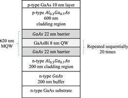
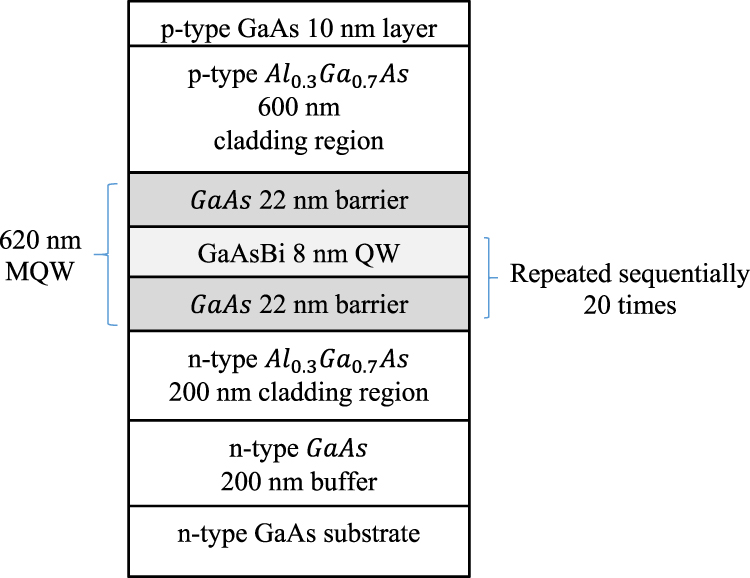
Figure 1. The p–i–n diode design of QW20.
Download figure:
Standard image High-resolution imageMethodology
The GaAsBi MQW p–i–n device used in this work (referred to as QW20) contains a 20 period MQW, which comprises nominally 8 nm GaAsBi QWs and 22 nm GaAs barriers. The full nominal structure is as follows and is illustrated in figure 1.
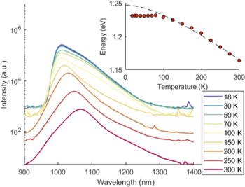
Figure 2. Temperature dependent PL from QW20. The inset shows the temperature dependence of the estimated ground state transition (red points), along with a Varshni curve fitted to the data in the range 100–300 K (dotted line).
Download figure:
Standard image High-resolution imagen-type GaAs substrate; 200 nm n-type GaAs buffer; 200 nm n-type Al0.3Ga0.7As cladding region; 620 nm MQW i-region; 600 nm p-type Al0.3Ga0.7As cladding region; 10 nm p+ GaAs capping layer. The structure was grown by molecular beam epitaxy and details of the growth are discussed elsewhere [20]. Standard epi-ready wafer preparation, outgassing and oxide removal procedures were used. The growth temperatures used were 580 °C for the GaAs and AlGaAs buffer and cladding regions, and 380 °C for the MQW region. The growth rates used were 0.55 μm h−1 for the GaAs and GaAsBi regions, and 0.79 μm h−1 for the AlGaAs regions. The MQW region was grown under a near stoichiometric As4 flux to provide a wider GaAsBi growth window [21]. The rest of the structure was grown using As2.
Transmission electron microscopy (TEM) investigation showed that most of the actual layer thicknesses in this device were less than the nominal thicknesses by about 7% (see QW20 in table 1 in [20]); the QWs, however, were measured to be approximately 40% smaller than their nominal thickness at 4.8 ± 0.3 nm [20]. The TEM investigation also showed that the QWs do not have 'square' Bi profiles and that the first QW grown was not identical to the subsequent QWs. This makes a quantitative estimate of the QW Bi content problematic. An estimate assuming 'square' QWs and based on reconciling the QW/barrier thicknesses with the strain observed by x-ray diffraction measurements and the peak PL signal, arrived at a QW Bi content of 4.4 ± 0.5% and a width of 5.8 ± 0.9 nm [22]. This estimate is in fair agreement with the TEM estimated QW width [20] and the Bi content derived in this paper (5%).
The devices were packaged onto T05 headers for subsequent characterisation.
A 679 nm laser was used as an excitation source for PL measurements. The device temperature was controlled during PL and PC measurements using a closed-cycle He cryostat held under vacuum to prevent issues with condensation at low temperatures. The cryostat was fitted with feedthroughs to allow for electrical contact to the device under vacuum, the PL was dispersed by a monochromator and was detected by a liquid nitrogen-cooled germanium detector. A 660 nm LED was used for light biasing during illuminated current–voltage (IV) (100 K) and capacitance–voltage (CV) (room temperature) measurements; the LED was positioned outside the cryostat and a lens was used to focus the light onto the MQW device. 660 nm was chosen for the measurements to ensure that minimal absorption occurs in the upper AlGaAs cladding region and that electrons and holes are excited throughout the i-region.
CV measurements were undertaken by using an HP LCR metre with a 1 MHz test frequency and IV measurements were undertaken using a Keithley source measure unit. (The CV measurements tested at 100 kHz showed identical results at RT suggesting that there was no trapping problem in this frequency range.)
For reference, the CV measurements were compared to those from a MQW device that contained 65 × 8.3 nm In0.1Ga0.9As QWs with 17.4 nm GaAs0.911P0.089 barriers in its i-region.
The IQE of the device was measured in reverse bias by performing separate external quantum efficiency and reflectance measurements. The device was illuminated by a halogen lamp coupled to a Bentham Instruments monochromator. The resulting monochromatic light was delivered via a 600 μm core optical fibre to a custom-built microscope system, which illuminated a small (150 × 150 μm) area on the device. The incident spectrum was measured using calibrated Si and Ge detectors. For the reflectance (R) measurement, the reflected light was measured using calibrated Si and Ge detectors and the device reflectance extracted from the raw data using corresponding measurements of a reference mirror.
The absorption coefficient of the MQW region was deduced from the IQE using the assumption that there is full carrier extraction under reverse bias [23]
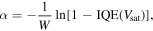
where W is the thickness of the MQW region (620 nm), and Vsat is the reverse bias voltage at which the current saturates (−6 V).
Results
Photoluminescence
The PL from the device is shown in figure 2. The PL is quite broad, with full width at half maximum (FWHM) values between 62 and 90 meV. The FWHM does not vary monotonically with temperature; it peaks between 60 and 70 K and reaches a minimum between 125 and 150 K, which is qualitatively consistent with other reports in the literature [24–26]. At high temperature the PL is dominated by a single peak; however, as the temperature is decreased, a low energy shoulder appears on the spectrum. This shoulder can be explained by the distribution of carriers amongst sub-band gap localised states [27, 28]. The emitted PL was fitted as the sum of three Gaussians. The highest energy Gaussian was assumed to correspond to the ground state transition in the QW and was modelled using the Varshni equation [29], with the fitting parameters 
 and
and  in good agreement with the values reported in [27]. Note that this is assumed to be the temperature dependence of the ground state transition energy (plotted in figure 2 inset), which is a function of the band gap and quantum confinement. The deviation of the experimental data from the fit shows that this approach does not necessarily identify the dominant radiative recombination pathway at low temperatures, but a good fit is obtained at temperatures ≥100 K. The subsequent low temperature measurements are therefore conducted at 100 K in an attempt to simplify the interpretation of the results. Any carriers localised below the band gap on Bi induced states will see a larger potential barrier for escaping to the GaAs band edge; this would also be true in the event that the carriers occupied states at the band edge (i.e. in the absence of quantum confinement).
Capacitance–voltage
Dark and illuminated CV measurements were performed on QW20, alongside the InGaAs/GaAsP reference sample. The CV curves from QW20 and the InGaAs based device are shown in figures 3(a) and 3(b) respectively. A thorough analysis of the CV profiles of these devices has not been attempted; however, the simple plots in figure 3 show a clear difference between the two devices. The InGaAs based device shows a very similar capacitance under dark and illuminated conditions. QW20 shows a significant increase in capacitance under illumination near zero bias. Clearly the depletion width of QW20 is affected by illumination, while this does not appear to be the case for the InGaAs based device.

Figure 3. Room temperature capacitance–voltage measurements from (a) QW20, and (b) a reference InGaAs/GaAsP MQW device.
Download figure:
Standard image High-resolution image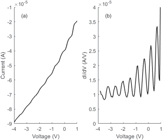
Figure 4. (a) IV curve from QW20 at 100 K under illumination at 660 nm. (b) Differential of the IV curve with respect to voltage.
Download figure:
Standard image High-resolution imagePhotocurrent
The device IV curve at 100 K under monochromatic illumination at 660 nm is shown in figure 4(a). The differential of the IV curve in figure 4(a) with respect to voltage is shown in figure 4(b). The IV curve shows clear steps, which become more apparent upon differentiation. This is consistent with the observations by Khalil et al [14, 16, 17]. It therefore seems likely that there is an asymmetry between the electron and hole QW escape times in this device. If this is the case then the peaks in figure 4(b) indicate the voltages at which the depletion edge coincides with a QW. At these points, increasing the reverse bias voltage causes the QW to become depleted, meaning the majority of the carriers collected by that QW are extracted, rather than recombining.
Whereas the dilute nitride materials investigated by Professor Balkan et al have large conduction band offsets which trap electrons, the dominant effect of Bi incorporation is to raise the valence band edge [30], meaning it is more likely that hole-trapping/collection is the cause of the steps in this device. The carrier escape times will now be estimated based on the assumption that the radiative recombination is dominated by transitions between quantum confined states in the GaAsBi QWs. As dilute bismide materials have been shown to exhibit localised states close to the valence band edge [24, 31–33], it is possible that the holes will need to overcome a larger potential barrier to escape. This would have the impact of increasing the electron and hole escape time disparity that will be found in the next section.
Carrier escape time calculations
The 1D time-independent Schrödinger equation was used with a Hamiltonian given in the effective mass approximation, along with the previously measured QW width (4.8 nm [20]) and estimated ground state transition energy (see figure 2), to find the energy levels of the carrier bound states in QW20.
When applying boundary conditions to the calculation of carrier wavefunctions at a heterojunction, there is no clear consensus in literature as to whether  or
or  should be made to be continuous. In this work, the continuous
  boundary condition (the so called BenDaniel–Duke boundary condition [34]) was employed to ensure conservation of particle flux, given that the effective masses are distinct in each material [35]. The effective masses used in this work for GaAsBi were 0.063 me, 0.45 me, and 0.23 me for electrons, heavy holes, and light holes respectively [35]; the effective masses for GaAs were taken to be 0.063 me, 0.51 me, and 0.082 me for electrons, heavy holes and light holes respectively.
The Bi content in the wells was set at 5.0%, to give a ground state transition energy that agreed with the first Gaussian peak energy measured at room temperature. The valence and conduction band offsets were calculated to be 223 and 117 meV respectively, using the model in [27]. The bound state energies at RT are plotted in figure 5(a), against the band profile of the QW.
From figure 5(a), there is one electron bound state, three heavy hole bound states, and two light hole bound states. The bound state energy is smaller for lh1 than for hh1, due to the greatly increased light hole effective mass in GaAsBi [35]. The calculated energy splitting between e1 and the hole states is shown in table 1.
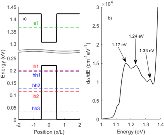
Figure 5. (a) Band profile of a GaAsBi/GaAs quantum well containing 5.0% bismuth at 300 K (black). Also plotted are the energy levels of the bound states inside the well (dotted lines). The wells are assumed to be square, to have a type-I band alignment with GaAs, and to not interact with adjacent wells because of the relatively thick 20 nm barriers. (b) Derivative of the absorption coefficient α, with respect to the photon energy E.
Download figure:
Standard image High-resolution imageTable 1. Calculated transition energies from 1D time-independent Schrödinger equation.
| Transition | Calculated energy (eV) |
|---|---|
| lh1 → e1 | 1.167 |
| hh1 → e1 | 1.171 |
| hh2 → e1 | 1.240 |
| lh2 → e1 | 1.253 |
| hh3 → e1 | 1.336 |
The derivative of the absorption coefficient in this device with respect to the photon energy, dα/dE, is shown in figure 5(b) for comparison. There are several peaks in dα/dE due to higher order transitions in the QW. The positions of these peaks are in excellent agreement with the calculated transition energies shown in table 1, confirming that the band alignment between the wells and barriers in this device is type 1. The small feature at around 1.12 eV is an artefact of the measurement, caused by the changing of the internal filter in the monochromator beam path.
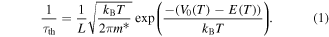
The band offset (V0) and the energy of a bound state (E) dictate the mean time it takes for a carrier to thermally escape the QW (τth) at a given temperature, as shown in equation (1) [36]. Here L is the well width, m* is the carrier effective mass, and kB is the Boltzmann constant
Here, we note that the band offsets are not necessarily constant with temperature. Under the assumption that any reduction in the temperature dependence of the band gap occurs in the valence band, it is found that the valence band offset increases roughly linearly from 223 meV at 300 K, to 237 meV at 100 K. This was determined by varying the valence band offset to produce the observed temperature dependence of the ground state transition energy, and has a minor effect on the calculated thermal escape times. The bound state energies and carrier thermal escape times were calculated as functions of temperature, see figure 6.

Figure 6. Thermal escape times for carriers in bound states inside the well, as a function of temperature.
Download figure:
Standard image High-resolution image
The thermal escape time of electrons at room temperature is extremely short (0.4 ps), compared to holes in the hh1 and lh1 states (250 ps and 200 ps respectively). This is due to the relatively small conduction band offset in GaAsBi.
At 100 K, the electron thermal escape time is still very short (50 ps), but the thermal escape time for holes is increased greatly (7.9 ms and 8.7 ms for hh1 and lh1 respectively). The slow escape of holes from the QWs leads to an accumulation of positive charge in steady state.
This positive charge screens the electric field within the device and reduces its quantum efficiency. The application of a reverse bias causes stepped increases in quantum efficiency as the depletion region expands to encompass individual QWs.
The positive charging of the QWs due to the escaping electrons will alter the potential profile of the QWs [18, 19]. This effect has not been considered here, but would reduce the potential barrier seen by the holes in the QW and reduce their escape time. A more accurate model of the escape times would include this term, but it would only act to reduce the disparity between the electron and hole escape rates following a net charging of the i-region.
The carrier trapping observed in this work has implications for photovoltaic performance. Alemu et al [18] showed that the local potential modification caused by the preferential escape of one kind of carrier (in their case light holes) from a QW, could modify the escape times of the other carriers from that QW. They found that a large overall escape asymmetry reduced the open circuit voltage of their devices through in-built electric field screening. On the other hand, Alonso-Alvarez et al [19] suggested that the enhanced carrier lifetime caused by asymmetric carrier escape could be beneficial to PV performance, along with the ability to use the i-region charging to effectively compensate any unintentional i-region doping.
In order for dilute bismides to fulfil their potential for high efficiency photovoltaics [11, 37], the carrier escape sequence must be carefully considered. Future devices could potentially alloy GaAsBi with N [38] or In, permitting control over the band offset ratio. Alternatively, the device design could be altered to reduce the potential barrier that the holes must overcome to escape the QWs, as suggested by Wen et al [39].
Conclusion
The IV characteristic of a GaAsBi/GaAs, 20 period MQW diode at 100 K is shown to exhibit a 'step-like' appearance under long wavelength illumination. It is postulated that this effect is caused by a similar mechanism to that observed in a study of an InGaAsN MQW device by researchers at the University of Essex. In this case the large valence band offsets in the GaAsBi/GaAs MQW cause a trapping of holes resulting in a screening of the in-built electric field and a reduction of the depletion width. This explanation is supported by calculations that show electron and hole QW escape times that differ by several orders of magnitude. This work indicates that new approaches may be required for future GaAsBi based MQW devices; this may involve alloying with N or In to reduce the necessary valence band offset, or careful device design to aid carrier extraction.
Acknowledgments
The work of R D Richards was supported by the Royal Academy of Engineering under the Research Fellowships scheme. The work of T B O Rockett was supported by the EPSRC (UK). The work of M R M Nawawi was supported by Universiti Teknikal Malaysia Melaka. A. Mellor was supported by the European Commission through Marie Sklodowska Curie International Fellowship, Grant No. DLV-657359
The authors would like to thank Dr B Royall, Dr C A Broderick, and Dr N J Ekins-Daukes for useful discussions.