
Abstract
Using continuous-wave optical pumping of a spin-VCSEL at room temperature, we find high spin amplification of the pump close to threshold within the communications wavelength window, here at 1300 nm. This facilitates a strong switch from left to right circularly polarised light emission, which has potential applications in polarisation encoding for data communications. We use a simple spin flip model to fit the experimental results and discuss the VCSEL parameters that affect this amplification.
Export citation and abstract BibTeX RIS

Original content from this work may be used under the terms of the Creative Commons Attribution 3.0 licence. Any further distribution of this work must maintain attribution to the author(s) and the title of the work, journal citation and DOI.
1. Introduction
Spintronics—the exploitation of the spin degree of freedom in semiconductors—brings a new functionality to optoelectronic devices. Spintronic lasers can be realised as vertical cavity surface emitting lasers (VCSELs), where the vertical geometry and conservation of angular momentum allows the transfer of electron spin to optical ellipticity. Attributes of spin-VCSELs such as threshold reduction [1–3], polarisation control [4–10] and spin amplification [4–6, 9] have been demonstrated. In addition to these static properties, the fast spin-dynamics of these lasers have been investigated [9, 11–19], and promise enhanced performance for applications such as high data rate communications. However, the static properties of spin VCSELs still bear considerable study to improve the general understanding of their behaviour, as such knowledge will aid device engineering for a range of applications.
In this work, strong increases in the ratio of output (VCSEL) to input (pump) polarisation ellipticity are demonstrated, i.e. amplification of spin information, for a range of pumping rates near threshold. This is seen as a rapid transition between left and right-circular VCSEL polarisation (LCP, RCP) for small changes in pump ellipticity. Similar strong switching has been reported before in [8, 9]. In the former case, for an external cavity (VECSEL) emitting at 1500 nm, only relatively low resultant ellipticities of the VCSEL output were achieved, even for completely circular input (pump) polarisation. In the latter case, pulsed optical pumping was used in a GaAs VCSEL emitting at 880 nm, which is somewhat less attractive for potential practical applications. Here we demonstrate that strong switching can be achieved between highly elliptical polarisations for only small changes in pump ellipticity, using CW optical pumping at room temperature in a 1300 nm VCSEL. In addition to measuring this behaviour experimentally, we compare to theory using a simple spin flip model (SFM) [20, 21]. This offers insight into how parameters such as the VCSEL birefringence and dichroism may affect this behaviour.
2. Experimental set up
We use a dilute nitride quantum well (QW) 1300 nm VCSEL wafer grown at Tampere University of Technology, Finland. Our VCSEL design consists of 20.5 pairs of AlAs/AlGaAs bottom mirror layers, 5 groups of GaInNAs QWs of 3 layers each, arranged at the antinodes of the field profile, and has 16 mirror pairs on the top. The top and bottom mirror reflectivities were calculated as 99.2% and 99.8% respectively. The device is described more fully in [7].
The experimental setup is illustrated in figure 1. The wafer was pumped at 980 nm using a cleave-ended Corning HI1060© fibre, and this was expected to produce a highly uniform pump spot. The fibre was held in a manual and piezo-controlled stage. The VCSEL emission from the top of the cavity was coupled directly into the fibre and passed to the various instruments for analysis, whilst the free space output from the bottom of the cavity was collimated and sent to a free space polarimeter (FSP). Interchangeable filters were used so that only the 1300 nm VCSEL or the 980 nm pump light was transmitted to the FSP for the polarisation state to be recorded. The VCSEL spectra were recorded on an optical spectrum analyser. An in-line fibre polarimeter (ILP) was also used, with the fibre connections and additional components in the path ensuring spectral transmission of either only the pump or the VCSEL. The change in the Stokes vectors in the fibre path VCSEL or pump to ILP was measured and the appropriate corrections were applied to extract the final polarisation state, following a procedure described previously [7, 22, 23]. Using the two polarimeters therefore enabled the pump and VCSEL polarisations to be recorded simultaneously and independently [7, 22, 23].

Figure 1. Experimental set up and fibre alignment. (a) Fibre and free space connections. Key to components not described in text: Iso: isolator; PC: polarisation controller; circ.: circulator. (b) Wafer pinned to mount with fibre alignment. The fibre is butted onto the wafer during experiments.
Download figure:
Standard image High-resolution imageThe laser wafer is unprocessed and contains no lateral waveguiding. We found that with a 6 μm diameter spot from the single mode fibre, a high optical pump power at 980 nm was required to achieve threshold, typically between 140 and 200 mW. The factors which determine the lasing mode arise from the spatial carrier density distribution generated by the pump spot, and include a combination of gain guiding, strong index antiguiding via the alpha factor, and thermal lensing. The lack of built in index guiding compared to a typical electrically pumped VCSEL would also be an important factor. This, together with a low level of overall pump absorption leads to high pump power required for threshold; a similar value was reported in [4] for optical pumping of a spin-VCSEL. To mitigate excessive heating at high pump power the sample was maintained at 15°–17° using a Peltier device.
3. Experimental and numerical results
3.1. Experiment
Using the experimental set up described in section 1, the pump power and the fibre position were adjusted to achieve lasing, the latter using the mechanical and piezo adjustments on the stage. The fibre position was carefully adjusted to provide the best compromise of stability via anchoring on the wafer surface, a low threshold, and good coupling of 1300 nm laser light back into the fibre. Firstly, the LI curve was generated to accurately determine the laser threshold. The VCSEL power for the LI curve was integrated from the lasing spectra on the OSA, with a bandwidth of 2 nm. As this is much less than the gain bandwidth, the amount of spontaneous emission included was small, thus the lasing threshold was clear from the rapid increase in power, being at 740 ± 1 mA. The spectra and LI curve are shown in figures 2(a), (b) where the pump currents I used in the polarisation measurements of 760, 800, 850 and 900 mA are shown by the red vertical lines. The pump power range is 169 mW (760 mA) to 201 mW (900 mA). These correspond to pumping rates of 1.03, 1.08, 1.15 and 1.22 × Pth using equation (1). This is based on the pump current/power relation, which was determined as linear in this range

Figures 2(c), (d) shows the measured variation of the VCSEL polarisation with that of the pump at the four pumping rates mentioned above; each response was measured twice. The polarisation responses show that for pumping rates close to threshold (red and black curves), the degree of circular polarisation, i.e. the Stokes S3 parameter, switches sharply from near LCP (S3 = −1) to near RCP (S3 = +1) and back for small changes in pump polarisation around pump S3 of zero. As the pumping rate is increased (blue, green curves), the characteristic softens to a more gradual change. Although the generatrend of softening RCP, LCP transition with increased pumping applies, it is seen that the transition is sharpest at 1.08 × Pth (red curve). Here the VCSEL S3 approaches a maximum value at pump S3 of around ±0.15, then falls back slightly. In fact the results at 1.03. and 1.15 × Pth also demonstrate this behaviour, although the effect is subtle in those cases by comparison. Further from pump linearity, i.e. S3 > 0.25, the VCSEL S3 values show a consistently reducing trend with increasing pump rate, which is the expected result.
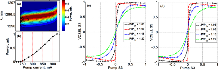
Figure 2. LI curve defining pump rates, and variation of VCSEL S3 with pump S3 for four of these pumping rates. (a) Spectra (b) LI curve (power from spectra) (c) first set of results (d) second set of results. The dashed connecting lines between polarisation points in (c) and (d) were fitted using a cubic spline.
Download figure:
Standard image High-resolution imageThe absolute VCSEL S3 valuesear pump S3 = 0 in figures 2(c), (d) is seen to be considerably greater than the absolute pump S3 values. This means there is amplification of the spin i.e.  The cause of this amplification and sharp switching is the proximity to threshold of the RCP, LCP modes at low pump rates: the LCP or RCP lasing output increases very rapidly as threshold is achieved, whilst the other mode is suppressed. However higher pumping rates soften this change. This rapid lasing transition is achieved despite the spin-up, spin-down electron populations being very similar, even for circular pumping. This is due to the rapid balancing of up, down populations from the spin relaxation time being much shorter (∼1/100) than the electron recombination lifetime. The spin amplification for the polarisation responses in figures 2(c), (d) were calculated, and these are shown in figure 3. The maximum amplification values (which occur closest to pump linearity) increase from approximately 2.8 at the highest pump rate to over 20 at t lowest pump rate (closest to threshold). However away from this trend, the particularly sharp LCP, RCP transition at 1.08 × Pth. discussed above produces very strong amplification, with calculated values there of over 1000 (figure 3(b)). This spin amplification is potentially very useful in applications. It should be noted that to determine accurately the peak amplification very close to pump S3 = 0 requires the pump S3 to be measured very accurately, as any systematic error in the pump S3 will strongly distort the calculated amplification. Here, any systematic errors identified in the measured pump S3 were eliminated prior calculation of the spin amplification, by a correction in the pump S3 of typically 0.02.

Figure 3. Calculated spin amplification for the first set (in black) and second set (in green) of experimental results (a) 1.03 × Pth, (b) 1.08 × Pth, (c) 1.15 × Pth, (d) 1.22 × Pth. The calculated spin amplification in (b) for the first experimental result reaches extremely high levels, which are of the range of both the main and inset graph.
Download figure:
Standard image High-resolution imageFor a practical device there will be growth variations in the different mirror, passive and active material layers across the wafer, and this will affect device parameters such as birefringence, dichroism and photon lifetime. These parameters are defined in appendix A1 and are discussed further in section 3.2. Furthermore there may be varying strain from the anchoring of the fibre on the wafer, which may suppress or excite different lateral modes of the device, noting that there is no lateral mode confinement in the sample and these modes have been shown to have associated polarisation behaviour [24, 25]. Because our wafer is optically pumped with a fibre, imaging of the lateral modes was not possible (as opposed to electrical pumping, where a camera can be positioned to image the output relatively easily e.g. [26]). With these influences in mind, to ascertain that the sharp LCP-RCP transitions and corresponding amplification found above were repeatable, the experiment was repeated in different areas of the wafer, and figure 4 presents typical results. In figure 4(a) for pumping rates from 1.04 to 1.13 × Pth, the polarisation responses show the expected softening of the LCP-RCP transition with increasing pump rate. In figure 4(b) for the pump rate increasing from 1.13 to 1.32 × Pth, the softening is seen to reverse however, with the transition becoming sharpest at the highest pump rate. Comparing the resultant spin amplification rates in figure 4(c), the lowest and highest pumping rates of 1.04 and 1.32 × Pth therefore show the highest amplification, of approximately 8 (black and grey lines there, note the different colour keys in these figures). Here there is no anomalous increase then decrease in  with increasing
  that was seen at 1.08 × Pth see figures 2(c), (d). In other measurements, we have consistently observed that effect, and have also observed a more consistent softening of the LCP-RCP transition with increasing pump rate. These results demonstrate that good amplification and a sharp LCP-RCP transition can still be achieved consistently across a large sample (5 × 5 mm), despite the different influences on results. The maximum spin amplification of 8 in figure 4, and above 20 in figure 3 compare to a spin amplification corresponding to around 3.8 reported in [5]. It is noted that very high amplification vues are in evidence in [9], achieved with pulsed optical pumping in an 880 nm device.
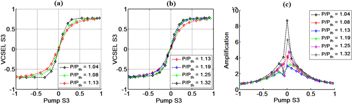
Figure 4. Additional polarisation responses and amplification rates found at a different location on the wafer than figures 2, 3 (a) lower and (b) higher pumping rates (c) corresponding amplification rates for these polarisation responses. Note the different colour keys for these figures.
Download figure:
Standard image High-resolution image3.2. Comparison of experiment and SFM
A comprehensive model of the simple experimental measurements which have been taken using a small polarised photopumped spot (typically 6–10 μm in diameter) to excite a planar wafer is a complex task because there are a number of competing and interdependent effects. For example, to determine the electromagnetic field behaviour in such a weakly guided system, account must be taken of the spatial distribution of the pump and the resultant distribution of carriers. This feeds into the field solutions both via the gain and refractive index [27] using the SFM (to include polarisation), in a similar way to the approach in the extended SFM that has been used for conventional electrically-pumped VCSELs [24], but now including the polarisation of the pump. It would also be necessary to include thermal lensing effects in such a model to account for the spatial temperature distribution [25]. To do all this accurately in a single self-consistent model requires knowledge of many key parameters, many of which are not well established. Thus in order to gain some insight into the experimental behaviour we make the simplifying assumption that the responses can be modelled using the SFM alone. While clearly limited in applicability this does provide an accessible approach to assessing the main features of the experimental results.
To compare the modelled results with those from experiment, the VCSEL S3 response to pump state was generated using the SFM (see appendix A1 for definition of equations and terms). It has been shown [28] that the polarisation response of the SFM is dependent on the ratio of a number of key parameters, most notably the ratios of birefringence and field decay rates, γp/κ, and electron spin relaxation and recombination rates, γs/γ. Therefore variation of these two ratios whilst maintaining reasonable individual parameter values in the SFM, and comparing modelled and experiment results is a useful method to initially determine parameters. For a ratio γs/γ of 64, a ratio γp/κ of 0.00125 gave reasonable agreement experiment (figures 2, 3 results) to model, with further optimisation producing a γp/κ value of 0.0014. The γs/γ ratio of 64 is in good agreement with values of these two parameters reported in the literature see appendix A2. Calculation of the field decay rate κ for a device is again relatively straightforward and accurate, and a value of 68.5 ns−1 is derived in appendix A2. The remaining parameter of the linear birefringence γp (and the linear dichroism, γa) is more difficult to predict and must generally be measured for a particular VCSEL. This has been done in e.g. [29, 30], but depends on the lasing linewidth being relatively small (here they are around 0.4 nm or 40 GHz see figure 2(a)) and use of a high resolution spectrometer, which was not available here. Therefore the birefringence was simply derived from the calculated κ at the optimised ratio γp/κ of 0.000 14, being 0.1 ns−1 for κ of 68.5 ns−1. This birefringence is low for a VCSEL, but is thought to be reasonable for the residual value found in the planar wafer. A small, positive dichroism value γa of +0.1 ns−1 was initially estimated as part of the optimisation process. This fits reasonably with reported values [29, 30]. A somewhat higher dichroism of 0.5 ns−1 was also investigated, and this is detailed below.
Using the SFM parameters described above, the VCSEL S3 values were generated from the SFM for the four pumping rates from figures 2, 3, γa of +0.1 ns−1 and the varying pump ellipticity. The SFM pumping rates η are derived from the scaled experimental pumping rates, as described in appendix A2. The SFM results are compared with the experimental S3 values and spin amplification rates (as per figures 2(c), (d) and 3) in figure 5. The SFM S3 values (in red) in figures 5(a), (c), (e), (g) follow the experimental results reasonably well, particularly near pump S3 = 0 where the spin amplifying properties are defined. The corresponding spin amplification rates in figures 5(b), (d), (f), (h) are also reasonably close in experiment and model. For the chosen dichroism in the SFM of 0.1 ns−1, the amplification is somewhat higher at lower pumping rate in the experiment, and lower at higher pumping rates.
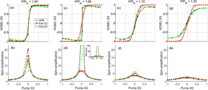
Figure 5. Pump and VCSEL polarisation S3 responses and spin amplification; (a), (c), (e), (g) S3 responses (b), (d), (f), (h) spin amplification. The legend indicates the SFM, first ('Exp (1)') and second ('Exp (2)') set of experimental results. The calculated spin amplification in (d) for the first experimental result reaches extremely high levels, which are off the range of both the main and inset graph. No interpolation between points was performed here.
Download figure:
Standard image High-resolution imageA further comparison experiment to model is shown in figure 6 describing the change in VCSEL ellipticity for a finite pump ellipticity of +0.31. This value of ellipticity was chosen here to reveal the spin amplification properties of the VCSEL. The experimental results were collected for the same wafer area and fibre alignment as per figures 2, 3, 5 results. The VCSEL S3 values in figure 6 are seen to match those values well (at the respective pump rates and pump ellipticity) and this again reveals the spin amplification, as the VCSEL ellipticity remains above 90% from 1.02 to 1.12 × Pth, for the pump ellipticity of only 0.31. The experimental pumping rates have been scaled up to the equivalent SFM pumping rates η here. The SFM results are for γa of 0.1 ns−1, and additionally a higher γa of 0.5 ns−1, which was mentioned above. The lower value of dichroism is seen to produce a better fit at the lower pumping rates, and the higher dichroism is seen to produce a better fit at the higher pumping rates. These modelled results indicate reasonable boundaries of the suitable dichroism value to model these results in the SFM. As the dichroism could not be measured and verified in this case, the divergence between experiment and model might lie in changes such as increases to birefringence (which will also soften the LCP-RCP transition), dichroism, or indeed excitation of different lateral modes of the wafer. A final comment on the SFM parameter values is that the tuning of 0.18 nm over the pumping range seen in figure 2(a) indicates a change in temperature of the overall VCSEL of around 1.6° using a cavity shift of 0.11 nm per degree [31]. Therefore it is not reasonable here to ascribe the divergence in modelled to experiment results to a reduction in spin lifetime from the temperature-dependent D'Yakanov–Perel effect [32], which might otherwise be posited as a cause.

Figure 6. VCSEL ellipticity in the experiment, and in the model for two values of dichroism and fixed pump ellipticity. The sharp change in VCSEL S3 below threshold in the experiment indicates modal changes, with an associated polarisation change.
Download figure:
Standard image High-resolution image3.3. Approximate solution of the steady-state SFM
In order to explore further the spin amplification and its dependence on parameters, an approximate solution of the SFM equations has been developed. The approach follows that in [33] and the only requirements on the range of parameter values are  and
and  , both which are satisfied by the values used in fitting the experimental results here. Details are provided in [34], giving the derivation of a useful algebraic relation between the normalised pumping rate η, the ellipticity of the pump P (
 ) and the ellipticity of the output ε (
 ). This relation gives excellent agreement with results from numerical solution of the full SFM for plots of P versus ε over the full range from −1 to +1, similar to those in figures 4 and 5. We give here the limiting expression that is valid for the spin amplification at small ellipticities:

The simple form of equation (2) makes it easy to see the dependence of maximum spin amplification (ε/P) on the SFM parameters. Figure 7 gives an example of its application in demonstrating the dependence on total pump rate and dichroism.

Figure 7. Calculated spin amplification ε/P versus pump/threshold for different values of dichroism rate.
Download figure:
Standard image High-resolution image4. Discussion
These results show that the sharp LCP-RCP transition i.e. spin amplification found experimentally, can also be predicted theoretically using a simple SFM. Using this there are some differences between the experiment and modelled results and to attempt to fully account for these a more complex model is required. In addition, multiple lateral modes can affect the polarisation response, so determining the modal properties experimentally, and modelling their effects [25] should also be considered. Nevertheless with the SFM alone we see some indication of the sensitivity for high spin amplification to the parameters γa and γp, as discussed in [8, 10–19], and it is clear from the SFM (see equation (2)) that minimisation of γa and γp is essential for high spin amplification. Practically this might be achieved by balancing residual strain in the device by methods such as temperature control, patterning or application of mechanical stress. Additional gains may be had, for example, by tailoring of the position of the LP modes with respect to the wavelength of the gain peak to minimise γa, and utilising the change in the alpha parameter with lasing wavelength (see appendix A.1).
5. Conclusions and future work
We have demonstrated spin amplification and switching of the Stokes S3 parameter in a 1300 nm spin-VCSEL with CW optical pumping at room temperature, and shown high values of spin amplification near to threshold. We compared these experimental results with those predicted by a simple SFM of spin amplification which contains the key parameters of birefringence, dichroism, spin relaxation rate, carrier recombination rate, field decay rate, linewidth enhancement factor and pumping rate. A pumping rate—dependent polarisation response has been identified which increases the amplification and switching strength, and which is not found in the SFM.
One explanation for the differences identified between the experimental and modelled results may be due to changes in parameters from effects such as heating and excitation of different lateral modes. Furthermore, this work has revealed the importance in identification of the birefringence and dichroism parameters, as these are critical to the spin VCSEL polarisation response. We believe a more complex model taking account of a number of spatial effects including the lateral waveguide properties and other parameters, simultaneously with the polarisation responses, is required to fully understand the experimental behaviour.
Acknowledgments
This work has been funded by the UK EPSRC (Grant Nos. EP/G012458/1, EP/M024237/1, EP/M024156/1).
Appendix.: The SFM and derivation of parameters
A.1. Spin flip model
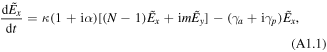
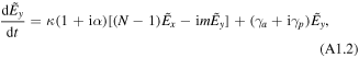
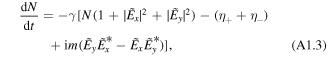
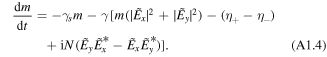
The SFM in terms of the complex linearly polarised fields  is written as in equations (A1.1)–(A1.4) [21], with N as the normalised total spin up and down electron density
  m the difference in normalised electron densities
 the spin up, down pumping rates, γ the electron recombination lifetime, γs the electron spin lifetime, κ the field decay rate, α the linewidth enhancement factor, γa the linear dichroism and γp the linear birefringence
A.2. Derivation of the SFM parameters
The threshold modal gain for a laser is derived as per equation (A1.5), with  the threshold gain,
  the material losses,
  the losses from the mirror transmission out of the cavity,
  the effective cavity length and
  the bottom and top mirror reflectivities

The material losses  for GaInNAs have been reported as 700 m−1 [35, 36], and the mirror reflectivities
  for this device are 99.2% and 99.8% [7]. The effective cavity length
  is the 3-λ cavity length [7] of 3.9 μm. With the mirror penetration depths calculated as 0.61 μm [37], the cavity length
  is then 5.12, giving the threshold gain
  as 1644 m−1.
The corresponding field decay rate κ is half the intensity decay rate, as per (A1.6), with c the vacuum speed of light and ng the group index. Using a group index ng value of 3.6 from [38] then gives κ as 68.5 ns−1

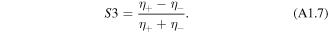
The Stokes S3 parameter of the pump is defined in terms of the pump rates  as per (A1.7). From this, the pump rates
  can easily be derived in terms of the total pump rate
  and the pump S3 polarisation
The total pump rate η is scaled from the experimental pump rate above threshold  as the ratio of transparency to threshold gain as per (A1.8), giving a 43% over-unity scaling of the pump rate

The electron recombination lifetime γ was taken as 1 ns−1 [7]. The electron spin relaxation rate γj has been measured as 33 ns−1 in this material, when rapidly thermally-annealed [39]. As the mirror growing process is expected to anneal the active region [40], we have taken this as a reasonable value for our VCSEL. Using the relation between the measured spin relaxation rate γj, the recombination rate γ and the SFM spin relaxation rate  gives a value for γs of 67 ns−1, close to the value of 64 ns−1 that was selected in section 3.2.
Finally, the (Henry) α parameter in GaInNAs quantum well lasers has been calculated in [31], and has also been measured experimentally in [41]. These show close agreement, with a value close to 2.0 at 1300 nm. It should be noted that both show a slightly reduced value of around 1.8 at 1290 nm, and significantly larger values at 1310 nm. As the value is sensitive to the exact material composition [31], 2.0 was chosen as a suitable value for this work.


