

Abstract
This is an update of a previous review (Naumis et al 2017 Rep. Prog. Phys.80 096501). Experimental and theoretical advances for straining graphene and other metallic, insulating, ferroelectric, ferroelastic, ferromagnetic and multiferroic 2D materials were considered. We surveyed (i) methods to induce valley and sublattice polarisation (P) in graphene, (ii) time-dependent strain and its impact on graphene's electronic properties, (iii) the role of local and global strain on superconductivity and other highly correlated and/or topological phases of graphene, (iv) inducing polarisation P on hexagonal boron nitride monolayers via strain, (v) modifying the optoelectronic properties of transition metal dichalcogenide monolayers through strain, (vi) ferroic 2D materials with intrinsic elastic (σ), electric (P) and magnetic (M) polarisation under strain, as well as incipient 2D multiferroics and (vii) moiré bilayers exhibiting flat electronic bands and exotic quantum phase diagrams, and other bilayer or few-layer systems exhibiting ferroic orders tunable by rotations and shear strain. The update features the experimental realisations of a tunable two-dimensional Quantum Spin Hall effect in germanene, of elemental 2D ferroelectric bismuth, and 2D multiferroic NiI2. The document was structured for a discussion of effects taking place in monolayers first, followed by discussions concerning bilayers and few-layers, and it represents an up-to-date overview of exciting and newest developments on the fast-paced field of 2D materials.
Export citation and abstract BibTeX RIS

Original content from this work may be used under the terms of the Creative Commons Attribution 3.0 license. Any further distribution of this work must maintain attribution to the author(s) and the title of the work, journal citation and DOI.
Recommended by Dr Nandini Trivedi
1. Motivation and Update's structure
One Review of strain and the electronic and optical properties of graphene and other 2D materials appeared six years ago [1]. Exciting advances since then include (1) strain on lateral superlattices; (2) non-linear Hall effects, Berry dipoles, and exotic quantum phase diagrams due to strain in graphene; (3) the experimental verification of piezoelectricity in hexagonal boron nitride (hBN) monolayers; (4) the creation of strain by a sudden thermal quenching during 2D material growth and the effects of strain on the optical properties of transition metal dichalcogenide (TMDC) monolayers; (5) the role of strain on 2D phase transitions in 2D ferroelectrics and ferromagnets; (6) twisted (moiré) 2D materials exhibiting flat electronic bands; (7) the role of local and global (and even time-dependent) strain on superconductivity and topological phases of twisted few-layer graphene; (8) magnetoelectric couplings on 2D magnetic bilayers; among others. Previous list of topics contains strained monolayers (topics 1 through 5) and few layers (topics 6 through 8) under strain. Strain is an integral part of the field of 2D materials, and recently synthesised 2D materials such as (Quantum Spin Hall) germanene, (elemental ferroelectric) bismuth monolayers, and (magnetoelectric multiferroic) NiI2 monolayers–all adding functionalities and additional 2D material platforms–are featured here as well.
The Update is written to reflect that order: section 2 lists experimental techniques to strain 2D materials, section 3 contains a discussion of strained graphene, piezoelectric hBN monolayers, strained TMDC monolayers, ferroelectric and magnetic 2D materials under strain, and section 4 is devoted to strained bilayers and multilayers (including moirés, ferroelectric and antiferroelectric bilayers, as well as engineered multiferroic bilayers). Recently synthesised 2D materials appear within those sections. Conclusions are presented in section 5.
2. Experimentally available methods to strain 2D materials
The most common strategy for straining 2D materials involves placing them into flexible polymer substrates, which are bent or stretched afterwards [1]. Nevertheless, adhesion is usually weak, preventing strain from being fully transferred [2]. This limitation calls for novel techniques to produce strain, and the following processes are being pursued to that end:
- (i)Propagating potential traps induced by surface acoustic waves (SAWs) in h-BN encapsulated bilayer WSe2 [3].
- (ii)Time-dependent piezoelectric substrates [4].
- (iii)Reversible ion intercalation in multilayers [5].
- (iv)
- (v)
- (vi)
- (vii)
- (viii)
- (ix)
- (x)Thermally-induced strain on 2D materials undergoing 2D phase transformations [26].
- (xi)
- (xii)
- (xiii)
Prior to undertaking the main task of this Update, it may be necessary to reassess the physical meaning of mechanical strain and to disclose the definition followed here. Before the atomistic hypothesis was born, strain was a measure of mechanical stress and of the elasticity of bulk materials at finite temperature, without concern for their microstructure. In this sense, strain is an out-of-equilibrium mechanical modification of a material. Examples of this definition include topics (i) through (vi) in the list above.
But, sometimes strain is also thought of as a modification of a 'pristine' (crystalline) zero-temperature lattice. In other words, though a lattice may be in mechanical and thermal equilibrium (and hence unstrained in the strictest sense of the word), its lattice parameters or atomic positions may have changed with respect to those in the pristine scenario. Examples of that definition of (permanent–or quasi-permanent in case a nano-bubble were to explode, or temperature changed through a 2D phase transition) strain include processes (vii) through (xiii).
Both uses of the word strain are employed by the community, and it is important to make the point that those definitions are not identical.
The effect of strain on materials' properties is studied in what follows.
3. Strained monolayers
Strain affects the electro-optical properties of 2D materials due to the stretching, bending and torsion of chemical bonds. Stretching has the largest effect because it alters electronic hopping between atoms the most [39].
3.1. Updates on graphene strain engineering
The most common theoretical approaches for graphene's strain engineering are tight-binding (TB) methods, the low energy approximation in a continuum or within a discrete lattice, and density-functional theory (DFT) calculations [1].
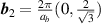
Aiming for continuity of the theoretical descriptions, the notation and definitions used in [1] will be maintained. For example, graphene's zero-temperature lattice vectors are still given by:
where a = 1.42 Å is the distance between carbon atoms. Standard notation for atomic displacements induced by strain is kept unchanged as well, so that atomic positions under deformation are given by this field:

with in-plane displacements given by  and out-of-plane displacements denoted by
  , where
  is a 2D position vector. The strain tensor
  (with components
  ) is related to the deformation field as follows:

3.1.1. Correcting second- and third-nearest neighbour interactions on empirical tight-binding Hamiltonians.
There are quantitative discrepancies between calculated electronic properties using DFT and TB methods without ab initio input. The π-electron TB Hamiltonian for strained graphene is given by [1]:
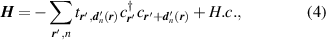
where  runs over all sites of the deformed honeycomb lattice and the hopping integral
  varies due to changing interatomic distances. The operators
  and
and  create an electron at
  and annihilate another at
  . Vectors
  include multiple nearest neighbours and thus update equation (51) in [1], which included first-nearest neighbours only.
Considering up to third-nearest neighbours, the disagreement between DFT and a first-nearest neighbour TB Hamiltonian without ab initio corrections was tracked down to an angular dependence of the TB hopping parameters for second- and third-nearest-neighbours [40]. Figure 1 shows that the TB parameters up to third-nearest neighbours are modified depending on the angle of the tensile deformation. The radius of the blue and red circles in figure 1 is the deviation from the TB hopping parameter. Large corrections of the TB Hamiltonian are observed in second- and third-nearest neighbour interactions [40]; those corrections must be added to the Hamiltonian set up by Hasegawa et al [41] to describe graphene under tensile strain appropriately.
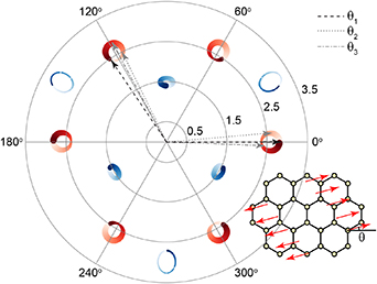
Figure 1. Effect of a uniform (15%) tensile deformations at different angles θ on TB hopping parameters. Three sets of lattice vectors for different values of θ are shown in the main plot, while the tensile deformation is shown as an inset. The radiuses of the circles indicate the strength of hopping parameters from an atom centred at the origin. The colour red (blue) indicates a positive (negative) hopping parameter. The colour map corresponds to the angle θ, which varied from 0 to π. Second- and third-nearest neighbour interactions require a larger relative correction when compared to first-nearest neighbour interactions. Reprinted with permission from [40]. Copyright (2018) American Chemical Society.
Download figure:
Standard image High-resolution image3.1.2. Corrections of empirical TB Hamiltonians due to spin–orbit coupling.
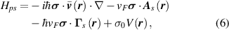
In-plane strain leads to quadratic corrections on spin–orbit coupling [42]. Out of plane deformations, on the other hand, hybridise π-orbitals with  electrons and produce a first-order contribution in the spin-orbit interaction strength [43] with three contributions [42]:

where the labels A1, B2, and Gʹ represent the irreducible representations of the group  , which results from considering a
  supercell with six atoms. The non-primitive cell was employed to avoid dealing with degenerate states at two inequivalent Dirac points [42]. The corrections give rise to a Kane–Mele mass and to a Rashba-like coupling, which is present only when a mirror symmetry is broken [42]. Both coupling effects are weak (in the
  µeV range [42, 44]).
3.1.3. Low-energy effective models: Dirac equation with pseudomagnetic vector potentials.
Low-energy models for non-interacting electrons in graphene with (in-plane) strain and (out-of-plane) flexural deformations [44–48] have found unusual applications, such as the holographic imaging of black holes [49], and other proposals for cosmological models [50].
Other studies relying on low-energy approximations dwell on the optical and electronic properties of graphene [51, 52], on curvature-induced quantum spin-Hall effects in Möbius strips [53], on the topological Hall effect in strained twisted graphene bilayers with enhanced interactions [54], and on the valley-dependent time evolution of coherent electron states in tilted anisotropic Dirac materials [55]. In addition, the optical properties of massive anisotropic tilted Dirac materials [56], valley polarisers and filters [57], the creation of complex magnetic fields [58] or of Landau levels in curved spaces [59], the propagation of pseudo-electromagnetic waves [60], and comparisons between twistronics and straintronics in twisted bilayers of graphene and TMDCs [61] have also appeared in the literature.
The low-energy continuum approximation takes a Dirac equation in two dimensions and a minimal coupling to effective pseudo-electromagnetic fields. The dynamics may include additional contributions caused by  band hybridisation (which is proportional to curvature) and/or by external electromagnetic fields. Nevertheless, this approach only works for small deformations; something most clearly seen when performing the low-energy approximation at each unit cell within the atomistic lattice [62].
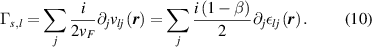
Under large strain, higher-order contributions give rise to sizeable pseudomagnetic fields [63, 64]. Those corrections to the low-energy approximation can be captured through gradient expansions in real space. According to Roberts and Wiseman, corrections with nontrivial frame contribute at the same order as higher covariant derivative terms, and therefore ought to be included [64]. Comparisons against numerical diagonalisation of the empirical TB model seem to be in agreement with their observations [65]. An effective Hamiltonian for non-uniform strain taking the displacement of Dirac points into account looks as follows [66, 67]:
where the position-dependent Fermi velocity tensor  is given by:

with vF
the Fermi velocity ( , where c is the speed of light in vacuum),
  is the Pauli matrix vector and
  labels the valley, and σ0 is the
  identity matrix. In turn, the (deformation) scalar and (pseudomagnetic) vector potentials are given by:

respectively. The dimensionless coefficient β ≈ 2.0–3.0 [68] measures the effect of the deformation on the first-nearest neighbour TB hopping parameter. The coupling g has been renormalised to about 4 eV [69].
The l-component of the corresponding complex vector field  (
( ) is:
) is:
Unlike
A
s
,  is purely imaginary and cannot be interpreted as a gauge field [67, 70]. Experimental signatures of the imaginary field remain elusive, but the term may become important at boundaries. (Boundaries are accounted for in effective-mass approaches of semiconductor heterojunctions by establishing consistency relationships that match atomically-resolved TB states to boundary envelope wave functions [71].) One is to remember that the low-energy approach for strain engineering is a semiclassical approach that mixes real and reciprocal space pictures, which breaks down at boundaries (periodic within neighbouring cells [62] or at edges) unless treated with care.
Indeed, a consistent treatment of boundaries within graphene strain engineering remains lacking. Nevertheless, multiple deformation fields are uniquely determined by boundaries and by sharp strain profiles: as it is the case in semiconductor heterojunctions, effective theories based on envelope wave functions call for supplemental boundary conditions of the form  to retain hermiticity, and for self-adjoint extensions to preserve currents [72–75]. M is a matrix containing microscopic details and symmetries, and ψ is the electron/hole wavefunction at the boundary. Here,
  restores hermiticity. The need for non-Hermitian corrections can also be ascertained by the breakdown of hermiticity as phasors do not add up to zero within individual unit cells under non-homogeneous strain [1, 62].
Debus, Mendoza and Herrmann matched the Hamiltonian in equation (6) and the more common version (denoted with the superindex c here) by means of the following transformations [76]:

where
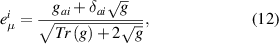
 is the metric tensor associated with strain, δai
is the Kronecker delta,
is the metric tensor associated with strain, δai
is the Kronecker delta,  the square root of the determinant of the metric tensor, and
 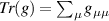 is its trace.
The position-dependent Fermi velocity tensor components obtained from equation (6) were validated on graphene under uniaxial strain εxx
, and used to tune the sensitivity factor of a graphene pressure sensor 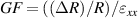 , where R was the resistance and
  the change of R due to strain [77]. Modifications of optical properties under uniaxial strain are detailed elsewhere [78, 79].
On samples with large out-of-plane deformations,  orbital hybridisation leads to corrections [47, 80]:

that must be added to the scalar potential  . Here,
  and α ≈ 9.23 eV.
3.1.4. Electrostatic effects due to substrates.
Substrate deformations can also make the on-site energies vary. Such deformation potential [68] can be treated by decomposing the interaction into a smooth spatial effective potential  [47] and, if the substrate produces a bipartite symmetry breaking, an extra term
  [44], which measures the difference of the electrostatic potential in the A and B sublattices [81].
3.1.5. Cut and folded graphene: sublattice and valley polarisation.
The tearing and subsequent folding of the topmost graphitic layer by an STM tip is depicted in figure 2 [82]. There, the tip approaches graphite right before a step edge, moving across it afterwards (figure 2(a)) [82]. As a result, the tip (i) tears and (ii) folds the uppermost monolayer (figures 2(b)–(d)), creating nonuniform strain at the folded edge. The effects of the resulting effective gauge potential were seen by  measurements taken at locations marked by circles in figures 2(e) and (f) [85]. The splitting of
  peaks (and their weight redistribution) in figure 2(g) are manifestations of localised states on folded graphene [82, 83].
Figure 2. (a) Tip-induced tearing and folding at a step edge. Inset: zoom-in of the folded edge. (b)–(d) Folded graphene on a graphitic surface. Insets are snapshots taken prior to folding. Reprinted with permission from [82]. Copyright (2022) by the American Physical Society. (e), (f) Graphene folding with specific chirality. (g) Localised electronic states at folds. From [83]. Reprinted with permission from AAAS.
Download figure:
Standard image High-resolution imageOne-dimensional electronic bands were created along the longest fold in figure 2(d). There, the axial direction of the fold turned out to be parallel to graphene's armchair direction, and the experimental electronic density [82] was contrasted against a linear chain TB Hamiltonian model, where the strain appears as a modulation of hopping parameters and self-energies [1]. According to the model, the flat bands are topological in nature [86]. Folds also create curvature [87] that pushes π-electrons onto the outer side of the fold [80]. The creation of valley polarisation through folds will be discussed in subsequent pages.
Wu et al [84] (figure 3) revealed a Coulomb blockade, so that their fold acted as a quantum dot. Linear folds as the one in figure 3(a) [84, 88–90] were theoretically studied using continuous models with effective pseudomagnetic fields and TB models. Those folds feature bands originating from a mass term in the Dirac equation [91]. Calculations using the Dirac equation in a continuum and including strain were consistent with measured bound state energies, and predicted valley-polarised currents [84], opening an avenue for graphene folds as straintronic quantum wires [92, 93].
Figure 3. (a) Scanning electron microscope image of a graphene fold (dark line within cyan dashed rectangle). (b) Hall bar device created within the cyan rectangle in (a): graphene is encapsulated with hBN, and Hall bar contacts are made. (c) Device image: side contacts to graphene are labelled G1 and G2, while contacts to the graphene fold (nanowire) are N1 and N2. The red dashed line between blue lines highlights the linearly-shaped strain region. Reprinted with permission from [84]. Copyright (2018) American Chemical Society.
Download figure:
Standard image High-resolution imageTriangular periodic ripples in suspended graphene were found in another work. There, bending was limited to a region few unit cells wide [94]. Triangular ripples are unlike the sinusoidal ripples found in fabrics.
The effects of folds in the electronic structure are modeled with effective pseudomagnetic fields within a continuum picture [95]: one considers a pure deformation perpendicular to graphene's plane, i.e.  . From equations (3) and (9), one gets:

By the definition of uniaxial fold, the deformation field is constant in one direction, say ( ). If periodic, it is expressed by a Fourier expansion:
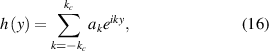
in which the Fourier coefficients obey  (because
  is real), and kc
is a cutoff parameter that can be estimated from experiment [95]. This way,
is real), and kc
is a cutoff parameter that can be estimated from experiment [95]. This way,  has only one non-zero component [95]:
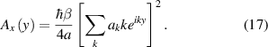
Equation (17) implies that  , so that
  is in the Coulomb gauge. Thus it can be derived from a pseudoscalar magnetic potential:

with  and
and  ij
a 2D Levi-Civita tensor. Expressing
ij
a 2D Levi-Civita tensor. Expressing  as a Fourier series:
with
and
The associated pseudomagnetic field becomes:

 does not produce a pseudomagnetic field, but instead an Aharonov–Bohm effect manifested by a phase change along closed circuits enclosing folds. As
  is derived from
  , zero-modes can always be found for any fold with an arbitrary cross-section (periodic, random, quasi-periodic, etc assuming a large unit cell for the periodic function h(y)), and being topologically protected, their existence is independent of
  . Using equation (6) for E = 0, two wave functions are obtained:
where σz is the Pauli z-matrix. Those topological modes appear as a consequence of the Atiyah-Singer theorem, and correspond to soliton solutions of the Dirac equation with a space-dependent mass [96].
This approach permits exploiting similarities with the integer quantum Hall under a random magnetic field [97]. In such field, the vector potential is given by a gaussian distribution with zero mean and variance  . The average of the coefficients in equation (19) can be expressed as:
From this analogy with real magnetic fields it can be concluded that the wave-function is multifractal [97]. The multifractal localisation can be determined from the participation ratio moments  where L is the sample length [98]:

from where it follows that [97]:
with
Such multifractal conductance fluctuations have been measured in high-mobility mesoscopic graphene devices under external magnetic fields [99]. In addition, edge modes arising in graphene under periodical strain-induced pseudomagnetic fields have been contrasted to those arising under real, periodic magnetic fields [86, 100].
It is now time to address the creation of sublattice charge imbalance, which can be visualised in local density of states (LDOS) calculations and  STM measurements [62, 91, 101–103]. Strain-induced sublattice imbalances create an energy separation of the two pseudospin degrees of freedom due to the pseudomagnetic field Bs
. The creation of charge imbalance can be seen by squaring graphene's Dirac Hamiltonian with the strain-induced pseudo-magnetic field Bs
:
STM measurements [62, 91, 101–103]. Strain-induced sublattice imbalances create an energy separation of the two pseudospin degrees of freedom due to the pseudomagnetic field Bs
. The creation of charge imbalance can be seen by squaring graphene's Dirac Hamiltonian with the strain-induced pseudo-magnetic field Bs
:
where E is the electron's energy, vF
the Fermi velocity,  (
( ) the wave function amplitude on the A (B) sublattice, and
π
the canonical momentum. The term proportional to Bs
appears with opposite signs at each sublattice, shifting their energy in opposite directions and leading to a (Zeeman-like) pseudospin (sublattice) polarisation.
) the wave function amplitude on the A (B) sublattice, and
π
the canonical momentum. The term proportional to Bs
appears with opposite signs at each sublattice, shifting their energy in opposite directions and leading to a (Zeeman-like) pseudospin (sublattice) polarisation.
An STM setup was designed to induce and visualise sublattice imbalance [101]. Similar to [104], the tip lifted graphene from the substrate, creating a gaussian-shaped deformation that moved along with the tip (see figures 4(a) and (b)) and a pseudomagnetic field with 3-fold symmetry (figure 4(c)).  measurements (figures 4(d)–(g)) performed by the same STM tip show increasing sublattice LDOS imbalance with increasing tip current. Analytical expressions for sublattice contrast [103] and molecular dynamic simulations showed good agreement with experiment. Gaussian deformations have been proposed as valley filters [84, 105–110], and as Aharonov–Bohm interferometers [111]. Strain fields similar to those created by gaussian-like deformations were observed in graphene nanobubbles [34].

Figure 4. Sublattice symmetry breaking by gaussian deformations in graphene. (a) Gaussian deformation induced by an STM tip (amplitude H = 1 Å, width b = 5 Å). (b) The deformation (black dashed line) follows the STM tip (whose atomistic structure is depicted by red atoms and a blue apex), leading to the apparent STM image (blue curve) which is lifted with respect to the relaxed one (red curve). Yellow bars represent tunnelling currents. (c) Pseudomagnetic field pattern of the gaussian deformation of panel (a). The brightness corresponds to the LDOS calculated from a first nearest neighbour TB Hamiltonian. Insets (white squares) are areas of maximum Bs . (d)–(g) Constant-current STM images of the same graphene area. Hexagons and the two sublattices were overlaid. The LDOS is higher in the sublattice corresponding to the red dots at higher currents. Reprinted with permission from [101]. Copyright (2017) American Chemical Society.
Download figure:
Standard image High-resolution imageProducing valley-polarised states is the aim of valleytronics [113, 114]. However, there are important differences between graphene's valley, sublattice, and spin degrees of freedom: spins can be controlled by magnetic fields directly, and the sublattice can be polarised directly by strain as well. Unfortunately, controlling the valley polarisation of charge carriers in graphene is not that straightforward [46]. For example, while a real magnetic field BR splits spin polarised states, a pseudo-magnetic field Bs does not split valley polarised states [46].
Some types of strain can be employed to control the valley pseudospin of graphene's carriers [112, 115–118]. Depicted in figure 5, one method involves the combination of strain-induced pseudo-magnetic fields
B
s
and real magnetic fields
B
R
[116, 117]. The approach works because
B
s
points in opposite directions at each valley to satisfy time-inversion symmetry, while the direction of
B
R
is the same for all carriers. This way, magnetic and pseudo-magnetic fields add up in one valley, and suppress one another at the other valley, leading to different energy locations of Landau levels for each valley  :
:

Thus, energy levels of the  valley are pushed up, while those of the
  valley are pushed down.
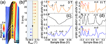
Figure 5. Valley polarisation and inversion in a graphene ripple. (a) STM image. Dots mark positions where tunnelling spectra was measured. The pseudo-magnetic field measured in the region between the two dashed curves was zero and valley-polarisation was not detected in Landau levels there. (b) Pseudo-magnetic field Bs
along the arrow in panel (a). (c) Three tunnelling spectra measured at different positions in panel (a) at  0 T. Pseudo-Landau level indexes were marked. (d) Tunnelling spectra curves measured at different positions in panel (a) at
  11 T. The indexes for the Landau levels are indicated. The subscript + (−) represents Landau levels at the
  (
( ) valley. Reprinted (figure) with permission from [112]. Copyright (2020) by the American Physical Society.
Download figure:
Standard image High-resolution imageThis effect was observed in rippled graphene grown on rhodium foil [112, 119–121]: atomically-resolved STM images along the ripple reveal compressive strains along graphene's zigzag direction (figure 5(a)). A TB Hamiltonian accounting for deformations along the ripple was used to approximate the resulting pseudo-magnetic field B s , which was non-uniform along the ridge of the ripple (dropping to zero and reversing its sign) as shown in figure 5(b).
Spectra recorded at different positions along the ripple for  T (figure 5(c)) show pseudo-magnetic Landau levels only at points where
  . The (
 pseudo-magnetic Landau levels further split in two when a magnetic field is introduced. This splitting is only seen at points along the ripple where both
B
s
and
B
R
are nonzero, in agreement with equation (29).
pseudo-magnetic Landau levels further split in two when a magnetic field is introduced. This splitting is only seen at points along the ripple where both
B
s
and
B
R
are nonzero, in agreement with equation (29).
The valley energy levels invert their energy as the pseudomagnetic field  changes sign in equation (29): beyond their valley polarisation, charge carriers also exhibit valley inversion along the ripple because
B
s
reverses sign along the y direction (figure 5(b)). This is shown at the top panel of figure 5(d): the energy levels of valley
changes sign in equation (29): beyond their valley polarisation, charge carriers also exhibit valley inversion along the ripple because
B
s
reverses sign along the y direction (figure 5(b)). This is shown at the top panel of figure 5(d): the energy levels of valley  (
( ) lie lower in energy than those of the
  valley (
 ) when
B
s
is positive.
B
s
is negative at the lower panel of figure 5(d) and the levels split again, but now the order is inverted and the LLs of the
) when
B
s
is positive.
B
s
is negative at the lower panel of figure 5(d) and the levels split again, but now the order is inverted and the LLs of the  valley appear at higher energy than those of the
  valley. The non-strained region where the
B
s
reverses its direction is not necessary to create valley polarisation, but it is critical for valley inversion.
valley. The non-strained region where the
B
s
reverses its direction is not necessary to create valley polarisation, but it is critical for valley inversion.
3.2. Graphene superlattices
The focus on this section are periodic patterns on graphene.
3.2.1. Strain-modulated superlattices.
There is a compromise between the magnitude and the spatial extent of magnetic fields at the nanoscale: fields created by large magnets tend to be homogeneous across the samples' dimensions, while inhomogeneous fields produced by micromagnets or by superconducting gates are rather weak. However, strain makes it possible to produce pseudogauge fields  that are strong and vary at nanometer scales.
For instance, strong and inhomogeneous pseudo-magnetic fields were created in graphene deposited on Cu foils in [122] (figure 6): those foils exhibit flat terraces separated by vertical steps up to  nm in height. Graphene drapes over the steps when it is grown, becoming pulled by contact forces at the terraces. This gives rise to a periodically modulated strain profile in the (vertical) draped region, and to a graphene superlattice with pseudomagnetic fields of alternating signs modelled in figure 7(a).
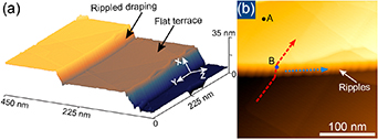
Figure 6. (a) STM topography showing draped graphene over a step separating two terraces. The draped section forms ripples due to strain. (b) STM topography around a step edge, highlighting locations at which measurements were taken. Reprinted with permission from [122]. Copyright (2020) American Chemical Society.
Download figure:
Standard image High-resolution image
Figure 7. (a) A model of Dirac electrons in an alternating magnetic field with period LB
is used to understand the  features of graphene on a draped step (figure 6). (b) LDOS as a function of LB
for
features of graphene on a draped step (figure 6). (b) LDOS as a function of LB
for  T. The black curve depicts Landau levels in graphene with energy peaks at
  . As LB
is reduced (blue trace) until it has the same order of magnitude of the magnetic length (red curve), the LDOS turns drastically different from that created by Landau levels, with peaks becoming almost equally spaced. Plots were offset for clarity. (c) and (d) Additional calculations reproduce the spatial variation of the quantised states. (c) Strained and (d) unstrained plus pseudopotential TB models capture features observed in the experimental spectroscopy along the ripple (blue arrow in figure 6(b)). Reprinted with permission from [122]. Copyright (2020) American Chemical Society.
. As LB
is reduced (blue trace) until it has the same order of magnitude of the magnetic length (red curve), the LDOS turns drastically different from that created by Landau levels, with peaks becoming almost equally spaced. Plots were offset for clarity. (c) and (d) Additional calculations reproduce the spatial variation of the quantised states. (c) Strained and (d) unstrained plus pseudopotential TB models capture features observed in the experimental spectroscopy along the ripple (blue arrow in figure 6(b)). Reprinted with permission from [122]. Copyright (2020) American Chemical Society.
Download figure:
Standard image High-resolution image
The nanometer-scale modulation of the pseudomagnetic field affects the electronic spectrum in radical ways. Indeed, the spectrum does not exhibit Landau quantisation of Dirac fermions of the form  , but to a quantisation appearing linear in energy (
 ). Although a similar type of quantisation can occur due to confinement, such explanation is discarded because the gap between peaks is independent of the ripples' wavelength [122]. Instead, calculations with a TB model indicate that this quantisation is a consequence of a pseudomagnetic field oscillating with a period LB
of the same order of magnitude than the magnetic length (
). Although a similar type of quantisation can occur due to confinement, such explanation is discarded because the gap between peaks is independent of the ripples' wavelength [122]. Instead, calculations with a TB model indicate that this quantisation is a consequence of a pseudomagnetic field oscillating with a period LB
of the same order of magnitude than the magnetic length ( ).
).
To reproduce the LDOS spectra, Banerjee et al considered both the pseudomagnetic and deformation potential fields created by the periodic strain [122]. Figures 7(c) and (d) contrast the calculated LDOS from a TB Hamiltonian considering the strained graphene system, and those based on a Dirac equation with a periodic pseudomagnetic field and electric potential of the form:


respectively. Both types of calculations showed good agreement with experimental measurements [122]. Strain patterns with alternating zones of up/down pseudomagnetic fields can create valley-Hall edge states, which could be observable at room temperature due to the pseudo-magnetic fields ( T) that can be experimentally created: graphene ripples might provide a platform for valley-dependent electron transport.
3.2.2. Inducing strain via patterned substrates.
Methods to induce pre-designed strains are highly desirable, and a promising avenue is to support graphene on patterned substrates [28, 123–126] which create a network of wrinkles (figure 8). Depending on the height-to-separation ratio of those pillars, sections of graphene might rest on the substrate, or the entire monolayer may be suspended like a canopy.
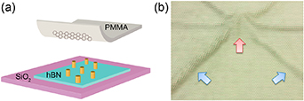
Figure 8. (a) Graphene on nanopillars. (b) Schematics of a graphene membrane supported on a pillar (red arrow) and the resulting strain-induced ripples (blue arrows). Reprinted with permission from [28]. Copyright (2017) American Chemical Society.
Download figure:
Standard image High-resolution imageEstimations of strain with a STM are usually derived from  spectra. Nevertheless, the magnifying effect of moiré patterns allowed to characterise the strain in graphene directly in [28]. The setup consisted of a gold nanopillar array over a hBN flake, which produces a moiré due to the mismatch with graphene (see figure 9). The pillar-induced strain on graphene modifies the moiré [127], making it possible to quantify the strain in graphene (whose maximum value turned out to be about
  ) with standard STM resolution. The measured strain was in agreement with estimations made from the energy separation of pseudo-Landau levels from the
  spectra. Such levels of strain would have been difficult to detect directly without the additional moiré pattern, which allowed for a 20-fold increase in atomistic precision.
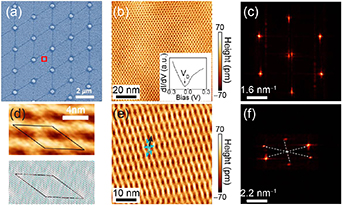
Figure 9. (a) Scanning electron microscopy image of graphene over gold nanopillars (white spots) and strain-induced ripples (lines in between nanopillars). (b) STM topography of graphene at a region away from the nanopillars. The  curve shown as an inset displays the characteristic 'V-shape' of unstrained graphene. (c) Fourier transform of the image shown in (b). The superlattice reflects a moiré pattern between graphene and an hBN flake. (d) Measured moiré pattern on strained graphene over the nanopillars (top) and simulated model (bottom). The supercell is shown in black in both panels. (e), (f) Moiré pattern and its Fourier transform on the strained graphene lattice and the hBN substrate at the position marked by the red square in (a). Arrows are the lattice vectors of the distorted graphene. Reprinted with permission from [28]. Copyright (2017) American Chemical Society.
Download figure:
Standard image High-resolution imageSimilar rectangular nanostructure arrays were used to strain graphene in [126]. There, wrinkles–quasi-1D 'channels' with a near-uniform pseudo magnetic field–developed on graphene when it was placed between two nanostructures having a critical separation. Calculations revealed that parallel arrays of those channels can be used to realise valley polarisation. Other works have studied strained graphene over SiO2 nanospheres [124], or over black phosphorus substrates [128].
3.2.3. Second harmonic generation on sublattice-polarised graphene.
As discussed in section 3.1.5, a non-zero sublattice imbalance (this is, an in-plane electric polarisation P) can be created by strain that breaks the inversion symmetry of the graphene lattice. Sublattice charge imbalance has also been verified through optical second-harmonics: the schematics on figure 10(a) show graphene on nanopillars again (see figures 8 and 9), and this sample is irradiated with a pump laser at 1035 nm. Figure 10(b) is a measure of strain through Raman spectra: according to [129], the sample is non-uniformly strained up to ∼2.4% by the nanopillar array. The temperature-dependent peak at half wavelength (1035/2 nm) displayed in figure 10(c) confirms the creation of a second harmonic on non-uniformly-strained graphene. That a pseudomagnetic field can be obtained from within atomistic displacements was stated in [102], and the fact that the polarisation differs in between lattices under anisotropic strain can be traced down to the fact that the effect on the diagonal entries of the Dirac Hamiltonian can be written as [81]:
where  and
and  .
.
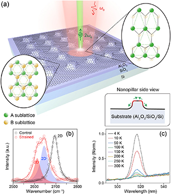
Figure 10. (a) Strained graphene on a nanopillar array gives rise to second harmonic generation. (b) The shift of Raman 2D peak verifies the strain on graphene. (c) Temperature-dependent emission at 1035/2 nm. Since the wavelength of the pump laser is 1035 nm is, emission at half-wavelength confirms the creation of SHG. Reproduced from [129]. CC BY 4.0.
Download figure:
Standard image High-resolution imageSecond-harmonic generation has also been experimentally employed to sense strain in MoS2 monolayers [130], and it is a powerful and promising technique suitable for strain characterisation of arbitrary 2D materials. More will be said on structures lacking a centre of inversion, on the existence or creation of electric dipoles, and on second harmonic generation in forthcoming pages.
3.2.4. Flat-band superconductivity in strained graphene.
The absence of superconductivity (SC) in intrinsic graphene (with its Fermi energy located at the zero-density Dirac point) is expected from the Bardeen–Cooper–Schrieffer (BCS) theory: in the limit of small DOS at the Fermi level  , that theory indicates a critical temperature depending exponentially on the coupling strength λ,
 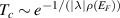 [131], and a large charge doping would be required to produce a Tc
of a few Kelvin.
[131], and a large charge doping would be required to produce a Tc
of a few Kelvin.
Because flat bands enhance electronic interactions, strained graphene can be of interest for studying many-body phases arising due to a flat electronic spectrum. Flattening of the electronic bands provides an alternative to increase the DOS and hence to induce SC, because the BCS theory leads to a linear dependence between Tc
and the coupling strength λ,  [132–134] for large
  .
.
Now, although large magnetic fields can induce flat bands (Landau levels), they also break time reversal symmetry and suppress (singlet) SC order. This is due to the Zeeman effect, which causes alignment of the electron spins and breaks Cooper pairs. Strain-induced flat bands, on the other hand, do not break time reversal symmetry and open the possibility to engineer SC [133–139]. Furthermore, one can choose the strain field's symmetry, period, and strength separately. (This situation is unlike that observed in twisted bilayer graphene (TBG), where the corresponding parameters are mostly determined by the moiré pattern. Note that flat bands can also be created in few-layer rhombohedral graphene [140].)
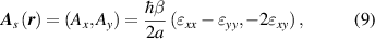
Strain-induced flat bands in graphene are due to wavefunctions localised at domain walls where the strain-induced potential changes sign [134, 141]. This permits mapping the system into a continuum Jackiw–Rebbi model with pseudo-Landau levels [141]. In fact, an exact Su–Schrieffer–Hegger (SSH) model is obtained when the momentum is set parallel to the direction of the strain modulation [134]. Interestingly, the inclusion of the electron–electron interaction leads to magnetic domains and a pairing effect [141]. A model for superconductivity in graphene with strain-induced flat bands was studied in [139], and it is discussed next. Strain was added to the low-energy dispersion of graphene via periodic (1D or 2D cosine) pseudo-vector potentials A s of period d and strain strength u0 (see equation (9)):
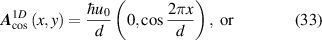
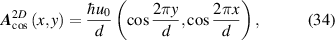
which can be realised by the following in-plane displacement fields:
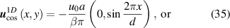
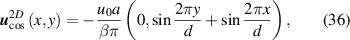
(see figures 11(a) and (b)) with β the Grüneisen parameter for graphene. The vector potentials can be obtained from these displacement fields by following equations (3) and (9), and the notation in [139] was modified for consistency with the one used here. The resulting pseudomagnetic field  is shown in figures 11(c) and (d). (The pseudomagnetic field strength (
 100 T) and period (
 14 nm) visualised in experiments [142] would lead to u0≈ 5 for the displacement fields defined here.)

Figure 11. (a), (b) Displacement fields in graphene leading to pseudo vector potentials  and
and  (the amplitudes were increased for clarity). (c), (d) Corresponding pseudomagnetic fields
  . (e), (f) Corresponding (sublattice-dependent) SC order parameter
  (A orange, B blue), which peaks at the extreme values of
B
s
. Adapted from [139]. © IOP Publishing Ltd. All rights reserved.
(A orange, B blue), which peaks at the extreme values of
B
s
. Adapted from [139]. © IOP Publishing Ltd. All rights reserved.
Download figure:
Standard image High-resolution imageThe SC state was modeled by the Bogoliubov–de Gennes mean-field theory [143] once strain was introduced, assuming an intervalley local attractive interaction leading to a s-wave pairing Δ order parameter (figures 11(e) and (f)). Critical values are studied as a function of the interaction strength. The low-energy states of strained graphene exhibit a sublattice polarisation that follows the pseudo-magnetic field and, accordingly, the SC order parameter  is sublattice-dependent.
  always peaks at the largest value of the pseudomagnetic field. This situation can be contrasted against TBG, where Δ is localised around AA stacking regions for the first-magic angle.
The electronic energy dispersion of graphene with strain fields and without them is shown in figure 12. The case with  is shown both in the mixed and reduced zone schemes for easier comparison. Substantial band flattening occurs at low energies, similar to those observed in TBG.

Figure 12. Low-energy electronic dispersion in the normal state of unstained (orange) and strained (blue) graphene for the 1D cosine potential  (subplots (a) and (b)) and the 2D cosine potential
  (subplot (c)). The dispersion arising from a 1D strain is shown in both the mixed and reduced zone schemes for better visualisation. Adapted from [139]. © IOP Publishing Ltd. All rights reserved.
Download figure:
Standard image High-resolution imageThe SC order parameter Δ exceeds the flat-band bandwidth for high enough values of the strain strength u0 and the interaction strength λ, and its dependence is linear in λ [132–134]. At lower values of u0 and λ, the dispersive behaviour of the bands becomes important and the order parameter is exponentially suppressed.
While the buckled graphene studied by Mao et al [142] is a promising platform for correlated phenomena, it is not in the flat band regime (where the linear dependence  occurs) and it would require increasing the strain strength u0 by a factor of 4 in order to lead to a SC transition at a temperature on the order of 1 K. Moreover, for this strain strength, Peltonen and Heikkilä [139] estimated a transition temperature of ≈11 K for a period d ≈ 8 nm. The calculation is done using the same λ estimated for TBG [144]. SC could still be possible for lower strain fields outside of the flat band regime, but a Tc
well under 1 K would be expected. Regardless, the possibility of having tunable SC and order parameters via strain is attractive, and the generality of the model might be of relevance in the study of SC in other graphene systems like TBG–where intrinsic strain is always present (more on this later).
occurs) and it would require increasing the strain strength u0 by a factor of 4 in order to lead to a SC transition at a temperature on the order of 1 K. Moreover, for this strain strength, Peltonen and Heikkilä [139] estimated a transition temperature of ≈11 K for a period d ≈ 8 nm. The calculation is done using the same λ estimated for TBG [144]. SC could still be possible for lower strain fields outside of the flat band regime, but a Tc
well under 1 K would be expected. Regardless, the possibility of having tunable SC and order parameters via strain is attractive, and the generality of the model might be of relevance in the study of SC in other graphene systems like TBG–where intrinsic strain is always present (more on this later).
Correlations were introduced in a similar model of periodically strained graphene via a spatially-dependent antiferromagnetic coupling [138], showing that a chiral, d-wave SC can be stabilised via strain as well.
3.2.5. Flat electronic bands and electron-electron correlations in buckled graphene.
It was just argued that flat bands are a necessary ingredient to create superconductivity in graphene. Additional approaches to achieve flat electron bands are arising because of that.
Stiff membranes can undergo a buckling transition when exceeding a critical value of in-plane compressive strain (because out-of-plane distortions reduce the elastic energy of the membrane). Those distortions lead to periodic strain patterns, which in turn create periodic pseudomagnetic fields that (as seen in the previous section) can give rise to flat electronic bands [142].
Triangular buckling patterns consisting of alternating crests and troughs have been observed in graphene deposited over NbSe2 [142]. Those superstructures had a height modulation of 0.17 nm and a period of about  nm. A schematic of buckled graphene is shown in figure 13(a). In the crest regions, the
  spectra exhibited peaks that were identified as the pseudo-Landau levels induced by a pseudomagnetic field Bs
(
spectra exhibited peaks that were identified as the pseudo-Landau levels induced by a pseudomagnetic field Bs
( for
for  ), confirming the existence of a pseudo-magnetic field with a magnitude of about
  T. Furthermore, sublattice polarisation, a hallmark of the wavefunction of the n = 0 pseudo-Landau level, was visualised through STM measurements at crests and troughs [142]. The sublattice polarisation (A or B) seen in the STM measurements changes when moving from a crest to a trough, indicating a change in the sign of Bs
between these two regions (there was no sublattice polarisation at the interface between crests and troughs, indicating that
T. Furthermore, sublattice polarisation, a hallmark of the wavefunction of the n = 0 pseudo-Landau level, was visualised through STM measurements at crests and troughs [142]. The sublattice polarisation (A or B) seen in the STM measurements changes when moving from a crest to a trough, indicating a change in the sign of Bs
between these two regions (there was no sublattice polarisation at the interface between crests and troughs, indicating that  there).

Figure 13. (a) Buckled graphene with pseudomagnetic field Bs indicated in false colour. (b) The local density of states shows the formation of an effective, large-scale honeycomb lattice. Valley-projected band structure of the graphene superlattice across a path in the mini-Brillouin zone (c) without strain, and (d) with buckling-induced strain. Reprinted with permission from [145]. © IOP Publishing Ltd. All rights reserved.
Download figure:
Standard image High-resolution imageThe  spectra and the pseudo-Landau levels were described by a TB model of graphene in the presence of a periodic pseudo-magnetic field with triangular symmetry [142]:

where B is the amplitude of the pseudo-magnetic field, ab
the superlattice period, 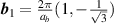 ,
,  and
and  . The choice of coordinates is consistent with C6 symmetry and with the fact that the total pseudo-magnetic flux has to vanish (since time-reversal symmetry is not broken by strain). When the sample is doped to partially fill the n = 0 pseudo-Landau level, a pseudo-gap feature splits the peak in two, indicating the appearance of a correlation-induced state. Moreover, a spectral weight redistribution between the two peaks is observed when doping away from charge neutrality. Similar signatures have been observed upon partially filling the flat band of magic-angle TBG.
Milovanović et al studied the flat bands in periodically buckled graphene [146] considering three different geometries: a triangular pseudo-magnetic field mode (experimentally observed in [142]), a hexagonal buckling mode (which leads to a pseudo-magnetic field similar to the ones obtained for gaussian bumps and bubbles), and a herringbone buckling mode corresponding to an undulating 1D strain pattern. The herringbone buckling has the lowest energy of those three configurations at large strain.
The amplitudes and periods of pseudo-magnetic fields required to access correlated phases were ascertained by comparing the bandwidth  to the characteristic energy scale for the interactions, EI
. The critical pseudo-magnetic field takes this form when employing the triangular pseudo-magnetic field mode [146]:
to the characteristic energy scale for the interactions, EI
. The critical pseudo-magnetic field takes this form when employing the triangular pseudo-magnetic field mode [146]:

at which  for the nth band. Φ0 is the magnetic flux quantum and S is the area of the unit cell. In the triangular pseudo-magnetic field mode,
  for the lowest band. For the next band
  . Because higher bands have smaller bandwidths and are also gapped, they might also be relevant for studies of correlated phenomena.
Bands are not as flat in the hexagonal buckling mode: broader LDOS peaks indicate that this pseudo-magnetic field cannot localise electrons efficiently. Similarly, the herringbone mode does not exhibit a gap opening nor flat bands, even for strains as large as 20 . This is a consequence of this buckling mode being the lowest-energy configuration: the average strain in the herringbone mode is generally half of that displayed in the hexagonal mode (and its pseudo-magnetic field is even an order of magnitude smaller).
Buckled graphene superlattices do not localise charge carriers fully. Spatial regions in between those undergoing large pseudo-magnetic fields turn into percolating paths, along which charge carriers propagate. This is seen in the longitudinal conductance, which shows peaks coinciding with the LDOS [146] and confirms the non-localised nature of flat band states.
Electron–electron interactions were introduced by a Hubbard term in a TB model for buckled graphene [147]:
while strain was introduced by modifying the hopping energies connecting the three nearest neighbours  (
( ) with
and the model was solved with the non-collinear mean field formalism for U = t [147].
They found correlated states at values close to  . While the system remained gapless in the non-interacting case, an emergent magnetic state with a non-homogeneous magnetisation and a correlation gap of
  (consistent with experiment [142]) was obtained when interactions were turned on. The correlated state is not expected to arise for pristine graphene at the same value of U. The strain-induced band flattening is essential for such magnetism to emerge, because it creates a bandwidth
  smaller than the Hubbard interaction U (
 ). The periodic magnetisation patterns give rise to an emergent honeycomb superlattice with antiferromagnetic ordering. The regions of highest LDOS can be understood as Wannier orbitals, and the sign of the net magnetisation at a given region follows the sign of the pseudo-magnetic field. The magnetic ordering decays as the system is doped away from half filling, a result consistent with experiment [142].
Because of the strain-induced crests and troughs in the superlattice, an electric field impinging along the z-direction can induce non-homogeneous local energy shifts, which are modeled via height-dependent onsite energies  in the TB Hamiltonian. This term creates sublattice imbalance in the emergent honeycomb superlattice, and competes with the magnetic ordering, thus holding potential for electrically tuning the magnetic ground state, and for exploring the interplay between strain-induced gauge-fields and electron-electron interactions.
Manesco and Lado [145] derived an effective model for the emergent honeycomb lattice that arises in buckled graphene (figures 13(a) and (b)). The minima and maxima of  contain the highest LDOS, and were considered as Wannier orbitals. The effective TB model for the emergent honeycomb lattice includes sublattice imbalance and a valley-dependent, second-nearest neighbour hopping. Remarkably, such model turns out to be fully analogous to the Kane–Mele model for a spin quantum Hall insulator [148, 149]. Here, the valley isospin plays the role of spin, and the superlattice's mini-valleys play the role of the valleys. Due to the height variation in the buckled graphene, out-of-plane displacement fields increase (or decrease) the energy of states at the
  maxima (minima). In the effective model, this is equivalent to increasing the sublattice imbalance, which in turn acts as a knob to tune the system's topology.
Onsite and nearest neighbour Hubbard terms were part of the effective model (with interaction strengths U and V, respectively), and a mean field approach was used. Two different ground states (a charge density wave and an antiferromagnetic state) were found at different values of U and V [145]. Each ground state creates different sublattice imbalances and, as in the Kane–Mele model, this leads to topological transitions.
Indeed, the valley Chern number was calculated for different values of the interaction-induced sublattice imbalance, and both the charge density wave and antiferromagnetic phases in the interacting phase diagram can be further divided into topologically trivial and nontrivial phases. Analogous to the Kane–Mele model, the non-trivial phases are quantum valley Hall insulators that exhibit counter-propagating edge states with opposite valley polarisation. Edge states are further spin-polarised in the topologically non trivial antiferromagnetic phase.
A closely related phenomena is the curvature-induced spin-Hall effect in a graphene Möbius strip. The solution of the Dirac equation shows that despite the absence of a Hall current, a spin-Hall current is a natural consequence for such a topology [53]. Other works have studied topological phases arising from strain and its interplay with interactions in graphene [100, 116, 136, 150–152]. Buckling was also shown to allow control of topological edge states via electric fields in germanene [153].
The results within this subsection place buckled graphene at the interface of strain, flat bands, correlations, and valley topology.
3.2.6. Adatom-induced graphene superlattices.
Massive and massless charge carriers were observed on caesium-doped graphene; a system modelled as a strained quantum well [154]. Extended flat bands were reported for this system in a later work [155].
3.2.7. Short-wavelength periodic lattice deformations: Kekulé and other  patterns.

Adatoms within substrates, localised mechanical probes, and electron-electron interactions induce short wavelength lattice modulations on graphene [156]. This subsection is focused on the paradigmatic case of Kekulé patterning observed on graphene deposited over a Cu(111) single crystal (and dubbed Kek-Y) [157] and on Li-intercalated graphene (Kek-O) [158]. As depicted in figure 14 by bonds of two different strengths, Kekulé patterns have few hopping strengths changed within a  periodic supercell (shown by dashed lines within the figure). Two Kek-Y structures–related by a reflection with respect to the vertical line–are shown in figure 14 as well [159].
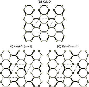
Figure 14. The Kek-O (subplot (a)) and two possible Kek-Y honeycomb structures (subplots (b) and (c)): as schematically indicated by thicker or thinner lines, bond strengths are different. The  unit cells were drawn with dashed lines. The two Kek-Y structures are related by a reflection with respect to a vertical line.
Download figure:
Standard image High-resolution imageA study on strongly-interacting electrons in hexagonal lattices [160] will be highlighted now. Figure 15 presents graphene (a semimetal (SEM): this is, an electronic system with interactions turned off), an antiferromagnetic insulator (AFI), the Kek-O superlattice (renamed as 'dimerized insulator' (DIM) in [160]), and a lattice with a hexagonal distortion (dubbed HEX). Those will turn out to be competing phases on the honeycomb lattice.

Figure 15. Competing phases when electron-electron interactions and deformations are included: (a) semimetallic (SEM) graphene, (b) honeycomb antiferromagnetic insulator (AFI), (c) Kek-O or dimerised Kekulé-like insulator (DIM), and (d) distorted hexagonal (HEX) insulator. The labels tA , tB and tC are hopping integrals for the corresponding TB models used in the kinetic part of a Hubbard Hamiltonian that includes the elastic energy due to elastic distortions given in equation (41). Reprinted (figure) with permission from [160], Copyright (2018) by the American Physical Society.
Download figure:
Standard image High-resolution imageOne sets graphene onto a Hubbard model Hamiltonian with an additional elastic energy term [161]:
The  on equation (41) are fermion annihilation operators at lattice site x with spin σ. The occupation number of such site is
  . The on-site repulsion U can have any sign as long as it is the same for all lattice sites. The first nearest-neighbour hopping integrals
  between sites x and y are real, as there is no magnetic field, and are assumed positive although not necessarily independent of the
  pair (x and y here do not denote Cartesian components but different sites within the Honeycomb lattice). The TB parameters txy
depend on the physical distance rxy
between the lattice sites x and y, and are usually assumed to decay exponentially [1].
pair (x and y here do not denote Cartesian components but different sites within the Honeycomb lattice). The TB parameters txy
depend on the physical distance rxy
between the lattice sites x and y, and are usually assumed to decay exponentially [1].
The main addition in equation (41) with respect to equation (39) is the elastic distortion energy  , which makes the updated Hamiltonian depend on the distortions of the lattice. The configurations
  that minimise the ground state energy, including all periodic, nonperiodic and chaotic structures depend on a Peierls-type of instability of the bond lengths similar to the one employed in the archetypical polyacetylene chain model [162, 163]–also known as the SSH model.
Frank and Lieb demonstrated that only periodic, reflection-symmetric distortions are allowed on the  supercell [161] in the thermodynamic limit, and figure 15 presents all the possible structures satisfying such criterion.
A phase diagram based on (quantum) Diffusion Montecarlo (DMC) simulations is provided in figure 16 [160]. The figure presents a comparison between the ground state energies of the competing phases seen in figure 15 for isotropically strained graphene, as obtained from DMC and DFT, and it also includes the magnitude of the enthalpies when the lattice is under stress. DMC produces the lowest enthalpy when compared to unperturbed graphene. For uniform graphene strain in the 7%–15% range (corresponding to a  –31 N m−1 stress), the lattice correlation-driven dimerisation freezes Pauling's resonating valence bond into a valence-bond solid realised by an insulating Kekulé-like dimerised phase (DIM) [160, 164, 165] that creates a topological band gap opening in isotropically strained graphene. Kekulé patterning has been observed by STM in strained graphene [166], and it seems to play a role in the superconducting phases of TBG [165, 167, 168].

Figure 16. (a) Ground state energy E relative to graphene's (SEM) energy  versus strain ε. The trends were obtained by DMC and DFT for the insulating Kekulé like dimerised (DIM), antiferromagnetic insulator (AFI), and the distorted hexagonal insulator (HEX) phases. (b) Stress (σ)-strain (ε) relation for strained graphene obtained by fitting DMC energies. Dashed lines mark the transition stress values for the SEM-DIM transition. (c) Enthalpy H of strained graphene relative to the SEM phase
  versus tensile stress σ. The blue-shaded region indicates the error bars on the enthalpies for DIM and AFI phases by DMC. Reprinted (figure) with permission from [160], Copyright (2018) by the American Physical Society.
Download figure:
Standard image High-resolution imageStrong magnetic fields can also create Kekulé distortions in graphene: Using scanning tunnelling spectroscopy (STS), a continuous quantum phase transition from a valley-polarised state onto an intervalley coherent state with a Kekulé distortion was observed under magnetic fields [169]. Importantly, the valley texture extracted from STS measurements of the Kekulé phase revealed valley skyrmion excitations localised near charged defects [169].
Gamayun et al obtained a low-energy four band model from the complete six-band TB model for both Kek-O and Kek-Y patterns without strong electron-electron interactions [159]. Some features of the Y Kekulé pattern will be discussed next.
Pristine graphene and a structure hosting a Kek-Y pattern–indicated by red and black bonds–are shown in figures 17(a) and (b), respectively. As indicated in figure 14, the Kek-Y unit cell contains six atoms and lattice vectors  and
and  in figure 17(b). The corresponding reciprocal lattice vectors are scaled as
  [170].

Figure 17. Effect of strain on a Kekulé distorted lattice. Lattices in real space, first Brillouin zones, and energy dispersion for: (a) pristine graphene, (b) Kek-Y distorted graphene, (c) strained graphene, and (d) Kek-Y distorted graphene with strain. The Kekulé and strained Kekulé vectors G and  are indicated in the upper side of the hexagonal first Brillouin zones. In (a), the Dirac cones are shown in dark gray. In (b), the gray Dirac cones are folded into a degenerate (blue) Dirac cone to the Γ point. In subplot (c), the original Dirac cones (in gray) are deformed and translated to the (red) points
  . Dirac cones (gray) are folded into the Γ point in panel (d). Strain breaks the degeneracy resulting in an overlap of the two shifted Dirac cones, indicated in purple. Reprinted (figure) with permission from [171]. Copyright (2019) by the American Physical Society.
Download figure:
Standard image High-resolution imageThe system is modelled by a TB Hamiltonian with one π-orbital per carbon atom [1]. Going beyond first-nearest neighbour hopping [159], a second-nearest neighbour TB Hamiltonian was employed [172]:
where  and
and  are annihilation operators at site r for a carbon atom in the A or the B sublattice, respectively. Operators
  and
and  are the corresponding creation counterparts. A bond-density wave modulates the TB parameters and originates the Kekulé distortion: the first-neighbour hopping is given by [159]:

where  eV is the hopping parameter for first-nearest neighbours in pristine graphene and
  is a reciprocal lattice vector coupling both valleys (see figure 17(b)). The amount of the bond modulation was
  . In addition, p and q are two integers such that the index:

distinguishes the Kekulé O pattern (ν = 0) from the two Y patterns ( ) alluded to in figure 14.
The subsequent, second-nearest neighbour parameters were periodically modulated as:

where  is the second-nearest neighbour TB parameter of pristine graphene.
A column vector is now defined:
that collects annihilation operators at k and  , so that the Hamiltonian can be written as a
  matrix:
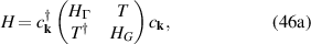
made from the original graphene Hamiltonian at the  point:

the Hamiltonians at the G and  points:
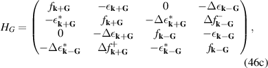
and the interaction between them:
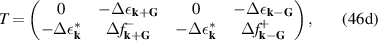
where
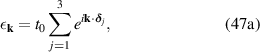

The spectrum can be found by diagonalisation of the  operator or by a projection technique that permits obtaining a low-energy
  matrix effective Hamiltonian. That effective Hamiltonian becomes for the Kek-Y case [172]:
where  and
and  are two vectors with components defined from Pauli matrices, σ0 and τ0 are two
  identity matrices, and µ is defined as:
The resulting four low-energy bands turn out to be:
were two new velocities have been defined:  , and
, and  .
.
As indicated in figure 17(b), the Kek-Y pattern folds the two valleys  and
and  into the Γ point when
  . One valley is a fast Dirac cone with Fermi velocity vM
, and the other a slow Dirac cone with Fermi velocity vD
. Specific signatures on the optical and electrical conductivities, as well as in plasmons, are associated with those two charge carrier flavours [170, 173, 174]: the valley-dependent splitting of the Fermi velocities due to the Kekulé distortion leads to a similar splitting in the dielectric spectrum [173]. Moreover, an absorption phenomenon was found where a resonance peak related to intervalley transport emerges at a 'beat frequency' determined by the difference between characteristic frequencies of each valley [173].
. One valley is a fast Dirac cone with Fermi velocity vM
, and the other a slow Dirac cone with Fermi velocity vD
. Specific signatures on the optical and electrical conductivities, as well as in plasmons, are associated with those two charge carrier flavours [170, 173, 174]: the valley-dependent splitting of the Fermi velocities due to the Kekulé distortion leads to a similar splitting in the dielectric spectrum [173]. Moreover, an absorption phenomenon was found where a resonance peak related to intervalley transport emerges at a 'beat frequency' determined by the difference between characteristic frequencies of each valley [173].
Kekulé-patterning was observed in a work that combined STM and DFT calculations for both graphene monolayers and bilayers [175]. It was shown that strain induced a splitting of the Dirac cones and a band gap (it is not clear if the mechanism is the one predicted in [171] though). Flat bands measured with ARPES were shown to coexist with the bond order in Li-intercalated graphene [176].
The inclusion of second-nearest neighbour hopping changes this picture slightly, as one of the cones gets a small mass [172]. In a similar way, a gap opens in the energy dispersion for the Kek-O pattern [159]. Such band gap was experimentally confirmed by strain-induced Kekulé patterning [166].
Uniform strain has been proposed as a tool to engineer the valley degree of freedom [171]: while valleys are too far away to mix under realistic strain in pristine graphene [1], the folding induced by patterning reduces the separation between them, so that strain can modulate their interactions more easily.
As seen in figure 17(c), uniform strain moves the  points to
  in graphene [1]. Moreover, strain changes the symmetry of the Bravais lattice, and high-symmetry points of the reciprocal lattice must be labelled differently. As an example, the
  points of the P6/mmm space group are replaced by the F0 and Δ points in the Cmmm space group when under uniaxial strain, and the Dirac points
  of the strained lattice do not necessarily coincide neither with
  , nor with F0 or Δ. Figure 17(c) sketches those general observations to avoid confusion.
Uniform strain in Kekulé patterned graphene leads to the situation depicted in figure 17(d): the original valleys are folded into new cones located at  and
and  . These new Dirac points are very close to the Γ point, and their separation can be tuned by experimentally accessible strain [171] to enhance valley interactions.
3.2.8. Time-dependent strain.
In analogy to electromagnetic fields, strong time-dependent gauge fields can be generated by time-varying strain in graphene. Time-dependent deformations can be induced by local probes such as a transmission electron microscope (TEM), or by SAWs created at a proximal piezoelectric layer [4].
The possibility of controlling electron transport by time-dependent gauge fields was suggested in [1, 177], and phonons were seen to generate effective pseudoelectromagnetic waves [60, 177]. Since then, acoustic waves have been shown to induce a giant synthetic Hall voltage without external magnetic fields [4], and the experimental setup is depicted in figure 18(a): graphene lays on top of LiNbO3, which itself lays on an insulating SiO2 substrate, which sits on a p-doped silicon wafer. The carrier concentration is tuned by a voltage VBG
applied to the  doped substrate.
Figure 18. Synthetic Hall voltages in graphene by acoustic waves. (a) Top: Raman spectra of graphene (MLG). Inset: diagram of graphene on substrate. Carrier concentration was tuned by a voltage VBG
applied to the p-doped substrate. Bottom: two measurement configurations. In the magnetotransport configuration, a constant current I is passed through the Hall bar. In the acoustic transport configuration, a microwave frequency is applied to the inter-digitated top contacts (IDT) and the resulting acoustic current,  , is measured in a short-circuited configuration. (b) A typical magnetotransport measurement for
  V for the Hall resistivity Rxy
and magnetoresistance Rxx
versus magnetic field B. The inset is carrier density versus
VBG
. (c) In the acoustic measurement,
V for the Hall resistivity Rxy
and magnetoresistance Rxx
versus magnetic field B. The inset is carrier density versus
VBG
. (c) In the acoustic measurement,  as a function of frequency, power and VBG
for the fundamental resonance of the IDT. Data were obtained at 4.2 K. Reprinted (figure) with permission from [4]. Copyright (2022) by the American Physical Society.
as a function of frequency, power and VBG
for the fundamental resonance of the IDT. Data were obtained at 4.2 K. Reprinted (figure) with permission from [4]. Copyright (2022) by the American Physical Society.
Download figure:
Standard image High-resolution imageThe device can interchangeably be used in a magnetotransport Hall configuration under a real magnetic field B, or in an acoustic transport configuration. In the latter configuration, acoustic waves are induced in the graphene by an interdigitated resonator. Figure 18(b) displays a typical Hall measurement with Hall resistivity Rxy
and magnetoresistance Rxx
. The plateaus in Rxy
indicate the presence of a quantum Hall effect. Figure 18(c) presents the acoustic induced Hall effect, seen in the current  .
.
SAWs can also provide alternative ways to study topological properties [178–180] and the topological non-adiabaticity at the Dirac point [181]. The issue at hand is that the main assumption of topological phases is the adiabaticity of the time-dependent change of external parameters of a quantum system, which could require a bigger bandgap than the energy provided by external probes. However, there is no bandgap in Dirac materials, and transitions are induced at all frequencies. This produces a region of non-adiabaticity around the cones that requires additional theory to be properly understood [181–183].
Extensions to the strain engineering of other 2D Dirac semimetals–which might be more sensitive than graphene and could thus function as strain sensors–are underway [184].
3.2.9. Berry dipole and nonlinear transport from strain.
Strain can also appear in the non-linear conductivity of gapped graphene [185].
When both time reversal and inversion symmetry are present, these higher order phenomena vanish because the Berry curvature Ω is zero [186].
Thus, breaking of inversion symmetry becomes necessary [187] if no magnetic field is present (i.e. when graphene's Hamiltonian is invariant under time reversal). If space symmetries are further reduced by strain, the Berry curvature becomes asymmetrical in reciprocal space, and the integral  (the so-called Berry dipole, with f0 a Fermi–Dirac distribution) turns nonzero. Sodemman and Fu [188] have shown that (under time-dependent bias) the Berry dipole contributes to the second order conductivity in the direction normal to the bias, that is, in the same way as the Hall effect, the resulting second order transversal conductivity tensor being proportional to the Berry dipole.
The stretching of the crystal structure (as a consequence of strain) implies the reduction in the number of crystal symmetries of the lattice. In Bernal-stacked bilayer graphene under a normal electric field, or in graphene on top of hBN, sublattice equivalence is broken and so is inversion symmetry, reducing the symmetry from  to
to  . Uniaxial strain reduces the symmetry further, from
  to
to  [189]. When combined with the wrapping of the bands, this leads to an effective Hamiltonian with a nonzero Berry dipole [190].
3.3. Experimental verification of a tunable electronic topology in germanene
The discussion continues with germanene, another monoelemental 2D material with a honeycomb lattice, because of the very recent experimental verification of its tunable topological properties [153]. Its availability opens possibilities for topological field-effect transistors whereby a back or top gate turns dissipation-less transport along its edge on and off [148].
Unlike silicene [191, 192], 2D germanium stabilises on a hexagonal closed packed bilayer structure with ninefold coordination [191, 193, 194]. Nevertheless, it does form a low-buckled hexagonal configuration when grown on either gold(111) [195] or Ge2Pt(101) [153] substrates.
There are advantages in growing germanium on Ge2Pt(101) though [153]. The most salient one is the creation of a buffer layer reminiscent of that created in epitaxial graphene grown on silicon carbide [196], which renders a graphene-like dispersion on the next subsequent carbon layer. Here, a second layer above appears electronically and chemically decoupled, thus featuring the electronic and topological properties predicted in freestanding germanene [191]. In particular, a spin–orbit-coupling-induced band gap of 23.9 meV, which is sufficiently large to observe the Quantum Spin Hall effect. Experimentally, the observed gap was much larger at 70 meV; this discrepancy may be due to strain, buckling [43], stacking sequence, and effects due to the proximity to the substrate.
3.4. Piezoelectricity by strain in hexagonal boron nitride monolayers
An essential feature of noncentrosymmetric crystals is piezoelectricity, which permits exchanging strain and intrinsic (internal) electric fields. The induced charge density ρ couples to strain through variations in the intrinsic polarisation P through [197]:

The ith-component of the intrinsic polarisation P couples to the crystal strain through:
where γijk
is the 3rd rank piezoelectric tensor, whose only non-zero entry is  for 2D materials with
  symmetry. This way, it can be shown that
  , where
  , with
  ,
,  , and
, and  . The piezoelectric coefficient is estimated to be
  C m−1 using the modern theory of polarisation, working with a two-band model of a massive Dirac equation with a 5.97 eV band gap [35].
Electrical measurements performed by electrostatic force microscopy on top of bubbles and creases of hBN monolayers (figure 19) show a net electric field, which in turn represents another method to quantify local strain [35]. (Electrostatic force microscopy is a non-contact technique that maps the local electrostatic interaction a tip and a sample.) No such contrast was observed on hBN bilayers nor in bulk samples, which recover a centre of inversion despite strain.

Figure 19. (a) Topography and (b) electric images of a hexagonal boron nitride monolayer triangular bubble. (c) Profiles along the lines in (a) and (b) and in a corresponding dielectric image. (d) Simulated topography image and corresponding (e) electric-field energy density and (f) polarisation. Reproduced from [35]. CC BY 4.0.
Download figure:
Standard image High-resolution image3.5. Quantifying strain on transition metal dichalcogenide (TMDC) monolayers
TMDCs transition from an indirect onto a direct band gap at monolayer thickness. They display multiple electro-optical properties [198], including strong exciton binding energies and photoluminiscence, that can be tuned by strain.
Quantitatively assessing the degree of strain, nevertheless, is not a trivial task. The difficulty stems from the fact that x-ray diffraction (XRD)–the most powerful technique to measure precise lattice constants–is not readily applicable to monolayers not having a macroscopically uniform in-plane orientation. This is because the incident x-ray will spread over a macroscopic distance (of the order of millimeters) for a grazing-incidence XRD geometry required to probe any in-plane strain (figure 20), thus leading to a small averaged signal for a sample with small size and/or random orientation.

Figure 20. Superlattice strain of WSe2 monolayer on graphene measured by grazing-incidence in-plane XRD. (a) Schematic diagram of the grazing-incidence XRD geometry.  is the incidence angle of the x-ray beam. (b) Low energy electron diffraction (LEED) image taken after the growth of WSe2 monolayer on graphene. The two primary in-plane lattice spacings are highlighted. (c) In-plane δ-θ scans along two distinct crystallographic directions (Q
 SiC[
SiC[ ] and SiC[
 ]). (d) Schematic diagram showing superlattice matching between 3×3 WSe2 monolayer and
  graphene. A slight lattice compression (−0.19%) of the WSe2 monolayer enables the commensurate matching. Reproduced from [32]. CC BY 4.0.
Download figure:
Standard image High-resolution imageSubstrates can impose a uniform strain in the film grown on the surface. In standard epitaxial growth, substrates are chosen so that their surfaces have the same in-plane lattice symmetry as the film to be grown. In this case, strain is caused by the difference in the in-plane (super)lattice spacing of the substrate and the film. Synchrotron-based grazing incidence XRD was used to measure such strain in a WSe2 monolayer epitaxially grown on graphene, where a lattice compression of −0.19% was found in WSe2 [32] (figure 20). The  unit cell of the slightly compressed WSe2 was perfectly commensurate with a
  graphene lattice with a experimental mismatch below 0.03%, which could explain why the WSe2 monolayer was compressed on graphene.
As indicated in section 3.2, non-uniform strain may be realised by patterned structures manufactured on substrates. For the sake of quantitative evaluation, XRD can be applied more accurately under uniform strain conditions. Non-uniform strain, on the other hand, can be characterised with local probes such as Raman spectroscopy. In that case, the expected shift of phonon frequencies as a function of strain should be available, at least theoretically, to convert observed shifts in Raman modes into a magnitude of strain. As seen in figure 21 and similar to graphene (section 3.2.3), non-uniform strain can be measured through second harmonic generation when inversion symmetry is removed by strain [130] as well.

Figure 21. Determination of strain by second harmonic generation on a MoS2 monolayer: the arrows indicate the strain field. A SEM image is shown as an inset. Reproduced from [130]. CC BY 4.0.
Download figure:
Standard image High-resolution imageShifts as large as ∼100–200 meV in excitonic emission energies have been reported in experiments where mechanical strain is applied to TMDC monolayers, which corresponded to maximum strain levels of 1%–2% [199–204], as evaluated by Raman spectroscopies via the softening of specific Raman-active phonon modes (figure 22). For example, MoS2 monolayers experienced strain-induced softening of 1.7–2.1 cm−1/% for the  phonon mode [203, 205].

Figure 22. Strain dependence of exciton transition energy as well as Raman shifts (out-of-plane A1g mode) for MoS2 and MoSe2 monolayers. Solid and dashed lines are linear fits to the data from mechanically-strained monolayers [203, 205] and theory [206], while filled squares denote those for PVD-grown monolayers on Si3N4 (blue square) and SiO2 (orange square) in which strain is due to thermal expansion mismatch induced after the high-temperature growth. Grey lines are linear fits to data from strained PVD monolayers.
Download figure:
Standard image High-resolution imageUsing methods such as local heating, strain induced on amorphous substrates by a thermal expansion mismatch has been studied [207]. CVD-grown MoS2 monolayer is also seen to be strained after the cool down from growth at high temperatures [208]. The (per cent) strain induced in the TMDC monolayer in the latter scenario can be estimated by:

where  is the thermal expansion coefficient of a TMDC monolayer,
  is that of the substrate,
  (where
  and
and  denote the growth temperature and room temperature, respectively). Recently, strain in TMDC monolayers was enhanced by utilising a high growth temperature in PVD (
 C) and a systematic change in strain levels for Si3N4 and SiO2 substrates, consistent with the above scenario, was observed by using PL and Raman spectroscopy. The resultant strain caused large shifts in the excitonic transition energy of ∼80 meV for MoS2 monolayers on SiO2 (figure 22).
Similar to graphene and hBN monolayers, TMDC monolayers can also be strained by polymer encapsulation [15, 16], dielectric nanopillars [29, 31, 209, 210], nanobubbles [36–38], and nanoindentation [10]. Nevertheless, and in contrast with graphene, metal nanogaps [211], metal nanostructures [212], and optical waveguides [213–216] are also employed to create strain and/or to enhance their optical response. An additional pathway for strain and the tuning of optical properties is the creation of lateral heterostructures [20–24].
3.5.1. Tuning optical properties of TMDC monolayers by strain.
2D semiconductors are an important platform for the emission of light because of the reduced dielectric screening in two dimensions, the intrinsic absence of total internal reflection within their atomically-thin thickness [217], and because local tensile strain is the only mechanism to move through space (i.e. to funnel) charge neutral electron–hole pairs (i.e. Wannier excitons, or excitons for short) created in monolayers [218, 219]. Furthermore, the deterministic and position-dependent creation of few or single photons is one of the main goals of this field of research (see, e.g. [210]). A recent review on this subject is available [220], and the following paragraphs are mainly an update. A discussion of semiconducting TMDCs monolayers under strain follows, while TMDC monolayers encapsulated within a van deer Waals heterostructure are the subject of section 4.6.
Electron and hole effective masses are comparable in excitons, which makes those oppositely-charged quasiparticles wander for long distances until they break apart as they collide with phonons. The collision processes (and crystal imperfections), combined with exciton-polariton excitations give rise to a broad optical emission spectrum aided by multiple successive exciton creation and reabsorption events. Such broad emission spectrum is customarily known as photoluminiscence [221] and most experimental studies to be described now will be based on this optical technique. Importantly, the photoluminiscence spectrum depends on the quality (impurity density) of the semiconductor or insulating 2D material.
Mukherjee et al placed a WSe2 monolayer over a regular array of nanopillars separated by 4 µm and having heights of 100 nm. They observed a strain gradient in the vicinity of nanopillars, which periodically localises bright excitons in the WSe2 monolayer at 4.2 K [29]. As confirmed by auto-correlation measurements with a Hanbury–Brown–Twiss interferometer, localised emission lines turned out to be sources of quantum light. The need for spectral control of the emitted light calls for the encapsulation of the WSe2 monolayer within a van der Waals stack, and those results will be discussed in section 4.6.
Strain and defect engineering were simultaneously pursued in an effort to increase operating temperatures, photon yield, and purity of single-photon emitters on WSe2 monolayers by Parto et al [222]. Those emitters show biexciton cascade emission, single-photon purity above 95%, and working temperatures up to 150 K [222].
As depicted in figure 23(a), the spin–orbit coupling in TMDC monolayers splits the conduction band with an optical dipole-allowed bright exciton, but it also leaves the possibility of creating a (spin-forbidden) dark exciton transition at the K and Kʹ points [223–227]. In this context, the bright excitons correspond to a transition among states of the same spin, while the dark excitons correspond to transitions between states with opposite spins. In general terms, a 'dark' exciton is a light excitation requiring additional perturbations–the spin-flips described thus far, and/or momentum transfer [228]—to occur.
Figure 23. (a) Band diagram of a WSe2 monolayer with (spin-allowed) bright (X0) and (spin-forbidden) dark exciton (XD
) states.  is the spin-split energy difference at the conduction band. (b) Schematics of tip-enhanced photoluminescence with a cantilever gold tip. The bottom and tip metals create a Purcell (optical resonance) effect. (c) Bright exciton and (d) dark exciton intensities. (e) Average cross-section of intensities and strain for blue dotted regions in (c) and (d). (f) Increasing bright (X0) and dark (XD
) emission under tensile strain from data shown in (e). (g) Average cross-section of intensities and strain for red dotted regions in (c) and (d). (h) Increasing bright (X0) and dark (XD
) emission under compressive strain. Adapted with permission from [38]. Copyright (2023) American Chemical Society.
is the spin-split energy difference at the conduction band. (b) Schematics of tip-enhanced photoluminescence with a cantilever gold tip. The bottom and tip metals create a Purcell (optical resonance) effect. (c) Bright exciton and (d) dark exciton intensities. (e) Average cross-section of intensities and strain for blue dotted regions in (c) and (d). (f) Increasing bright (X0) and dark (XD
) emission under tensile strain from data shown in (e). (g) Average cross-section of intensities and strain for red dotted regions in (c) and (d). (h) Increasing bright (X0) and dark (XD
) emission under compressive strain. Adapted with permission from [38]. Copyright (2023) American Chemical Society.
Download figure:
Standard image High-resolution imageIn the WSe2 monolayers studied by Hasz et al, the dark exciton has a lower energy ( meV) than that of the bright exciton [38]. Dark excitons have a longer radiative lifetime than dipole-allowed bright excitons due to their spin- (and/or momentum) forbidden transitions [38, 229] and hence may function as coherent two-level quantum systems, or as Bose–Einstein excitonic condensates.
Excitonic states can be resonantly enhanced by the use of an AFM metallic tip sampling with a metal surface underneath (figure 23(b)) through the Purcell effect [38], which is the resonant increase of the spontaneous emission rate usually created within a cavity [230]. This technique is especially insightful to scan the photoluminiscence created at defects, grain boundaries, edges, nanobubbles (see figures 23(c) and (d)), and under uniform strain [231]. Additional strain induced during growth on silica has been shown to red-shift Raman features and to create a slowing down of exciton dynamics [33].
Under both bright and dark excitons, and as seen on figures 23(e) and (f), greater tensile strain increases peak intensity and decreases peak energy, while compressive strain increases the intensity and increases peak energy (figures 23(g) and (h)) [38].
Strain can help tune the electronic bandgap of TMDC monolayers [232] and inhomogeneous local strain results in bent band structures with a band gap gradient–the magnitude of the band gap is location-dependent–and bright excitons are driven toward a region of maximum strain [233]; those excitons have been seen to move over distances up to a micrometer.
Working with a WS2 monolayer placed onto a regular array of nanopillars, momentum-forbidden dark excitions move away from the region of maximum strain in an effect dubbed anti-funnelling. Anti-funnelling is a consequence of a valley-dependent exciton energy within the funnels [30]. In this experiment, a maximum strain of 0.6% takes place at the centre between two pillars, rather than directly atop of pillars. The WS2 monolayer lies flat there, providing a homogeneous local dielectric environment.
Because of funneling, dark  excitons reach spatial regions in which spectral separation of dark and bright excitons turns small, locally enhancing phonon-driven intervalley scattering. This way, originally dark
  excitons scatter into bright KK states, which turn visible in the photoluminiscence spectra [30]. An additional study showed that excitons created on a MoS2 monolayer do not feature anti-funnelling, thus emphasising the crucial role of the electronic structure of a WS2 monolayer (having almost degenerate conduction band edges at the K and Λ k-points) to achieve this effect.
Localised strain was created in encapsulated WSe2 monolayer nanobubbles, which were demonstrated to operate as single photon sources [37, 234]. Lastly, the conversion of excitons under non-uniform strain to more complex particles (multiexcitons) such as trions has been demonstrated in WS2 monolayers [235].
3.6. Ferroic behaviour and strain in monolayers with degenerate structural configurations
3.6.1. Context.
The electric polarisation P created by breaking centrosymmetry in graphene (section 3.2.3), or existing within a nanobubble in a hBN monolayer (section 3.4), requires an extrinsic source of energy (strain) to take place.
There are at least three intrinsic ferroic orders: ferroelasticity, ferromagnetism, and ferroelectricity. Ferroelasticity is the ability of a material's unit cell to change its orientation upon the application of strain, and ferroelastic 2D materials will be discussed in section 3.6.2. In analogy with ferromagnets, ferroelectrics lack a crystalline center of inversion and develop an intrinsic electric dipole P that switches orientation by the application of an external electric field [236]. Historically, ferroelectrics have been insulating ternary materials (i.e. they contain at least three chemical elements), and the interplay between electronic properties and ferroelectric ones has been seldom addressed for that reason. (2D ferroelectric monolayers under strain are covered from sections 3.6.3–3.6.8.) The external fields used to control (ferroic) orders are strain (u), electric fields (E), and/or magnetic fields (B) that can switch the crystal structure and/or the magnetic configuration within the available degenerate (or nearly degenerate) quantum states. The conjugated inner fields are the stress (σ), the intrinsic electric dipole (P) and/or the magnetisation (M). Combinations of at least two ferroic orders in a material lead to a multiferroic; incipient 2D multiferroics will be covered in sections 3.8 and 4.9.
Just as it was the case thus far, the Update has been structured in a way that coverage of monolayers will be followed by a discussion of bilayers or few-layer ferroelectrics in sections 4.1, 4.2 and 4.5. Layered antiferroelectrics will be covered in section 4.3.5.
3.6.2. Structural degeneracies and ferroicity of some 2D materials.
Graphene turns out to be an exception to a trend of structural degeneracies taking place in multiple 2D materials [240]. Even a hBN monolayer, which has a honeycomb structure with two sublattices, is degenerate: its structural energy remains unchanged regardless of whether (i) the A-sublattice contains boron atoms and the B-sublattice contains nitrogen atoms or (ii) the A-sublattice contains nitrogen atoms and the B-sublattice contains boron atoms.
Nevertheless, a hBN monolayer is not ferroic, because ferroic behaviour requires the switching of degenerate structures by strain or temperature. But exchanging all the boron and nitrogen atoms in a hBN monolayer necessitates removing (breaking) and restructuring back all chemical bonds: Trying to switch boron and nitrogen positions will rather burn that 2D crystal down. As it will be next discussed, ferroic 2D materials (having switchable degenerate ground states) do exist.
Ferroic materials are prone to undergo structural phase transitions different from melting at finite temperature, and the structural transformations in figure 24 highlight three ferroic materials: (a) ferroelastic silicene [191, 194], (b) the quantum paraelectric SnO monolayer [237, 241], and (c) a ferroelectric and ferroelastic SnSe monolayer [239, 242–245]. Subplots (i) in figure 24 display energy paths joining two degenerate ground state structures through the smallest possible barrier J, while subplots (ii) in figure 24 show the two degenerate structures and a unit cell with the optimal configuration at the height of the barrier J (which has a higher structural symmetry) explicitly.

Figure 24. Highlighting similar features of ferroic 2D materials: (i) energy landscapes featuring energy degeneracies and small energy barriers J < 1000 K per primitive unit cell, (ii) atomistic structures with enhanced symmetry at the top of the barrier, and (iii) thermally driven 2D structural transformations. (a) Ferroelastic silicene. Reprinted (figure) with permission from [194]. Copyright (2023) by the American Physical Society. (b) Quantum paraelectric SnO monolayer. Reprinted (figure) with permission from [237]. Copyright (2019) by the American Physical Society. (c) Ferroelectric and ferroelastic SnSe monolayer. Reprinted (figure) with permission from [26], Copyright (2022) by the American Physical Society. Reprinted (figure) with permission from [238], Copyright (2018) by the American Physical Society. Reprinted (figure) with permission from [239], Copyright (2020) by the American Physical Society. Note that traversing the landscape from one minima up to the height of the barrier J requires interatomic distances to change, and hence, that the transformations along the landscape can also be realised by strain.
Download figure:
Standard image High-resolution imageThe following similarities are found: (1) All ferroic materials have energy landscapes with structural degeneracies. In the case of silicene, the degeneracy is created upon a reflection with respect to the z-axis, which swaps the signed vertical separation between atoms in the A and B sublattices. The SnO and SnSe monolayers display a degeneracy upon exchange of their two orthogonal lattice vectors. (2) It is possible to trace paths of steepest descent joining the two degenerate minima, creating Landau-like double-well potentials. At the height of the barrier J, one reaches an atomistic structure with an enhanced symmetry, which is a graphene-like (planar) structure labelled  for silicene, and a square unit cell labelled C for the SnO and SnSe monolayers.
Now, if the barriers J are sufficiently large (say, larger than 100 K per primitive unit cell) but also sufficiently small (say, smaller than 1000 K per primitive unit cell), then 2D structural transformations into average structures with an enhanced symmetry become possible, as exemplified in the three subplots labelled (iii) in figure 24, which were obtained by ab initio molecular dynamics [26, 194, 237–239]. The structural transformation of the SnSe monolayer was expressed in terms of the parameter  , a shear strain to be defined in section 3.6.4.
Traversing the landscape from one minima onto the height of the barrier requires the unit cell to vary: the 2D transformations depicted in figure 24 are driven by strain.
3.6.3. 2D ferroelectrics within group-IV monochalcogenide monolayers.
Until about a decade ago, most known ferroelectrics were insulating ternary compounds that lost their ferroelectric properties down a few-nanometer-thickness limit. A field of 2D ferroelectrics took off shortly before [1] and, as it will be discussed in what follows, there are ferroelectrics that are only two-atoms thick nowadays (and one or two monolayers thick). Some of those 2D ferroelectrics are binary compounds, but even elemental 2D materials have been proven to be ferroelectrics recently. Ferroelectric materials tend to undergo structural phase transitions at finite temperature, and 2D transitions aided by shear strain will feature in section 3.6.4.
2D ferroelectrics can be semiconductors, semimetals, and even metals. They can display non-trivial topological band structures that couple with P. Those materials command a strong interest for those reasons [246, 247].
3.6.4. Two-dimensional phase transformations in 2D ferroelectric and ferroelastic materials driven by shear strain.
Honeycomb lattices are prevalent on many 2D materials such as graphene, hBN monolayers, silicene, germanene, and TMDC monolayers with 1H and 1T atomistic configurations.
Nevertheless, other important and experimentally available 2D materials such as 1T' TMDC monolayers [249, 250], phosphorene [251–253], SnO multiferroic monolayers [237, 241], group-IV monochalcogenide monolayers [238, 242, 243, 246, 248, 254–256], bismuth monolayers [257], and some antiferromagnetic monolayers [258] possess rectangular unit cells. 2D materials with rectangular Bravais lattices are degenerate in energy, as the total energy of the unit cell remains the same upon exchange of x- and y-coordinates.
As shown in figure 25(a), rectangular unit cells can be circumscribed within a rhombus: the short and long diagonals (with magnitudes  and
and  , respectively) form a 90∘ angle, and the AB and CD sides of the rhombus raise by an angle
  (known as the rhombic distortion angle) away from the horizontal (line AE). Shear strain can turn the rhombus onto a square, whose diagonals are now identical (and set to aC
in figures 24(b)-(ii) and (c)-(ii)) and
(known as the rhombic distortion angle) away from the horizontal (line AE). Shear strain can turn the rhombus onto a square, whose diagonals are now identical (and set to aC
in figures 24(b)-(ii) and (c)-(ii)) and  .
.

Figure 25. (a) Schematics of the relation the lattice parameters of the rectangular unit cell a1 and a2, and  leading to equation (54). Reprinted (figure) with permission from [238]. Copyright (2018) by the American Physical Society. (b) Experimental coalescence of the rhombic distortion angle
  on a ferroelectric SnTe monolayer grown on epitaxial graphene: both
  and the in-plane intrinsic electric dipole Px
become zero at 270 K. From [248]. Adapted with permission from AAAS.
and the in-plane intrinsic electric dipole Px
become zero at 270 K. From [248]. Adapted with permission from AAAS.
Download figure:
Standard image High-resolution imageSome materials with rectangular unit cells undergo two-dimensional structural phase transformations at finite temperature, whereby the 2D unit cell suddenly changes from a rectangle onto a square: figure 25(b) depicts  experimentally determined as a function of temperature [248] for a ferroelectric and ferroelastic SnTe monolayer on epitaxial graphene. Its coalescence to zero is the tell sign of a structural transformation of the two-dimensional SnTe monolayer from a rectangular unit cell onto a square one.
This coupling of the order parameter Px to strain has been neglected in some theoretical works, where it was instead coupled to an optical phonon on a structure with fixed lattice vectors; see [246] for more details.
As indicated since [242], it is more sensible to couple the magnitude of the intrinsic electric dipole P to the in-plane lattice parameters on 2D ferroelectrics with an in-plane polarisation:  [238, 243, 246]. Such a direct coupling is the only one consistent with the experimental observation that the rhombic distortion angle (displayed in figure 25(b)) becomes zero. In other words [238, 248]:
so  when
when  , and
, and  (figure 25).
3.6.5. Elastic properties of 2D ferroelectrics through 2D structural transformations.
The sudden changes in lattice parameters at a critical temperature Tc depicted in figure 24(c) are different from the isotropic thermal expansion seen on graphene, hBN monolayers, or TMDC monolayers. This observation calls for a definition of strain at finite temperature, which is provided now.
Thus far, the theoretical discussion has considered 2D materials at zero temperature. In that context, strain has been implicitly thought of as anything that changes (locally or globally) the atomistic structure of a given 2D with respect to its magnitude at zero temperature (a0):
Nevertheless, the sudden compression of the lattice parameter a1 and the elongation of a2 at Tc
driving the collapse of  to zero in figures 24(c) and 25(b) reflect the optimal, lowest-energy atomistic configuration at finite temperature of 2D ferroelectrics with in-plane polarisation, and strain should be measured against the structure in thermal equilibrium. In other words, strain should be temperature-dependent, and equation (55) should be modified as follows:
where  is the mean lattice parameter at finite temperature. This modification of strain applies to any 2D material undergoing 2D phase transformations [259].
To go beyond the zero-T paradigm to elasticity, one first obtains an analytical expression for the energy landscapes (subplots (i) in figure 24), and the discussion that follows focuses on the energy landscape depicted in figure 24(c)-(i). That landscape is symmetric with respect to the dashed diagonal line, and a new coordinate system (X, Y) is defined to reflect such symmetry.
The analytical form for the energy landscape  is given in [26]. With it, one can build a function
  (for example, the lattice parameter
  ) and calculate its mean value within the energy landscape
  as an average over classically accessible states [26]:
with  an area element within the confines of an isoenergy contour
  around structure A in figure 24(c)-(i).
 here is a classical potential energy, and one samples accessible crystalline configurations within isoenergy confines. When
  nevertheless, the average structure encompasses minima A and B in figure 24(c)-(ii), yielding
  , and it thus is a square (see figure 26(a)). The sampling over independent crystalline unit cells is a limitation of the model, as 2D structural transformations in 2D are driven by disorder [239, 242, 243, 246].
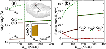
Figure 26. (a) Thermal evolution of lattice parameters of a ferroelectric SnSe monolayer as a function of an effective temperature  . (b) Evolution of lattice constants. The evolution is calculated using a normalised Boltzmann distribution over the energy landscape. Reprinted (figure) with permission from [26]. Copyright (2022) by the American Physical Society.
Download figure:
Standard image High-resolution imageThermal averages of elastic constants Cij are then determined by [260]
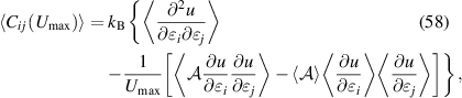
(with  Boltzmann's constant,
  , and
, and  ) and presented in figure 26(b).
At energies above  the 2D material transitions from a rectangular onto a square unit cell and
  and
and  must be identical, but that is not obtained when employing the regular expression for strain based on a zero-temperature value (equation (55)). The need for
  for
for  dictates the redefinition of equilibrium lattice parameters evolving with temperature (equation (56)), and hence of a thermally-evolving strain.
 is the softest elastic modulus and
  hardens at the transition (
 ), while
  softens at
  . According to figure 26(b), SnSe monolayers are softer than graphene, for which
  N m−1, and
  N m−1.
By direct comparison J and TC
from numerical calculations [239], a correspondence  is established, such that
  K, and finite−T elastic behaviour can be extracted from figure 26(b).
3.6.6. Photostriction: anisotropic, non-thermal strain created by illumination.
The discussion now turns into optical ways to modify lattice parameters in a non-thermal manner, but with illumination.
Illumination by light can excite electrons onto the conduction band, changing the electronic density away from its ground state configuration. The modification of the electronic density–in turn–screens the intrinsic electric dipoles of 2D ferroelectrics, producing uniform and anisotropic strain as a result. The process, called photostriction, was theoretically predicted on group-IV monochalcogenide (SnS, SnSe, and GeS) monolayers [7].
The atomistic structure of a SnS monolayer is shown in figure 27(a), and its electronic band structure in figure 27(b). The material has an indirect bandgap, with the top of the valence band at the valley dubbed nX (which stands for near X-point) and the bottom of the conduction band at the valley labelled nY (for near Y-point).

Figure 27. (a) Structural snapshot of a SnS monolayer. The four atoms in the unit cell are indicated. The direction of the intrinsic electric dipole are shown by red arrows in the top view, and the side view features a 0.3 eÅ‒3 isosurface. (b) Three direct optical transitions between valence and conduction bands. (c) Monolayer states at the nX conduction local valley minima have mostly px
orbital symmetry. (d) Reduction of the magnitude of the intrinsic electric dipole P as a result of photoexcitation to occupy the states in the nX conduction valley indicated within inset. (e) The longer lattice parameter a1 elongates and the shorter lattice parameter  shrinks as a result of the photoexcitation. Reprinted (figure) with permission from [7]. Copyright (2017) by the American Physical Society.
Download figure:
Standard image High-resolution imageIndirect optical transitions require momentum transfer and have low probability of occurrence. For this reason, one considers direct optical transitions instead. Three such transitions are indicated by arrows on figure 27(b). The local valence band valleys at the nX, Γ, and nY k-points have a predominantly s-orbital (spherically-symmetric) hybridisation, and the largest change in intrinsic polarisation occurs upon transitions onto px and py orbitals. The electronic wavefunction densities at the conduction band edges at the nX k-point is shown in figure 27(c) [7].
Working on a  k-point grid and considering spin–orbit coupling, one gets a density of charge carriers
  , where A0 is the area of the unit cell before the photoexcitation. Setting
  , a photoexcitation around the nX
k-point is simulated by sequentially changing of occupation of the valence band edge by the removal of the occupation at points labelled 1, 2, and 3 within the inset in figure 27(d), promoting the removed electronic density into the conduction band at the same k-point(s), and relaxing the structure. This way, the intrinsic polarisation is shown to decrease as a result of the photoexcitation, which screens P (see its decreasing value in figure 27(d)). Furthermore, while the unit cell remains rectangular with lattice parameters
, a photoexcitation around the nX
k-point is simulated by sequentially changing of occupation of the valence band edge by the removal of the occupation at points labelled 1, 2, and 3 within the inset in figure 27(d), promoting the removed electronic density into the conduction band at the same k-point(s), and relaxing the structure. This way, the intrinsic polarisation is shown to decrease as a result of the photoexcitation, which screens P (see its decreasing value in figure 27(d)). Furthermore, while the unit cell remains rectangular with lattice parameters  , one observes in figure 27(e) that a2 increases in magnitude while a1 decreases. This way, one achieves an optomechanical coupling to produce anisotropic strain by illuminating 2D ferroelectrics. The realisation of photostriction in 2D materials is important because the photostriction response time depends on the sample's thickness, ranging from picoseconds in thin films up to a few seconds in the bulk [7].
The effect described in figures 27(d) and (e) persists upon a reflection of the structure depicted in figure 27(a) with respect to the yz plane; an operation that swaps the direction of the intrinsic electric dipole from the  onto the
  direction. Then, photostriction is not limited to monolayers, but it persists in bulk layered (orthorhombic) IV–VI compounds with an antipolar dipole configuration [246]. Briefly breaking the logical flow of the update to discuss experiments carried out on a bulk sample now, a technique called megaelectronVolt ultrafast electron diffraction was employed to confirm an expansion of a2 and a contraction of a1 on bulk (layered) GeS [8]: measured strains of 0.1% are consistent with those predicted in [7]. Furthermore, and as seen in figure 28, they also report an ultrafast photoexcitation of the order of 10 picoseconds.
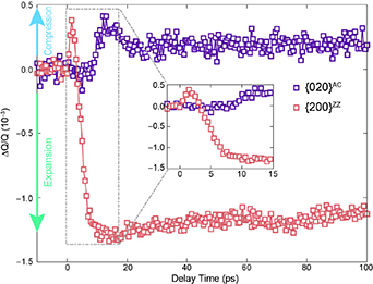
Figure 28. Experimental demonstration of photostriction on orthorhombic, bulk GeS. The sample was excited by a 400 nm femtosecond laser with a photon energy above GeS' bandgap and probed by ∼100 fs ultrashort electron pulses at normal incidence. The reversible photoinduced mechanical deformation of the lattice was obtained from the shift of Bragg peak center positions in reciprocal space (Q). The  (
( ) direction corresponds to the x (y) direction in figure 27(a). As seen in figure 27(e), an anisotropic strain in which the x direction compresses and the y direction elongates is experimentally verified. Reprinted with permission from [8]. Copyright (2023) American Chemical Society.
Download figure:
Standard image High-resolution image3.6.7. Using uniaxial strain to tune the critical temperature of 2D ferroelectrics.
Similar to graphene, it may be possible to strain 2D ferroelectrics by clamping them onto a substrate and a subsequent bending (figure 29(a)) and one wonders how strain affects the critical temperature Tc at which the intrinsic electric dipole turns zero. To determine the effect of strain on Tc , multiple structural order parameters such as angles and interatomic distances of a ferroelectric SnSe monolayer were tracked as a function of temperature (figure 29(b)) through ab initio molecular dynamics calculations.
Figure 29. (a) Ferroelectric SnSe monolayer clamped onto a strained substrate. (b) Clamping prevents  from becoming zero (panel (i)), which is no longer a good order parameter to tell the structural transformation. Nevertheless, a 2D structural phase transition can still be registered if angles α1 and α3 turn identical (panel (ii)), and distances d2 and d3 turn equal as well (panel (iii)). (c) Thermal evolution of (i) lattice parameters a1 and a2, (ii)
  , (iii) angles α1, α2, α3, and α4, (iv) distances d2 and d3, and in-plane intrinsic dipole (
 ) under a 2% strain along the x-direction (the 2D material is still able to change a2, which is not fixed). As a result of strain, Tc
increased up to 500 K. (d) Similar to (c), but for a strain applied along the y-direction: strain raises Tc
to 250 K.
) under a 2% strain along the x-direction (the 2D material is still able to change a2, which is not fixed). As a result of strain, Tc
increased up to 500 K. (d) Similar to (c), but for a strain applied along the y-direction: strain raises Tc
to 250 K.  increases regardless of the clamping direction, and it can swap the intrinsic electric dipole from being oriented along the x-direction (plot (c)) onto the y-direction (plot (d)). Solid curves in plots (c) and (d) are the result of a Potts model. Reprinted (figure) with permission from [238]. Copyright (2018) by the American Physical Society.
Download figure:
Standard image High-resolution imageThe results are presented in figure 29(c) for strain applied along the x-direction, and in figure 29(d) when strain is applied vertically. Datapoints are results from molecular dynamics, and solid lines (when present) correspond to a Potts model [238, 261]. The extreme right within the yellow boxes to the left of figures 29(d) is the value of Tc without applied strain.
As seen in figure 29(c), a modest strain of 2% along the direction defined by the largest lattice vector a1 increases the value of  –from about 2∘ in the non-clamped SnSe monolayer (figure 24(c)-(iii))–up to about 3.3∘; see subplot (ii) in figure 29(c).
Still considering subplot (ii) in figure 29(c), one sees that clamping precludes a situation in which  . In this case, and as illustrated in figure 29(b), a transition from a rectangular onto another rectangular unit cell takes place though. In those rectangular cells, the transition takes place through the coalescence of angles α1 and α3, and of distances d2 and d3. Tc
increases regardless of the direction in which uniaxial tensile strain is applied. (Symbols
. In this case, and as illustrated in figure 29(b), a transition from a rectangular onto another rectangular unit cell takes place though. In those rectangular cells, the transition takes place through the coalescence of angles α1 and α3, and of distances d2 and d3. Tc
increases regardless of the direction in which uniaxial tensile strain is applied. (Symbols  stand for thermal averages.)
There are few studies addressing the electronic properties of group-IV monochalcogenide monolayers at domain walls [25, 245, 248, 262], and the amount of strain at those appears to be rather small.
3.6.8. 2D bismuth: an elemental ferroelectric monolayer.
The attention now turns to two atomic layers of bismuth, in which a new frontier in 2D elemental ferroelectrics is arising [263]. (On a bilayer configuration, this material couples a non-trivial electronic topology with ferroelectric behaviour [264].) Similar to SnTe, bulk bismuth has a rhombic structure in the bulk [265, 266]. In the recent past, a structural transformation on ultrathin SnTe was determined whereby it turns into a (layered) orthorhombic phase instead [267, 268].
Consisting of a single chemical element, if a similar rhombic to orthorhombic transition is to take place in bismuth (whose electronic configuration is 6s26p3), one may first imagine that its 2D structural configuration may resemble that of phosphorene (electronic configuration 3s23p3), a non-ferroelectric 2D material possessing a center of inversion [251–253].
Nevertheless, and as stated in [263], the larger principal number on bismuth–and its disposition within the Periodic table of the Elements in between insulators and metals–makes its electronic configuration different from that of phosphorus, to the point of developing a net in-plane intrinsic dipole  : while the 3s and 3p orbitals lie at comparable energies in phosphorene, the 6s orbitals lie at a significantly lower energy than the 6p orbitals, which weakens their sp : unlike phosphorene, in which bonds are shared s and
  orbitals, atomic bonding on Bi monolayers is mainly due to
  orbitals. Furthermore, the originally degenerate pz
orbitals split by occupying the lowermost and highermost atoms within the bilayer, in an electronic configuration resembling that of group-IV monochalcogenide monolayers whereby the chalcogen is more negatively charged: this intrinsic electronic redistribution (polarisation) creates two sublattices and drives the intrinsic electric dipole with an in-plane polarisation in bismuth monolayers.
orbitals. Furthermore, the originally degenerate pz
orbitals split by occupying the lowermost and highermost atoms within the bilayer, in an electronic configuration resembling that of group-IV monochalcogenide monolayers whereby the chalcogen is more negatively charged: this intrinsic electronic redistribution (polarisation) creates two sublattices and drives the intrinsic electric dipole with an in-plane polarisation in bismuth monolayers.
The atomistic configuration of the bismuth monolayer in figure 30(a) thus resembles that seen in group-IV monochalcogenide monolayers [246] (figures 24(c)-(ii), 27(a), and 29(b)). Unlike phosphorene–similar to the structure B in figure 30(b)—it features different heights for all four atoms in the unit cell, and a twice-degenerate energy landscape reminiscent of that of figure 24(c)-(i) that is depicted in figure 30(c).
Figure 30. As, Sb, and Bi monolayers undergo a structural distortion onto a ferroelectric phase with an in-plane intrinsic electric polarisation P. (a) Generic atomistic structure. (b) Ferroelectric phases (A and A') and a rectangular paraelectric phase (B) with a higher symmetry. (c) Two-fold degenerate elastic energy landscape as a function of the height of the red atoms in (b); blue atoms were left unchanged with respect to their positions in structure B. (d) An electronic reconfiguration of pz orbitals onto outermost atoms drives the creation of a purely-electronic in-plane intrinsic dipole P. Figure taken from [263]. John Wiley & Sons. © 2018 WILEY-VCH Verlag GmbH & Co. KGaA, Weinheim.
Download figure:
Standard image High-resolution imageEven though there are four bismuth atoms in the unit cell, the two ones closest to vacuum receive extra charge from pz orbitals, giving the unit cell two nonequivalent atoms and a Pmn21 space group, just like that taking place in group-IV monochalcogenide monolayers [246].
Structure A' (B) here was labelled B in figure 24(c)-(i). Structure B here is calculated on the same rectangular unit cell used to compute structures A and A', while structure C in figure 24(c)-(i) was calculated on the minimal-energy square unit cell and are thus not equivalent. The charge distribution underpinning the electronically-driven intrinsic dipole is displayed in figure 30(d).
Similar to the experimental realisation of SnTe monolayers [248], bismuth monolayers were also grown in epitaxial graphene. The authors verified its in-plane intrinsic electric polarisation by noticing that the higher-most atom appears bright (dark) in valence (conduction) band sweeps [257], thus confirming the non-equivalence of bismuth atoms in the unit cell.
Furthermore, polarisation switching by the field created by the tip was observed at a domain wall, which verifies the ferroelectric character of 2D bismuth experimentally.
Unlike the case of the SnTe monolayer [262, 267], and similar to SnSe monolayers on epitaxial graphene [245], the bismuth monolayer displays 180∘ domain walls [257].
3.7. Tuning the magnetic configuration of 2D magnets by strain
Strain can modify the spin configuration of magnetic 2D materials and make them undergo ferromagnetic (FM) to antiferromagnetic (AFM) phase transitions [269–271].
As a first example–obtained via Monte Carlo calculations–uniaxial compressive strain was applied to CrGeTe3 monolayers to switch in between FM and AFM phases. The switching of magnetic phases happens by crossing a region of parameter space with a high degree of magnetic frustration (f) [269]. Uniaxial strain breaks the equivalency Cr−Cr bonds and modifies exchange coupling parameters, resulting in a change in magnetic configuration [269].
A zero-temperature, quantum phase transition from a FM to an AFM takes place at about 2.8% uniaxial compressive strain applied along the zigzag direction. The critical temperature increases for larger compresive strain (figure 31(a)). On the other hand, FM and AFM phases are separated by 2.9% compressive strain at zero temperature when strain is applied along the armchair direction (figure 31(b)) [269].

Figure 31. (a) Magnetic phase diagram versus percent strain and temperature for a CrGeTe3 monolayer under uniaxial compressive strain along the zigzag ( ) direction. (b) Similar to (a), but for compressive strain along the armchair (
 ) direction. The color coding corresponds to the level of magnetic frustration (f). Insets depict the AFM phases, with black and white circles representing Cr ions with opposite spin directions. Reprinted (figure) with permission from [269]. Copyright (2021) by the American Physical Society.
Download figure:
Standard image High-resolution imageSimilar strain-induced magnetic phase transitions have been predicted for CrI3, CrSe2, and CrTe2 [270, 271].
3.8. Magnetoelectric multiferroic monolayers
This section is written to highlight a new frontier on 2D materials that is quickly converging with another area of research dealing with bulk materials having combined magnetic and electric ferroic orders. This section will also serve as preamble for a discussion of engineered multiferroics on magnetic bilayers.
NiI2 is a layered material with a screw spin helix in an otherwise centrosymmetric lattice [272]. As it turns out, the electromagnetic coupling takes place within a generalised Katsura–Nagaosa–Balatsky interaction that is written as follows [273]:

where  is the intrinsic electric polarisation vector (at point i in the lattice, created by a spin at lattice positions i and i), M is the electromagnetic coupling, Si
is the spin at location i, and Sj
the corresponding spin at location j. Such polar helimagnetic phase persists down to a monolayer, making NiI2 the first experimentally-verified 2D multiferroic hosting an improper electronic ferroelectricity, where P is driven by an inversion-symmetry-breaking screw spin helix, in an otherwise centrosymmetric lattice. Spin interactions beyond nearest-neighbour Ni sites stabilise the screw spin helix.
is the intrinsic electric polarisation vector (at point i in the lattice, created by a spin at lattice positions i and i), M is the electromagnetic coupling, Si
is the spin at location i, and Sj
the corresponding spin at location j. Such polar helimagnetic phase persists down to a monolayer, making NiI2 the first experimentally-verified 2D multiferroic hosting an improper electronic ferroelectricity, where P is driven by an inversion-symmetry-breaking screw spin helix, in an otherwise centrosymmetric lattice. Spin interactions beyond nearest-neighbour Ni sites stabilise the screw spin helix.
The discussion of monolayers ends at this point, to give way to a discussion of novel phenomena taking place in few-layer materials.
4. Strained multilayers (including moirés)
The emphasis turns into stacks of 2D materials in what follows. We start with a discussion of non-rotated bilayers and few-layers, and end with a discussion of few-layers with relative rotations (moirés).
4.1. Energy landscape of slid homo-bilayers without relative rotations
Homo-bilayers are created out of monolayers made from the same 2D material. A hetero-bilayer, on the other hand, is made from two dissimilar 2D materials and it will always produce a moiré. The discussion in the rest of this review is mostly on homo-bilayers and on stacks made from the same 2D material. Hetero-layers will only be discussed when dealing with encapsulated devices here.
To understand the atomistic reconstructions taking place in moirés, it is illustrative to first realise that there is an optimal stacking of two monolayers on a homo-bilayer without relative rotations. The optimal stacking can be calculated using ab initio techniques that yield (sliding) energy landscapes similar to those displayed in figures 24(subplots (i)) and 30(c) (later on, figure 43(a) will feature an energy landscape as well).
Indicated in figure 32(a), graphene's preferred bilayer stacking is labeled AB [275] (or BA) and it is two-fold degenerate. Binary compounds expand the number of possible stacking sequences, and a hBN bilayer can be either set on its lowermost energy configuration AA' (figure 32(b)), or on the AB configuration seen in figure 32(c) (which is related by a 60∘ rotation–or a reflection of the upper monolayer in the AA' structure given the three-fold symmetry).
Figure 32. (a) Three possible stacking sequences of a graphene bilayer; the AB stacking is the preferred one. (b) Three stacking sequences for a hexagonal boron nitride bilayer. The AA' staking is the preferred one. (c) Reflecting the upper hBN bilayer, additional stacking sequences without a center of inversion arise. Similar stacking sequences to subplots (b) and (c) can be set on TMDC bilayers. Reprinted (figure) with permission from [274]. Copyright (2015) by the American Physical Society.
Download figure:
Standard image High-resolution imageThe energy landscapes on figures 33(a), (c), (e), (g) and (h) indicate the optimal relative placement of a homo-bilayer without moiré. The important observation is the existence of two degenerate energy minima per unit cell in figures 33(a), (e) and (h). Those minima correspond to the structures shown in figures 34(a), (b), (c), (d) and (f). The (degenerate) energy landscapes can be fitted to the following function [274]:
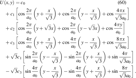
All bilayers with a honeycomb lattice have sliding energy landscapes like the ones shown in figure 33 [274, 276].

Figure 33. (a) Energy landscape of a graphene bilayer; the AB stacking is the preferred one, and it is degenerate (note the dark blue regions). On the other hand, the AA-stacked configurations (shown in red) are the most energetically unfavorable. (b) Corresponding optimal relative height of the graphene bilayer. (c) Optimal energy and (d) relative height of the hexagonal boron nitride bilayer, originally on the AA' configuration (darkest blue). (e) Energy landscape and optimal relative height of the non-centro-symmetric hexagonal boron nitride bilayer: note the existence of degenerate two minima within the unit cell. Reprinted (figure) with permission from [274]. Copyright (2015) by the American Physical Society. (g) Energy landscape of a WSe2 2H bilayer; it has only one minima in the unit cell. (h) Energy landscape of the non-centro-symmetric rhombic WSe2 bilayer. Reprinted with permission from [276]. Copyright (2022) American Chemical Society.
Download figure:
Standard image High-resolution image
Figure 34. (a) AB bilayer graphene [275]. (b) BA bilayer graphene can be obtained by a reflection or by a relative sliding (see degenerate minima in figure 33(a). (c) Substitution of carbon atoms in the AB configuration by boron and nitrogen removes the point of inversion, creating an intrinsic electric dipole P that (d) switches direction upon reflection and/or sliding (see figure 33(e) for the two degenerate minima within the unit cell). Adapted with permission from [277]. Copyright (2017) American Chemical Society. This phenomenology extends to other readily available bilayers, such as TMDC (MX2) bilayers, which have a center of inversion in their 'hexagonal' (H) conformation, but lack a point of inversion in their 'rhombohedral' (R) configuration, and develop an out-of-plane intrinsic electric dipole P as well. Reprinted with permission from [278]. Copyright (2018) American Chemical Society.
Download figure:
Standard image High-resolution imageWhile the discussion of ferroelectric monolayers was taking shape (see section 3.6.3 and [246]), Li and Wu determined a way to generalise 2D ferroelectrics into more widely available and chemically inert bilayers of 2D materials such as hBN [277] and TMDCs [278] by removing their center of inversion through a relative 60∘ rotation among monolayers. Such insightful realisation led to an increased interest in ferroelectricity at the two-dimensional limit that remains ongoing.
4.2. Paraelectric behaviour of homo-bilayers by 'telegraph-noise' shear sliding
Recent experimental work showed a transition from a ferroelectric configuration on WSe2 bilayers (one in which the intrinsic electric dipole moment P is finite) onto a paraelectric one (in which P = 0) at finite temperature [279]. The atomistic phenomena leading to a paraelectric behaviour on those homo-bilayers is quite different to that observed in ferroelectrics before, where a two-fold degenerate energy landscape (figure 35(a)) suffices to describe such behaviour.

Figure 35. (a) Ferroelectrics are traditionally described by a polynomial energy landscape with two degenerate minima, an energy barrier J, and energy-confining potential energy walls. (b) Rhombohedrally-stacked (R) TMDC bilayers are unusual ferroelectrics having an infinite number of degenerate minima. The paraelectric state is the time average of P over long times; P swaps sign at random times and it averages down to zero. (c)–(f) Demonstrating the temperature-activated relative sliding of the R WSe2 bilayer: The vector  tracks a pair of W atoms belonging to opposite monolayers on the same unit cell as a function of time. Sliding events are observed at temperatures above 490 K; the magnitude of those displacements is consistent with the vectors drawn as an inset in plot (c) which furnish a honeycomb lattice. The critical temperature TC
is assigned to that for which the first sliding event occurs within the full 1 µs simulation time. Reprinted with permission from [276]. Copyright (2022) American Chemical Society.
tracks a pair of W atoms belonging to opposite monolayers on the same unit cell as a function of time. Sliding events are observed at temperatures above 490 K; the magnitude of those displacements is consistent with the vectors drawn as an inset in plot (c) which furnish a honeycomb lattice. The critical temperature TC
is assigned to that for which the first sliding event occurs within the full 1 µs simulation time. Reprinted with permission from [276]. Copyright (2022) American Chemical Society.
Download figure:
Standard image High-resolution imageThe first observation to justify a novel description of ferroelectricity on bilayers lacking a center of inversion is the presence of multiple degenerate minima (two per unit cell) that are all accessible by sliding (figure 35(b)).
The second observation is that the paraelectric phase is created by sliding events on the honeycomb lattice, with the out-of-plane polarisation P changing direction at every discrete sliding step shown in figures 35(d)–(f) [276].
A third and most remarkable experimental observation is that layered ferroelectrics can sustain an intrinsic electric polarisation that increases in discrete steps with the number of added monolayers [280].
As it turns out, it is extremely challenging to realise bilayers with lattice vectors of each monolayer forming exact multiple of 30∘ angles with respect to one another [281]. This fact will give rise to a wealth of physical behaviours that will be surveyed in the next section.
4.3. Moiré patterns
4.3.1. Relevance and brief historical survey.
The word moiré has an arabic origin and it means 'to wet.' The term is commonly used within the textile industry to describe the appearance of interwoven silk and it should not be capitalised.
The first observation of moirés on turbostatic graphite dates back to 1993 [282]. (This moiré has been revisited quite recently [283].) According to [284], the first observation of unusual electronic properties on rotated bilayer graphene moirés is due to Eva Andrei [285], who determined that the energy separation between van Hove singularities reduces with the relative angle of rotation among monolayers, and posited that their energy separation would be zero at an angle smaller than 1.1∘ (a magic angle), at which point the linear momentum of charge carriers would turn zero as well. Calculations of a rotated graphene bilayer performed within a continuum model demonstrated the possibility of renormalisation of the Fermi velocity of graphene [286]; velocity renormalisation was confirmed by tight-binding calculations [287, 288]. Bistritzer and MacDonald suggested the possibility of strongly correlated electron–electron quantum phases at the flat bands taking place at magic angles [289]. The subsequent experimental confirmation of unconventional superconductivity and correlated insulating phases by Jarillo-Herrero's group [290] has led to intense and ongoing research in this area. Nowadays it is known that velocity renormalisation also takes place in other moiré 2D materials, such as a twisted hBN bilayer [291]. The experimental challenges in creating precise rotations have been addressed in a recent review [281].
4.3.2. Different ways to create moirés.
There are multiple ways to create moirés [292] with 2D materials out of the following basic 'ingredients:'
- (i)by a relative twist between two monolayers in a homobilayer
- (ii)by isotropically straining one monolayer in a homobilayer
- (iii)by relative shear strain in a homobilayer
- (iv)by uniaxial simple shear in a homobilayer
- (v)by an unrelaxed hetero-bilayer
- (vi)by stacking more than two monolayers with angular stacking faults
The first three of those alternatives are shown in figure 36.

Figure 36. Strain from (a) twisting, (b) isotropic strain, or (c) pure shear have signatures that allow identification from one another. Reproduced from [292], with permission from Springer Nature.
Download figure:
Standard image High-resolution imageThe rotated homo-bilayer moiré is the most commonly described in the theoretical literature, and the process to create a commensurable moiré bilayer by a relative rotation is described now. When commensuration between the two monolayers exists, the lattice vectors of a rotated moiré supercell can be obtained following a process delineated in [282, 292–295] and multiple other publications. Let
be a matrix built from the lattice vectors written down in equation (1). (Lattice vectors were written in column form in equation (61).)
Let θ be the mismatch angle (this is, the relative rotation angle between the two monolayers). Customarily, the lower monolayer is rotated by  , while the upper monolayer is rotated by
  . The respective rotation matrices are:
and the moiré superlattice vectors (figure 37(a)) are obtained as:
where


Figure 37. (a) Wigner–Seitz supercell of a twisted graphene moiré bilayer (atomic positions were not relaxed). Regions with AA, AB and BA stacking configurations, as well as the moiré lattice vectors a1 and a2 are indicated. (b) Reciprocal lattice of the twisted bilayer graphene. High-symmetry points are indicated along with moiré reciprocal lattice vectors  and a set of vectors
  . (a) Reprinted (figure) with permission from [296]. Copyright (2021) by the American Physical Society. (a) Reprinted (figure) with permission from [297]. Copyright (2022) by the American Physical Society.
Download figure:
Standard image High-resolution imageare the rotated lattice vectors for the lower and upper monolayer, respectively. Carrying out the math, the moiré lattice vectors (equation (62)) are given by:
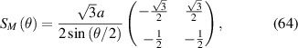
or

with the length of the moiré superlattice vector given by 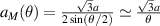 for
for  (when expressed in radians). The area of the moiré is given by
 ![$\mathrm{Area}_M(\theta) = [\frac{\sqrt{3}}{2}a_M(\theta)]^2\simeq \frac{3a^2}{2}\theta^{-2}$](https://content.cld.iop.org/journals/0034-4885/87/1/016502/revision2/ropad06dbieqn286.gif) , and the corresponding reciprocal space is shown in figure 37(b).
, and the corresponding reciprocal space is shown in figure 37(b).
Strain and corrugations play a major role in the TBG flat band and energy gaps at the magic angle [298]. As seen in figures 36(a)–(c), different sections of the bilayer form relative conformations that explore every local unit cell configuration seen in figure 33. In principle, the energy cost varies, and certain configurations can be minimised by a process of local atomistic (strain) reconstruction [17, 283, 299–304]; Cazeaux et al have deployed a process to optimise moiré bilayers that minimises a functional of the local strain [292]. It relies on an energy landscape set on a unit cell similar to the one given by equation (60) (but slightly simpler). Configurations (a)–(c) in figure 36 lead to triangular homo-bilayer moirés and to experimentally differentiable patterns.
The energetic preference for AB and BA regions over AA stacking regions (see figure 37(a)) leads to lattice deformations and local strain [17, 19, 292, 298, 305] due to the steric repulsion between carbon pz
orbitals. Therefore, carbon atoms move apart from each other producing a corrugation that tracks the different kinds of stacking regions. As seen in figure 38, DFT calculations indicate that out-of-plane displacements are accompanied along with significant in-plane relaxation [19]. A vortex-like pattern can be observed in figure 38. The direction of circulation on the vortex reverts in between monolayers. Overall, the atomic relaxation results in the shrinking of the AA stacking regions in favor of the  stacking domains [19].
Figure 38. TBG in plane relaxation for (a) the top and (b) bottom graphene layers for a mismatch angle of  . The vectors represent the displacement field. Its magnitude is also highlighted by colour. Perfect AA stacking points are at the corners. The minimally strained regions are AA stacking-like. Vortices of the strain field are seen around AA like regions. One dimensional channels are also seen. Reproduced from [19]. CC BY 4.0.
Download figure:
Standard image High-resolution imageAt very small twist angles ( ), the structural relaxation in TBG leads to the formation of triangular domains with Bernal stacking. Under an interlayer bias, these domains are gapped and the electronic transport occurs in one-dimensional networks formed by domain walls. Those states have been visualised in experiments recently [17, 299]. Transport in these one-dimensional networks has been studied using a model where the AA regions in TBG are represented as scattering centers connected by one-dimensional helical channels [306, 307]. Pseudo Landau levels and an effective honeycomb lattice for this model were also discussed [308].
The structural relaxation of AA stacking regions diminishes the tunneling in such regions. Theoretically such tunnelling can be set to zero resulting in a chiral model that contains the basic features of the magic angle physics [296, 297, 309, 310]. In fact, it can be proved that the squared chiral Hamiltonian is basically a Quantum Hall effect hamiltonian [310]. From the chiral model, one can obtain the magic angles for multilayer graphene [311].
The consequences of strain in the interacting phase diagram of TBG were investigated recently [312]: even for small strain ε (within the range of values observed in experiments), strain-induced topological phase transitions occur, supporting the possibility of strain playing an important role in sample-dependent observations. Along those lines, the role played by strain in the fabrication of moiré materials has been recently studied from a reproducibility perspective [281]. The presence of non-uniform strain in TBG might lead to variability in transport results within different regions of a single TBG sample. Models to determine twist angle and strain have been developed [313–315].
Small strains at nonzero integer fillings have been predicted to stabilise an 'incommensurate Kekulé spiral' order [316] (section 3.2.7).
In a study using an atomistic description of TBG [317], the role of a hBN substrate in the structural relaxation and band structure of TBG was shown to be important, introducing large effective masses and large pseudo-magnetic fields. Also, the long-range Coulomb electron–electron interaction affects the distribution of Berry curvature of the bands near charge neutrality of a TBG closely aligned with hBN. Due to the suppressed dispersion of the narrow bands, the band structure is strongly renormalised [54]. Therefore, the topological linear and nonlinear Hall conductivities in TBG/hBN are substantially modified by electron–electron interactions [54].
4.3.3. Real-space topology and strain on moiré bilayers.
Figures 39(a)-(i–iv) contain possible relative displacements of the upper monolayer (in orange) with respect to the lower (blue) one. Those displacements, when folded back onto the unit cell, define an order parameter [315].

Figure 39. (a) Subplots (i)–(iv): definition of possible atomic displacements; the direction of relative monolayer motion is coded by color. Subplot (v) folds the displacements back into a single unit cell, and it defines an order parameter. (b) Transmission electron microscopy and Fourier transforms permit identifying the type of moiré created. For instance, the domains seen in subplots (i)–(v) correspond to a moiré created away from a bilayer near an AB configuration, while those in subplots (iv) and (vi) take place in a moiré near an AA' configuration. (c) Identification of domains and domain walls (see figure 36). (d) Probability of displacements folded into a single unit cell: coloring is consistent with that in subplot (c). Reprinted (figure) with permission from [315]. Copyright (2023) by the American Physical Society.
Download figure:
Standard image High-resolution image'First order' domain walls obtained by dark field transmission electron microscopy are displayed in figure 39(b)-(i), while 'second order' images (which focus on the domain walls) can be seen in figures 39(b)-(ii–iv). The colors displayed on figures 39(b)-(ii–iii) are consistent with those displayed in figure 36. Figure 39(c) contains domain structures and domain walls. Note how the AA regions have collapsed onto smaller areas; the AA configurations correspond to the points in which two boundary lines in the unit cell in figure 39(d), which are avoided due to their high energy cost (see (red) maxima of the energy landscape at AA onfigurations in figure 33).
The topology of the unit cell can be equivalently observed in the unit cell (figures 39(a)(v), 39(d), and 40(a)) or in the torus displayed as figure 40(b). The crucial point is that the AA regions, being so energetically costly, collapse onto sections with a negligible area, and are explicitly removed ('cut out') in the topological description. Another equivalent description of the topology is obtained by joining the three (green, blue, and red) lines into points AB and BA, as it is done in figure 40(c) [315].
Figure 40. (a) The order parameter observed in figure 39(d) can be redrawn (b) as a cut torus that avoids configuration AA, or (c) as three lines joining two points AB and BA. (d) A loop round a configuration AA, which is thus avoided. (e)–(h) Real-space dislocations corresponding to clockwise paths in configuration space, generating vortices ((e) and (f)) and antivortices ((g) and (h)). Domain walls were coloured based on the R, G, or B move in configuration space. The direction of the moves is shown by black arrows. The structures were created from: (e) isotropic, (f) twist, (g) uniaxial, and (h) shear displacements. Reprinted (figure) with permission from [315]. Copyright (2023) by the American Physical Society.
Download figure:
Standard image High-resolution imageTo understand the topology of the relative displacements, figure 40(d) depicts a hexagonal circuit, whose center is an (avoided) AA configuration. The direction of a given displacement can be further encoded by the addition of 'inverse' operations, which reverse direction. This way, one works with those elements:

An additional simplification calls for the following redefinition of group elements:

the definition of operations in terms of group generators a and b permits defining a vortex operation:

which, starting at a configuration BA, goes clockwise (from left to right; figure 40(d)). An antivortex operation goes anticlockwise on figure 40 [315]:

Figure 41 combines analyses of topology and geometry of a WSe2/MoSe2 moiré hetero-bilayer.

Figure 41. (a) Dark-field TEM image of a WSe2/MoSe2 hetero-bilayer. The scale bar is 100 nm. The inset contains a diffraction pattern and Burgers vectors. (b) Vortex density. (c) Isotropic strain map. (d) Uniaxial strain map. (e) The shear strain has magnitudes around 1% in highly elongated domains. (f) Twist is the largest contributor to the moiré. Reprinted (figure) with permission from [315]. Copyright (2023) by the American Physical Society.
Download figure:
Standard image High-resolution image4.3.4. Magic angle twisted bilayer graphene.
A powerful method to describe the structure of twisted 2D materials relies on the cut and projection method used to generate quasicrystals [294, 318–320]. There, the projected structure is interpreted as the set of points of best fit between the two rotated structures [294].
A paradigmatic model for the electronic properties of TBG is described by a  matrix operator. The starting point is the Bistritzer–MacDonald Hamiltonian [289], obtained by rotating two graphene low-energy effective Dirac Hamiltonians [1], and coupling the two graphene monolayers using the first harmonics of the interlayer interaction potential only [289, 321].
Considering as a basis set the wave vectors  , where the index 1 or 2 labels a graphene monolayer and
  and
and  are the two Wannier orbitals on each inequivalent site (sublattice) of the graphene's unit cell [1], the chiral Hamiltonian is given by [309, 311]:
Zero-mode operators are defined as:
and
where  is the antiholonomic differential operator and
  the holonomic one. The dimensionless coupling (potential) is given by:

where  and the moiré reciprocal lattice vectors are given by
  ,
,  ,
,  (see figure 37(b)).
The moiré modulation vector is
where θ is the twist angle between layers and  is the Dirac wave vector norm. The angle and interlayer coupling effects are both captured by the parameter α, defined as:
with  meV the interlayer coupling for AB stacking and
  is the Fermi velocity.
The spectrum can be found by proposing a Bloch wave function with momentum k in the moiré first Brillouin zone:
and
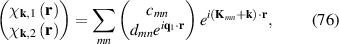
and solving for the coefficients  ,
,  ,
,  , and
, and  in the Hamiltonian (69).
Figure 42 presents the resulting squared energies E2 as a function of α obtained at three k-points: Γ-, K, and  , the last one being a k-point of low symmetry. Working with E2 instead of E helps emphasise the magnitude of the energy–given that the spectrum is electron–hole symmetric. The band edge is located at the
  point and the dips in figure 42 correspond to the magic angles
  , because the band shrinks to zero width for those values of the twist angle θ (see equations (73) and (74)).

Figure 42. Numerically found lowest-band logarithm of the squared energy of the twisted bilayer graphene versus the parameter α (related to θ): The upper red dots corresponds to the Γ point; black dots to the  point, while purple dots correspond to another generic k point, i.e. chosen no to be a high symmetry point, in this case
  . At magic α's, indicated by vertical red lines, the bandwidth goes to zero, as indicated by a drop in the band energy values. The K point is always a zero solution for any α. Reprinted (figure) with permission from [297]. Copyright (2022) by the American Physical Society.
Download figure:
Standard image High-resolution imageChiral symmetry induces an electron–hole symmetry [322–325] that leads into an effective  Hamiltonian. Squaring
  , it decouples into two identical
  matrices given by [296]:
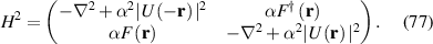
The squared norm of  can be understood as an effective confinement potential in the moiré supercell:
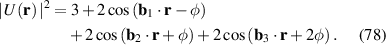
As seen in figure 43(a),  resembles a Kagome lattice.
The off-diagonal terms of the  matrix are:
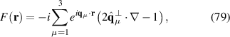
and,
where  with
with  and
and  . This is an essential point as eigenvalues must be real (notice that
  ).
).  is a set of unitary vectors perpendicular to the set
  such that
  .
.
The contributions from  and
and  can be condensed into a new operator
proportional to an interlayer current between different bipartite lattices [297] and, eventually, with the angular momentum in the perpendicular direction to the two graphene monolayers: for small twist angles, the squared TBG chiral model Hamiltonian turns out to be akin to a Quantum Hall effect Hamiltonian [310, 326].
The renormalisation simplifies the Hamiltonian considerably and highlights the three main ingredients of charge carrier dynamics on twisted few-layers: (i) a kinetic energy contribution via the  term, (ii) a confinement, kind of quantum dot, potential energy
  , and (iii) the interaction operator
  , which is an interlayer current between bipartite lattices that eventually results in a coupling of angular momentum and an effective magnetic field [326].
The expectation values from those three energy terms are presented as a function of the (twist-angle dependent) parameter α at the Γ point in figure 43(b). The kinetic and confinement potential contributions are always positive while the angular contribution is always negative. The first magic angle is different from others, but reachable through perturbation theory [297]. As seen in figure 43(c), the flat band can be understood as a very special condition in which the sum of kinetic and confinement energy is equal to the angular effective confinement contribution achieved through destructive interference paths [310]. Another interesting feature can be seen in figure 43(c): the magic angles follow a quantised rule  , where m is the order of the twist angle
  [310]. The wave functions at magic angles are nearly coherent Landau levels and thus have many important properties and applications [310].
The renormalisation produced by the squaring procedure maps the flat band into a ground state separated by a gap from the rest of the states. The ground state has an antibonding nature in a triangular lattice and then has frustration, associated with a massive degeneration [98, 296, 322–324]. Also, this renormalisation is equivalent to a supersymmetric transformation from a fermion to a bosonic Hamiltonian, a subject of intense research in solid state physics [327, 328].
An intriguing and yet unexplored feature is the equivalence of the flat band with floppy modes on elastic Hamiltonians [296] for mechanical systems with constraints, such as rods or bars between hinges [329–331], or glasses [332, 333].
The chirality of TBG seems to induce spin textures around the K point of the Brillouin zone with alternating vortex-like textures [334]. The helicity of each vortex is inverted by changing the chirality. The spin texture changes as the twist angle evolves.
A unified picture of the quantum phase diagram of TBG in terms of incommensurate Kekulé spiral (IKS) order was proposed recently [316, 335]: this is a time-reversal-symmetric and spatially nonuniform order, which shifts the spatial coordinates and rotates the U(1) angle characterising the spontaneous intervalley coherency simultaneously [316]. Also, many different flavors of fermions can be obtained by making heterostructures of Kekulé over another Kekulé-patterned graphene [336].
Intercalating graphene layers with alkali atoms leads to effects similar to strain [337]. Although those results seem to be relevant for the alkali-intercalated systems where Kekulé patterings have been reported [158, 176], the relation between intercalation and strain has not been discussed in the literature to the best of our knowledge.
Measurements of the second order transversal conductivity have been used to detect topological transitions in strained moiré systems [338], as the latter are closely related to the changes in sign of the Berry dipole. In strained TBG, it has been observed that the nonlinear effects can be even more important than the linear ones [339]. Similar nonlinear effects have been seen in rotated bilayers of WSe2 [340], where a change in the sign of the Berry dipole across the gap has been identified. The effect is enhanced due to the large spin–orbit gap typical of TMDCs [341]. Apart from charge transport, thermal and thermoelectrical transport have also been investigated in strained TBG [342].
4.3.5. Antiferroelectric moiré bilayers.
At the 2D limit, the electric field effect can penetrate a bilayer, and ferroelectric metals exist in WTe2 bilayers [343]. Here, one continues the discussion started in section 4.1 concerning ferroelectric insulating bilayers though. More specifically, figures 34(c) and (d) indicate that the (insulating) hBN bilayer switches its direction of polarisation P as it changes from the AB to the BA configuration. This means that, when a a moiré structure is set with a small angle δ away from the configurations drawn in figures 33(e), (g) and (h), a domain structure like the one shown in figure 42(a) will set up. Additionally, if the types of strain shown in figures 42(b) and (c) are also taking place, those will also give rise to an antiferroelectric disposition that is experimentally depicted by piezo-force microscopy in figure 44. The effect has been experimentally generalised to moiré TMDC bilayers as well [283, 300–302]. That the intrinsic polarisation P increases in discrete steps with additional layers has been demonstrated as well [280].

Figure 43. (a) Dimensionless confinement potential  for a twisted bilayer graphene model in which the tunnelling at AA regions is set to zero. The degenerate minima of
  occurs at AA (green dot) and AB (red dots) stacking points. The maximum are located at BA stacking points (yellow dots). The Wigner–Seitz cell of the moiré lattice is indicated (see figure 37(a)). (b) Expectation values of the components of H2 at the Γ point, as a function of α near the first magic angle (vertical line). Numerical results are indicated with dashed lines and points.
  is shown in blue,
  is green. The off-diagonal contribution
  is seen in black and orange, corresponding to the first and second terms in equation (79). The solid lines are analytical, perturbative solutions [297]. (c) Kinetic plus confinement energy expectation value without the absolute value of the angular momentum contribution at the Γ point. Flat-bands arise at magic angles (vertical lines) whenever the kinetic, confinement and angular momenta contributions add up to zero. The kinetic and confinement potential contributions are positive, while the angular contribution is negative. Reprinted (figure) with permission from [297]. Copyright (2022) by the American Physical Society.
Download figure:
Standard image High-resolution image
Figure 44. (a) Small-angle twisted hexagonal boron nitride bilayer. The red circled dot and red circled X represent up and down polarisation, respectively. (b), (c) Vertical piezo-force microscopy phase and amplitude images. From [300]. Reprinted with permission from AAAS.
Download figure:
Standard image High-resolution image4.3.6. Flat bands, charge localisation, and electronic correlations in non-graphene moiré homo-bilayers.
Flat bands and strong electronic correlations are not exclusive of magic-angle moiré graphene bilayers. As seen in figure 45, charge localisation extends to multiple moiré homo-bilayers such as the hBN one [291, 344–346]. Strong electron–electron correlations on flat-band non-graphene bilayers are being vigorously studied now [347].
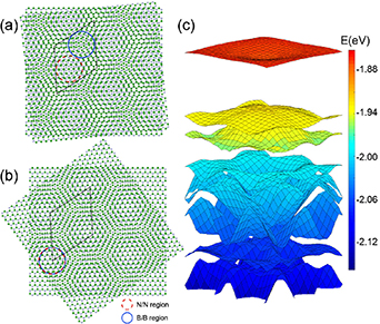
Figure 45. (a) Hexagonal boron nitride bilayer with a small moire away from configuration BN/BN-2 in figure 32(c). (b) Hexagonal boron nitride bilayer with a small moire away from configuration BN/BN-1 (lower in energy) in figure 32(b). (c) Flat band on a moiré hexagonal boron nitride bilayer with a rotation angle of 2.64∘ away from the BN/BN-2 configuration. Reproduced from [291]. CC BY 4.0.
Download figure:
Standard image High-resolution image4.4. An argument for charge localisation in graphene and hexagonal boron nitride moiré homo-bilayers
The domain walls separating AB and BA regions develop a limit length [292]. At that limit, electronic states belonging to AB and BA domains happen to be orthogonal. This is proven for a graphene bilayer, and it can be proven for a hBN bilayer along similar lines.
To prove the orthogonality of electronic states belonging to either and AB or a BA domains in bilayer graphene, the π-electron Hamiltonian in [275] will be employed. In the absence of external out-of-plane electric field or dopants, it reads as:
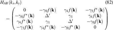
with  the usual factor introduced in [1],
  eV,
eV,  eV,
eV,  eV,
eV,  eV, and
  eV [275, 348].
The π-orbitals used to build the Hamiltonian in equation (82) are ordered as A1, B1, A2, and B2, where the letter A or B indicates the sublattice within a given layer, and the subindex (1 or 2) indicates the layer to which a given orbital belongs.
Starting from an AB bilayer, the Hamiltonian for a BA bilayer requires an inversion along the z-direction (see figures 34(a) and (b)), or a monolayer relabeling leading to:
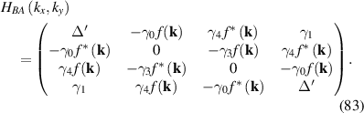
Focusing on the energy dispersion at the Dirac points, the question is whether an electronic state at zero energy at a AB domain at one K-point can be transmitted onto the BA domain at the same K-point. This question is addressed by looking at whether the relevant states are orthogonal: if they were, states at the AB domain cannot be transmitted onto a BA domain.
For definiteness, the K-point oriented along the +x direction will be considered for this argument. Such K-point will be labelled  .
.  at any of the K-points, so equation (82) simplifies into:

Permuting columns on equation (84) the following way:

leads to the Hamiltonian
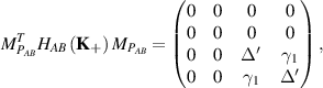
with eigenvalues  , 0 (double degenerate), and
  . The associated eigenvectors, written in the original orbital order (
 ) are:
On the other hand, equation (83) simplifies into
which, under the following column permutation
also leads to

with identical eigenvalues to those of  :
:  , 0 (doubly degenerate), and
  , and associated eigenvectors, written in the original orbital order (
 ):
):
Then, all energy states turn out to be orthogonal at AB and BA domains; this is especially true for the zero-energy states, which belong in orthogonal subspaces:
The argument provided in this subsection can help explain the gradual process toward velocity renormalisation in moiré graphene and hBN homo-bilayers. The localisation of charge due to orthogonality of charge carriers at AB and BA domains then underpins the strong electron–electron interactions taking place in those rotated bilayers.
4.5. Correlated physics in triple-layer graphene
More recently, triple layer twisted graphene has been found to be the most strongly interacting correlated material [349, 350], and quasi-crystalline electronic phases have been uncovered on those systems [351]. Given that they share similar quantum phase diagrams, such discoveries unveiled the possibility of using 2D materials to understand unconventional superconductivity in cuprates and heavy fermion systems [290, 312, 349, 352, 353].
The search for superconductivity and other correlated phases in graphene-based materials was extended to non-twisted graphene multilayers. Remarkably, superconductivity was reported in ABC (or rhombohedral) trilayer graphene [354] and Bernal-stacked blayer graphene.
For one of the superconducting phases found in ABC-trilayer graphene, multiple studies have focused on a purely electronic mechanism [355]. A proposal by Ghazaryan et al [356] pointed out a general mechanism for superconductivity induced by an annular Fermi surface. Remarkably, an annular Fermi surface has not only been observed in ABC-trilayer graphene, but in other graphene superlattices [154] as well.
4.6. Modified optical properties of transition metal dichalcogenide monolayers by strain
Single-photon emitters from 2D materials provide unique advantages over existing quantum light sources and may have potential applications in quantum cryptography and quantum computing. Recently, a van der Waals heterostructure consisting of a WSe2 monolayer, hBN, and few-layer graphene (FLG) was fabricated to produce electric field-tunable single photon emission [29] by optical excitation. As seen in figure 46, demonstrations of electrical excitation of photoemitters on strain-tunable van der Waals heterostructures have been provided as well [357].

Figure 46. (a) Vertical heterostructure (top graphene/WSe2 monolayer/h-BN/bottom graphene on a polymer substrate). The optical emission site is located below the AFM tip. (b) Band bending of the strained heterostructure under an external bias. EB
, EV
, ED
, and  are the excitonic bright band, valence band, dark excitonic band, and defect state of the WSe2 monolayer. Solid and dashed red lines in the right panel are spatial variations of the band gap due to local strain. (c) Fabrication process: (i) A PMMA layer was spin-coated on top of the TMDC on the SiO2/Si substrate, and peeled off. (ii) The detached PMMA layer was turned upside down. (iii) AFM indentation was performed afterwards. (d) Optical microscope image of the heterostructure. Scale bar: 10 µm. (e) AFM image of the fabricated heterostructure. Seven indents were made to the WSe2 monolayer. Scale bar: 5 µm. Reproduced with permission from [357]. CC BY-NC 4.0.
Download figure:
Standard image High-resolution imageBy applying an electric field, the electron and hole wave functions become spatially separated, resulting in a change in the total energy of the trapped exciton. Electric field-tuned SPE can be observed at positions where strain is induced by a nanopillar. These strain-induced emitters have higher emission energies (blueshifts) than previously reported quantum emitters in WSe2 monolayers [29, 358].
4.7. Ferroelectric non-centrosymmetric few-layer elemental stacks
In connection with section 3.6.8, elemental, non-centrosymmetric four-layer graphite has been shown to turn ferroelectric theoretically (figure 47) [359, 360] and experimentally [361]. Polar and non-polar configurations can be reached by the relative sliding of specific monolayers within the stack. Besides it being yet another example of elemental ferroelectricity, this recent finding of polar behaviour on few-layer graphite is quite relevant from a historic perspective.

Figure 47. Triangular domains in marginally-twisted tetralayer graphene (2AB+2BA, 3ABA+1 and 3ABC+1). Domains with and without ferroelectric behaviour are shown on the right and left sides of the figure. Reproduced from [359]. CC BY 4.0.
Download figure:
Standard image High-resolution imageIndeed, there was a strong focus on ways to open a gap in the early days of graphene research (this in order to create transistors out of graphene). One way to do so involves placing a graphene bilayer under an external electric field [275, 362, 363]. The ability to create an intrinsic or internal electric field in tetralayer graphene results in the creation of a (small) band gap.
4.8. Tuning magnetism on few-layer magnets by tensile uniaxial strain
Strain has been put forward as a way to control the magnetic properties of thin layered materials. To give an example, a strain-induced antiferromagnetic-to-ferromagnetic phase transition was realised on ∼20 nm thick CrSBr flakes; magnetoelastic couplings can give rise to skirmion patterns [364].
4.9. Engineered bilayer multiferroics by rotations and shear strain
Creating intrinsic electric dipoles can also be combined with magnetism, providing a novel method for magnetoelectric multiferroics in rotated 2D materials.
Antiferromagnetically (AFM) oupled CrI3 bilayers are one of the most studied magnetoelectric multiferroic 2D materials [365–368]. Electric control of magnetism on AFM-coupled CrI3 bilayers was demonstrated through second harmonic generation [369].
By rotating the upper monolayer by 60∘, the centre of inversion of the CrI3 AB configuration is removed, resulting in an intrinsic electric dipole. A rotated bilayer (labelled s1 in figure 48) belongs to the crystalline space group Cm. The upper layer of the bilayer s1 can be further displaced by approximately 2a1/3 (labelled s ) or 2a2/3 (labelled s
 ), resulting degenerate structures (s
 and s
and s ) that still belongs to the same crystalline space group, Cm. As a result, it creates an out-of-plane electric dipole moment and an even stronger in-plane intrinsic electric dipole.

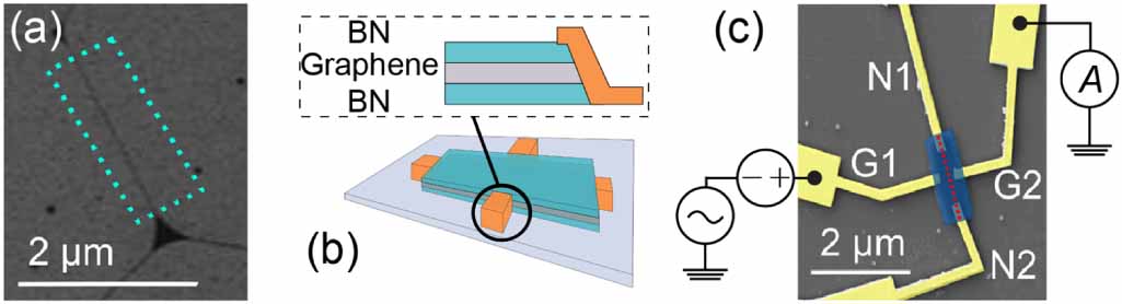
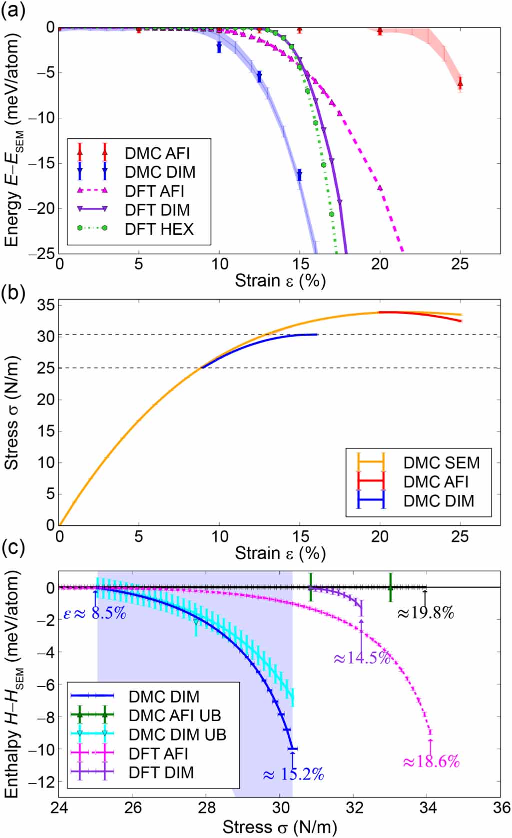
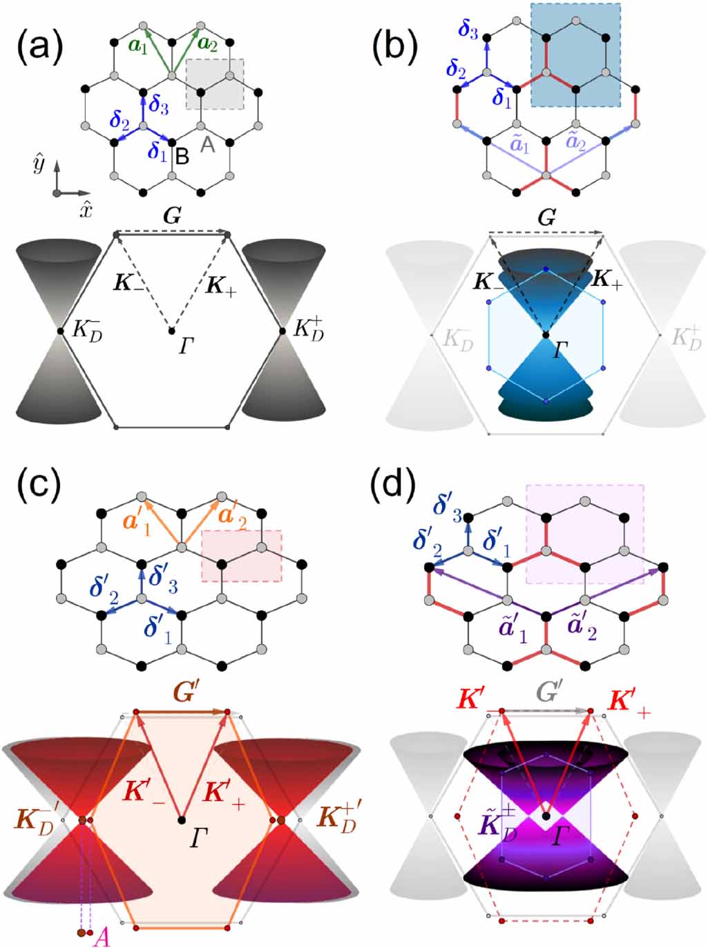
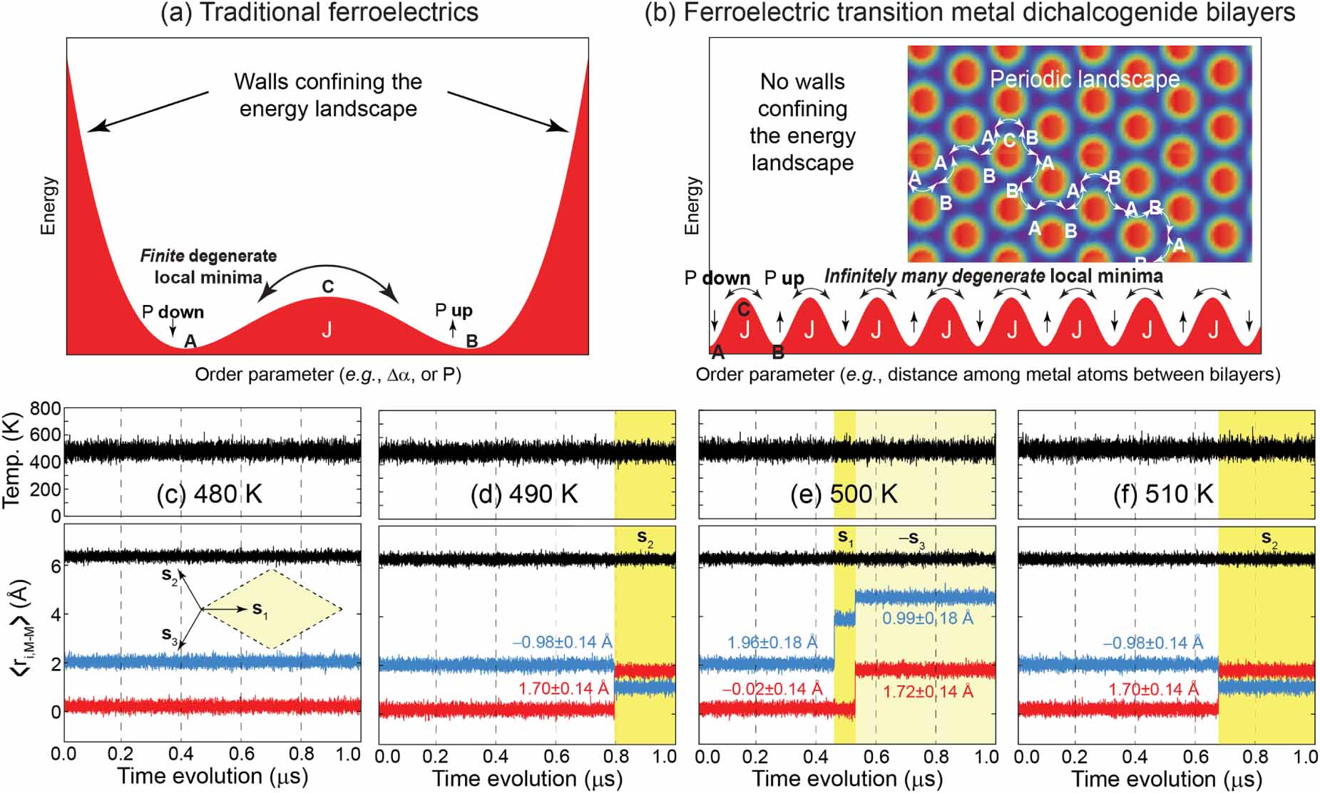
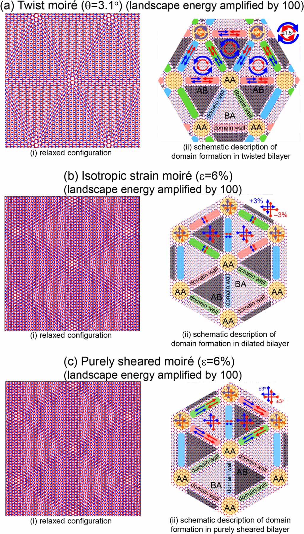
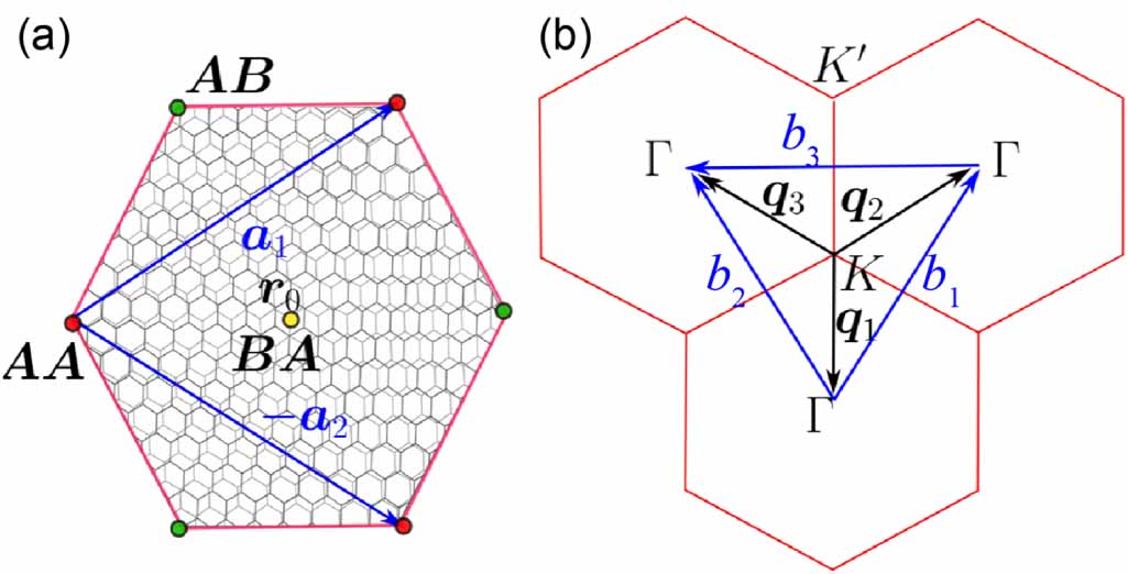
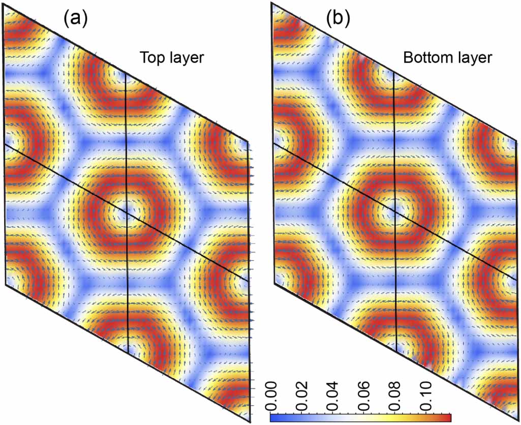
Figure 48. (a) Energy landscape of CrI3 bilayer with FM (uuuu) and AFM (uudd) magnetic configurations, and optimal vertical separation between monolayers (D). Structure s1 sits at the point from which lattice vectors a1 and a2 join, and it is periodic upon lattice translations. Structure s (s
(s ) sits 0.6389a1 (0.6806a2) away from s1 locations. (b) One-dimensional cuts of the energy landscape along (i) a1 and (ii) a2. (c) Structural stability of s1 bilayer, and vibrations at saddle point p, displaying imaginary modes. (d) Three-dimensional electric dipole along the straight path joining structures s1 and s
 . Inset: change in magnetisation at a nearly degenerate crossover AFM and FM configurations at point p (see inset labeled `along a1' in subplot (b)). Reprinted (figure) with permission from [370]. Copyright (2023) by the American Physical Society.
Download figure:
Standard image High-resolution image
The coupling of electric and magnetic moments leads to a novel magnetoelectric coupling, as follows [371]:
in Gaussian units [370].
5. Conclusion
It may be fair to say that a natural state of atomistic membranes is one of local strain. Here, experimental and theoretical avenues to strain graphene and other metallic, insulating, ferroelectric, ferroelastic, ferromagnetic and multiferroic 2D materials were reviewed. A broad emphasis was placed on:
- valley and sublattice polarisation (P) in graphene
- time-dependent strain on graphene
- local and/or global strain and superconductivity and other highly correlated and/or topological phases of graphene
- piezoelectric P hBN monolayers
- strain and the optoelectronic properties of TMDCs
- ferroic 2D materials with intrinsic elastic (σ), electric (P) and magnetic (M) polarisation under strain, as well as incipient 2D multiferroics
- moiré few-layers exhibiting flat electronic bands and exotic quantum phase diagrams, and other bilayer or few-layer systems exhibiting ferroic orders tunable by rotations and shear strain.
Realisations of a tunable two-dimensional Quantum Spin Hall effect in germanene, of elemental 2D ferroelectric bismuth, and 2D multiferroic NiI2 were highlighted as well.
The comprehensive discussion of effects of strain facilitated within this Update can be seen as an integral and necessary component for the holistic understanding of 2D materials. The authors hope that the breadth and the number of extremely recent works reviewed help jumpstart research avenues for a broad range of researchers on this burgeoning field.
Acknowledgment
G G N thanks UNAM-DGAPA Project IN101924 and CONACyT Project 1564464. S A H acknowledges CONACyT, México for a PhD Scholarship. S B L was funded by the U.S. Department of Energy (Award DE-SC0022120). H N acknowledges support from the MonArk NSF Quantum Foundry supported by the National Science Foundation Q-AMASE-i program under NSF Award No. DMR-1906383 and the Department of Defense under award FA9550-23-1-0500. We thank E Andrade-Amezcua, R Carrillo-Bastos, L Navarro, P Pantaleon, F Guinea, J Roll, J Ferrer, A Garcia-Fuente, A Pacheco-Sanjuan, P Kumar, M Asmar, A Huamán, S Patel, A Singh, and A Ceferino for scientific discussions, help with figures, or for their critical reading of the manuscript.
Data availability statement
Data for figure 22 can be provided by H N upon request. No other new data were created or analysed in this study.