


Abstract
Wide bandgap aluminum gallium nitride (AlGaN) semiconductor alloys have established themselves as the key materials for building ultraviolet (UV) optoelectronic and power electronic devices. However, further improvements to device performance are lagging, largely due to the difficulties in precisely controlling carrier behavior, both carrier generation and carrier transport, within AlGaN-based devices. Fortunately, it has been discovered that instead of using AlGaN layers with fixed Al compositions, by grading the Al composition along the growth direction, it is possible to (1) generate high-density electrons and holes via polarization-induced doping; (2) manipulate carrier transport behavior via energy band modulation, also known as 'band engineering'. Consequently, such compositionally graded AlGaN alloys have attracted extensive interest as promising building blocks for efficient AlGaN-based UV light emitters and power electronic devices. In this review, we focus on the unique physical properties of graded AlGaN alloys and highlight the key roles that such graded structures play in device exploration. Firstly, we elaborate on the underlying mechanisms of efficient carrier generation and transport manipulation enabled by graded AlGaN alloys. Thereafter, we comprehensively summarize and discuss the recent progress in UV light emitters and power electronic devices incorporating graded AlGaN structures. Finally, we outline the prospects associated with the implementation of graded AlGaN alloys in the pursuit of high-performance optoelectronic and power electronic devices.
Export citation and abstract BibTeX RIS
1. Introduction
The III-nitride family (AlN, GaN, InN, and their alloys) has been regarded as one of the most significant semiconductors, and has therefore been heavily investigated in the past two decades for both optoelectronics [1–5], and power electronics applications [6–9]. In the field of optoelectronics, remarkable achievements in the crystal growth, material doping, and device fabrication of InGaN-based light emitters have revolutionized the lighting industry, promoting energy-efficient and eco-friendly modern solid-state lighting and lasing technologies [4, 10–13]. Similarly, by alloying GaN with AlN, we can synthesize Alx Ga1−x N (0 ⩽ x ⩽ 1) ternary alloys with tunable direct bandgaps from 3.4 eV (GaN) to 6.1 eV (AlN) by simply varying their alloy compositions, corresponding to a wide UV spectral range from 360 nm to 210 nm, for a broad range of applications including air/water purification, UV curing, data storage, optical communication, etc. [14–16]. Hence, AlGaN alloys have attracted enormous attention in the nitride community for use in efficient AlGaN-based UV optoelectronic devices [1–3, 14]. In the field of power electronics, AlGaN alloys possess superb material properties including large critical electric fields, high electron mobility, and an excellent power figure of merit [6, 9, 17], making them very suitable for developing power electronic devices which operate in sophisticated electronic systems such as power grids, wireless communications, space exploration, and radars, which require higher frequencies and higher power capacities than existing technologies based on other semiconductors such as silicon (Si) and gallium arsenide (GaAs) [6, 7, 17–19].
Although AlGaN-based UV optoelectronic and power electronic devices have shown tremendous potential due to their excellent optical and electrical features, several crucial issues have impeded their further development for widespread application. On one hand, insufficient carrier generation due to conventional impurity doping, especially hole doping, in Al-rich AlGaN materials hinders the realization of highly conductive p-AlGaN films for sufficient current injection [20]. Moreover, the typical designs of multiple quantum wells (MQWs) and p-type electron barrier layers (p-EBLs) in conventional AlGaN UV light emitters normally lead to poor electron confinement capability and limited hole injection efficiency, which greatly affect the radiative recombination efficiency [21]. As a result, the power conversion efficiency of AlGaN-based UV light emitters drops to single digits (less than 10%) in comparison with their counterpart InGaN-based blue light emitters (which achieve more than 80%), [13] particularly when the emitted wavelength becomes shorter than 280 nm [1]. On the other hand, the mainstream study of AlGaN-based power electronic devices is moving towards higher-frequency and higher-powered applications [6, 9, 17–19, 22, 23]. However, under such conditions, the behavior of electrons generally suffers from severe problems such as reduced electron mobility in the conductive channels and increased electron leakage into the buffer layers [24–28]. Besides, to enhance the breakdown voltage (BV), Al-rich AlGaN channels have become popular for high-voltage and high-frequency applications [6, 7, 29]. However, the poor electron concentration in such channels, together with the increased electron barrier height at the source and drain contacts, result in both high series and contact resistance. Consequently, the current density and power density of Al-rich AlGaN-based transistors are severely suppressed [7, 29].
In view of the drawbacks that exist in AlGaN-based devices, better control of carrier generation and transport, which are the fundamental carrier behaviors in the abovementioned devices, are urgently needed. Intriguingly, it has been discovered that AlGaN alloys with a graded Al composition can offer an effective approach for manipulating carrier behavior. Figure 1 illustrates the specific roles that graded AlGaN alloys can play in the operation of optoelectronic and power electronic devices. On the one hand, graded AlGaN alloys can naturally produce three-dimensional electron or hole carriers via polarization-induced doping [20]. As a result, such conductive layers have been utilized as either the n- or p-type current injection layers in UV light emitters [30–37] or as the conductive channels in AlGaN transistors [38–45]. On the other hand, it was discovered that by bridging different layers via a graded AlGaN structure, it is possible to effectively manipulate the carrier transport behavior within devices by either raising or lowering the energy-band structures, i.e. by so-called 'band engineering'. For example, studies have demonstrated that graded-AlGaN-based quantum wells (QWs), quantum barriers (QBs), and p-EBLs can improve carrier confinement in active regions without hindering hole injection, thus boosting the internal quantum efficiency (IQE) and light output power (LOP) of UV light emitters [21]. As for power devices, graded AlGaN structures can act as back-barrier layers beneath the conductive channels, so that electrons can be sufficiently confined [27]. Furthermore, an ohmic contact layer in the form of a graded AlGaN structure can be inserted on top of the AlGaN barrier layer to reduce the electron barrier height at the source and drain contacts [46–51].
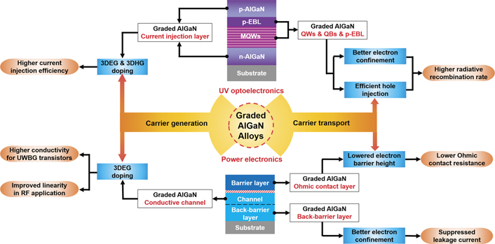
Figure 1. Summary of the key roles of graded AlGaN alloys in manipulating carrier behavior, including carrier generation control via polarization-induced doping and carrier transport control via band engineering in both UV optoelectronic and power electronic devices.
Download figure:
Standard image High-resolution imageIn essence, the effective carrier behavior manipulation enabled by compositionally graded AlGaN alloys can greatly enhance the performance of AlGaN-based UV optoelectronic and power electronic devices. It is the aim of this review to elaborate on the physical and material properties of graded AlGaN alloys and present a summary of the explorations of their use in both optoelectronic and power electronic devices, highlighting device design and an analysis of the underlying device operation mechanisms. In section 2, the physics behind the use of graded AlGaN alloys for effective carrier behavior manipulation are comprehensively discussed. In sections 3 and 4, UV light emitters and power electronic devices employing graded AlGaN structures are separately reviewed, focusing on the promotion of device performance enabled by higher carrier generation due to polarization-induced doping and better carrier transport manipulation via band engineering. Finally, we present conclusions and perspectives on the further implementation of graded AlGaN alloys, shedding light on the development of future efficient optoelectronic and power electronic devices.
2. Controlling carrier behavior in graded AlGaN alloys
2.1. Carrier generation via polarization-induced doping
As members of the III-nitride family, AlGaN alloys crystallized in the wurtzite (WZ) structure are most thermodynamically stable at room temperature at standard atmospheric pressure, and have therefore been investigated the most for device applications [52]. In a WZ AlGaN structure, Ga/Al and N atoms are tetrahedrally bonded with each other, and based on the different stacking sequences of the atomic layers, metal-polar (Ga/Al-polar) and N-polar AlGaN alloys are separately defined, as shown in figures 2(a) and (b). In a single tetrahedron, there is a large electronegative difference between neighboring Ga/Al and N atoms. Therefore, each bond can be treated as a microscopic electric dipole P 0. Since WZ AlGaN alloys deviate from an ideal centrosymmetric tetrahedron along the c-axis, the vector sum of four electric dipoles in an AlGaN tetrahedron leads to non-neutralized components Δ P along the [000-1] orientation, as annotated in figures 2(a) and (b). Besides, the WZ structures lack inversion symmetry centers, so the residual Δ P can accumulate along the c-axis and generate macroscopic polarization fields, known as spontaneous polarization (denoted by P sp ). Furthermore, when AlGaN thin films are under external stress, two types of homogenous in-plane strain, i.e., tensile strain and compressive strain, are produced. Accordingly, additional net polarization fields Δ P add are generated in the c-axis direction, as annotated in figures 2(c) and (d). This net polarization, derived from external stress, is known as piezoelectric polarization (denoted by P pz ).

Figure 2. (a), (b) Schematically illustrate the formation of spontaneous polarization (Psp) in the [000-1] direction in Al-polar and N-polar WZ AlGaN alloys, respectively. Lattice deformation and piezoelectric polarization (Ppz) formation in Al-polar AlGaN alloys under (c) tensile strain and (d) compressive strain are also illustrated.
Download figure:
Standard image High-resolution imageTwo types of polarization effect, including spontaneous and piezoelectric polarization, are significant properties of AlGaN alloys. One of the most successful uses of such effects is the production of a polarization-induced two-dimensional electron gas (2DEG) in GaN-based heterojunction field-effect transistors (HFETs), also known as high electron mobility transistors (HEMTs) [17–19]. Figure 3(a1) shows a schematic of an Al-polar AlGaN/GaN HFET. Because of polarization effects, equivalent polarization charge distributions are exhibited in the HFET in figure 3(a2), where σsp and σpz stand for the sheet charge densities generated by spontaneous polarization and piezoelectric polarization, respectively. Due to the discontinuity of polarization fields across the heterostructure, net-positive sheet polarization charges (σpol) are formed at the AlGaN/GaN heterointerface; the charge density can be calculated by σpol = ( ) −
) −  [53]. Those polarization charges can further induce electrons ionized from the surroundings such as remote dopants and surface states, and therefore produce 2DEGs as dense as ∼1013 cm−2 at the heterointerface without incorporating any intentional impurity dopants [54–56]. Besides, strong polarization fields can largely bend the band structure of the AlGaN/GaN HFET, forming a narrow and deep conductive channel at the interface to confine the polarization-induced 2DEG, as illustrated in figure 3(a3). Similarly, HFETs based on a GaN/AlGaN heterostructure, as shown in figure 3(b1), can generate a two-dimensional hole gas (2DHG) at the heterointerface. Figures 3(b2) and (b3) are the separate corresponding equivalent polarization charge distribution and band diagrams of a GaN/AlGaN HFET. Recently, Chaudhuri et al successfully demonstrated a polarization-induced 2DHG in an undoped GaN/AlN heterostructure with a high density of 5 × 1013 cm−2 [57], providing an alternative p-type doping strategy for AlGaN-based optoelectronic and power electronic devices.

Figure 3. Schematic illustrations of polarization-induced 2DEG and 2DHG in Al-polar AlGaN-based heterojunctions. In (a1) AlGaN/GaN and (b1) GaN/AlGaN heterojunctions, (a2) positive and (b2) negative polarization charges are spontaneously generated at the heterointerfaces, respectively. As a result, (a3) 2DEG and (b3) 2DHG are polarization induced at the narrow QWs bent by the strong polarization electric fields.
Download figure:
Standard image High-resolution imageFurthermore, instead of forming abrupt AlGaN/GaN heterojunctions, we can spread out the fixed polarization charges at the heterointerfaces in a three-dimensional way by steadily increasing or decreasing the Al composition in AlGaN alloys along the growth direction. The charge profiles are determined by the divergence of polarization fields, as given by  , where
  is the charge density along the growth direction z, and P is the total polarization field of the graded AlGaN alloy [58, 59]. Consequently, mobile three-dimensional electron and hole carriers are generated by those unbalanced polarization charges; importantly, this type of carrier concentration and profile can easily be modulated by specially designing the grading scheme of AlGaN alloys [38, 58, 59].
A polarization-induced three-dimensional electron slab, also referred to as a three-dimensional electron gas (3DEG), in graded AlGaN alloys was first verified by Jena and Mishra et al in the early 2000s [58, 59]. They achieved a 1018 cm−3 3DEG concentration in an AlGaN alloy that was linearly graded from GaN to Alx
Ga1−x
N in the [0001] growth direction, as shown in figure 4(a1) [58]. Unbalanced positive polarization charges were generated in the whole graded structure (figure 4(a2)), which were able to attract a mass of electrons from the surroundings to form a 3DEG in the graded AlGaN alloy, as illustrated in figure 4(a3). This type of linear grading profile leads to an approximately uniform doping profile ![$\rho \left(z\right)=\left[{P}_{A{l}_{x}G{a}_{1-x}N}-{P}_{\text{GaN}}\right]/t$](https://content.cld.iop.org/journals/0034-4885/84/4/044401/revision3/ropabde93ieqn5.gif) , where
, where  is the total polarization of the Alx
Ga1−x
N surface and t is the thickness of the graded AlGaN layer. Correspondingly, the band diagram and 3DEG carrier profile in graded AlGaN alloys with an increased Al composition along the growth direction are plotted in figure 4(a4). So far, the carrier concentration of a polarization-induced 3DEG has been able to reach an order of 1020 cm−3 following structural optimizations [60]. Similarly, Zhang et al confirmed that a 3DHG could also be induced by polarization by linearly decreasing the Al composition in the [0001] direction, as shown in figure 4(b1) [61]. The corresponding charge distribution, polarization-induced 3DHG, and band diagram with the carrier profile of such graded AlGaN structures are plotted in figures 4(b2)–(b4), respectively. The observed hole concentration in the graded AlGaN alloys (from Al0.3Ga0.7N to GaN) reached a level of ∼1018 cm−3 [61]. Subsequently, Li et al demonstrated 3DHGs in Al-rich graded AlGaN alloys (from AlN to Al0.7Ga0.3N) with a hole concentration of 1018 cm−3, showing great potential for realizing highly conductive Al-rich AlGaN films [62].
is the total polarization of the Alx
Ga1−x
N surface and t is the thickness of the graded AlGaN layer. Correspondingly, the band diagram and 3DEG carrier profile in graded AlGaN alloys with an increased Al composition along the growth direction are plotted in figure 4(a4). So far, the carrier concentration of a polarization-induced 3DEG has been able to reach an order of 1020 cm−3 following structural optimizations [60]. Similarly, Zhang et al confirmed that a 3DHG could also be induced by polarization by linearly decreasing the Al composition in the [0001] direction, as shown in figure 4(b1) [61]. The corresponding charge distribution, polarization-induced 3DHG, and band diagram with the carrier profile of such graded AlGaN structures are plotted in figures 4(b2)–(b4), respectively. The observed hole concentration in the graded AlGaN alloys (from Al0.3Ga0.7N to GaN) reached a level of ∼1018 cm−3 [61]. Subsequently, Li et al demonstrated 3DHGs in Al-rich graded AlGaN alloys (from AlN to Al0.7Ga0.3N) with a hole concentration of 1018 cm−3, showing great potential for realizing highly conductive Al-rich AlGaN films [62].
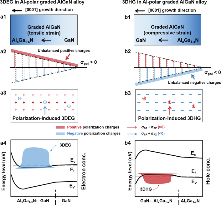
Figure 4. (a1) Schematic view of Al-polar AlGaN alloy with an increasing Al composition along the growth direction. Positive unbalanced charges (a2) and the formation of a polarization-induced 3DEG (a3) are also illustrated. The corresponding band diagram and 3DEG carrier profile are plotted in (a4). Similarly, (b1)–(b4) show Al-polar AlGaN alloy with a decreasing Al composition along the growth direction, its unbalanced positive charge distribution, its 3DHG formation, and a band diagram with the hole carrier profile, respectively.
Download figure:
Standard image High-resolution imageIntriguingly, it is noted that the generative mechanism of 3DEG and 3DHG strongly depends on the polarity of the AlGaN films. By simply flipping the polarity of AlGaN structures, Simon et al successfully demonstrated polarization-induced 3DHG in N-polar graded AlGaN alloys, as illustrated in figures 5(a1)–(a4) [30]. They further incorporated such graded alloys into UV light-emitting diodes (UV LEDs) as a highly conductive p-type current injection layer. The device exhibited a six-fold higher hole concentration and a roughly thirty-fold enhancement in electroluminescent (EL) intensity, compared with non-graded AlGaN-based UV LEDs. A 3DEG can also be generated in an N-polar downward-graded AlGaN alloy (from Alx Ga1−x N to a GaN surface), as illustrated in figures 5(b1)–(b4). In particular, N-polar GaN/AlGaN heterostructures have attracted widespread attention for device applications. In comparison to Al-polar AlGaN/GaN heterojunctions, the N-polar GaN/AlGaN structure possesses lower Al composition and barrier height at the semiconductor's surface, which is beneficial in reducing the contact resistance of AlGaN UV light emitters and power electronic devices [45, 63–65]. More importantly, researchers have further confirmed that the carrier densities of 3DEG and 3DHG are nearly temperature-independent, since those carriers are mostly polarization-induced. On the contrary, the carrier concentration of conventional Si-doped n-AlGaN and Mg-doped p-AlGaN alloys decreases exponentially at low temperatures, due to the freeze-out effect of thermally activated electrons and holes [30, 63].

Figure 5. (a1) Schematic view of N-polar AlGaN alloy with an increasing Al composition along the growth direction. Negative unbalanced charges (a2) and the formation of a polarization-induced 3DHG (a3) are also illustrated. The corresponding band diagram and 3DHG carrier profile are plotted in (a4). Similarly, (b1)–(b4) show N-polar AlGaN alloy with a decreasing Al composition along the growth direction, its unbalanced negative charge distribution, its 3DEG formation, and a band diagram with the electron carrier profile, respectively.
Download figure:
Standard image High-resolution image2.2. Manipulation of carrier transport via energy band engineering
The previous section elaborated how carriers can be generated via graded AlGaN alloys. In this section, we focus on how such alloys can control and affect carrier transport behavior. In general, the aims of carrier transport manipulation in AlGaN optoelectronic and power electronic devices can be categorized as: (1) to achieve efficient carrier migration and injection, and (2) to realize sufficient carrier confinement to avoid carrier leakage and thus suppress the leakage current. Such carrier manipulation largely depends on the energy-band structures of devices, since band offsets between different layers directly determine the carrier transport behavior. Conversely, traditional non-graded AlGaN heterostructures have inherently strong band bending and offsets in their energy diagrams which can deteriorate the carrier transport/mobile efficiency and carrier confinement capability.
Figures 6(a) and (b) schematically show the typical structure of an AlGaN UV LED along the [0001] orientation. Due to the discontinuity of strong polarization fields in the MQWs, net polarization charges accumulate at the QW/QB interface and lead to strong internal electric fields in the opposite direction, which are annotated E QW and E QB . As a result, the band structures of the MQWs are undesirably bent, as shown at the top of figure 6(a). The effective barrier height for electrons in the sub-bands (green and purple lines) is lowered and becomes less effective at confining electrons inside the QWs, resulting in severe leakage overflow from the active regions [21]. To prevent electrons overshooting and recombining with holes in the p-type region, a p-EBL is normally inserted between the last quantum barrier (LQB) and the p-AlGaN layer, as illustrated in figure 6(b). However, such structures can form a large hole barrier height, ϕh, and block efficient hole injection into the active regions.

Figure 6. A schematic illustration of a typical AlGaN UV light emitter with the incorporation of MQWs and p-EBLs. (a) Band bending in MQWs caused by strong internal electric fields, which consequently leads to electron overflow from the active region. (b) Blocked hole injection caused by a large barrier height at the p-EBL/p-AlGaN interface. (c), (d) Separate illustrations of the incorporation of graded AlGaN quantum structures (QW, QB, LQB, and p-EBL) to facilitate efficient carrier injection and sufficient carrier confinement in UV LEDs.
Download figure:
Standard image High-resolution imageTo simultaneously achieve efficient current injection and sufficient carrier confinement in AlGaN UV light emitters, compositionally graded AlGaN quantum structures (QWs [66–70], QBs [71–74], a LQB [75, 76], and p-EBLs [77–79]) have been tentatively investigated and employed. Such structures can tailor the polarization fields, alleviate band bending, and consequently either increase the electron barrier height or decrease the hole barrier height, to effectively control the carrier transport, confinement, and recombination process. Figures 6(c) and (d) illustrate the grading profiles of QWs/QBs/p-EBLs commonly used for band engineering in the development of efficient UV LEDs [21]. These step-like and linear grading profiles of AlGaN alloys can easily be achieved using relatively mature growth techniques, such as metal-organic chemical vapor deposition (MOCVD) and molecular beam epitaxy (MBE).
In regard to power electronic devices, studies have proven that the incorporation of graded AlGaN structures can achieve effective band engineering to overcome the intrinsic disadvantages of conventional AlGaN-based HEMTs [27, 46]. On the one hand, an Al-rich AlGaN barrier layer forms a large electron barrier height at the metal–semiconductor interface, which leads to a large contact resistance when the device is externally connected via ohmic contacts. Consequently, the current density and power density are suppressed. Alternatively, figure 7(a) shows an AlGaN-based HEMT with the incorporation of a graded AlGaN ohmic contact layer on top of the AlGaN barrier layer [46]. Obviously, the surface barrier height is significantly lowered at the surface, leading to efficient carrier transport which benefits the formation of ohmic contacts with lower contact resistance. On the other hand, a traditional bulk GaN layer cannot form an effective back-barrier height that sufficiently confines a 2DEG to the conductive channel. Therefore, electrons can easily drift into the GaN bulk and cause a large leakage current under high-voltage conditions, which is one of the main causes of early device punchthrough and failure. With an inserted graded AlGaN back-barrier layer, as illustrated in figure 7(b), the back-barrier height can be elevated, leading to better carrier confinement, so that the leakage current can be significantly suppressed [25].
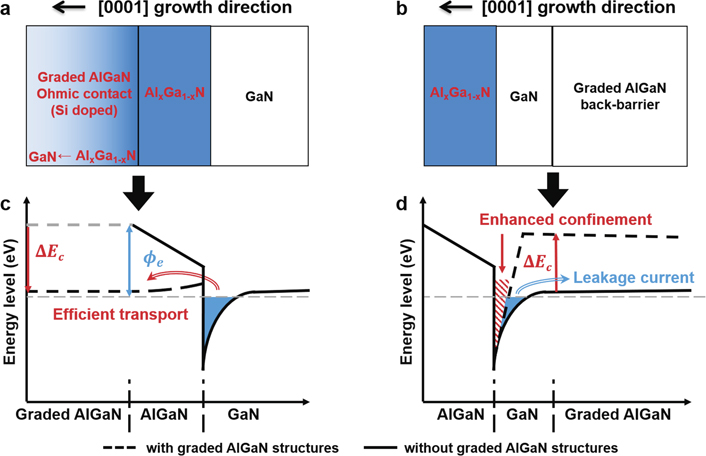
Figure 7. Band diagrams of traditional AlGaN HEMTs (solid lines) and HEMTs with additional (a) graded ohmic contact layers and (b) graded AlGaN back-barrier layers (dashed lines). Efficient carrier transport through ohmic contact, as well as enhanced electron confinement in the conductive channel can be realized by the additional graded AlGaN structures.
Download figure:
Standard image High-resolution image3. Graded AlGaN alloys for UV light-emitting device applications
In view of all the abovementioned advantages of involving AlGaN alloys in graded configurations, such graded AlGaN structures have been widely adopted in the development of AlGaN UV light emitters to control the carrier behavior in devices, including electron & hole doping, injection, confinement, and subsequent radiative recombination in the active regions. With the incorporation of graded AlGaN alloys as current injection layers, QWs, QBs, and p-EBLs have been demonstrated in UV LEDs, and the device performance, including IQE, LOP, and wall-plug efficiency (WPE), were boosted thanks to the enhanced current injection enabled by polarization-induced doping and improved carrier confinement for sufficient recombination via band engineering. Most importantly, with such effective carrier manipulation, graded-AlGaN-based device architectures exhibit great potential for the realization of UV laser diodes (LDs), in particular, electrically injected LDs, which have been intensively studied for decades but have hardly progressed. In this section, we summarize recent progress in the implementation of graded AlGaN alloys for the development of UV light emitters, including LEDs and LDs.
3.1. Graded AlGaN alloys for efficient current injection
The commonly-used acceptor impurity for p-type AlGaN alloys, Mg, requires extremely high thermal activation energies from 200 meV in GaN to 630 meV in AlN at room temperature [80]. This primarily leads to a low level of thermally activated hole concentration and highly resistive p-AlGaN current injection layers with inefficient hole injection into the active regions. An exciting breakthrough occurred when Simon et al first demonstrated a UV LED with a graded AlGaN hole injection layer [30]. The graded AlGaN layer was in-situ doped with Mg but grown on N-polar n-GaN native substrates to further enhance the doping efficiency of the polarization-induced 3DHG, since N-polar AlGaN alloys tend to possess a higher background electron density, hindering the formation of p-type conductive layers. Compared with non-graded Mg-doped p-type AlGaN layers, the graded AlGaN layers exhibited a six-fold higher hole concentration and doubled p-type conductivity at room temperature. Hence, their fabricated graded AlGaN UV LED showed a thirty times higher EL intensity at 40 mA and a greatly improved LOP.
Recently, graded AlGaN structures have been implemented in tunnel junction-based UVA LEDs emitting at ∼320 nm [32]. As shown in figure 8(a), the tunnel junction consisted of both n- and p-type graded AlGaN layers with polarization-induced 3DEG and 3DHG. When an additional impurity dopant (Mg) was doped into the graded p-AlGaN layers, hole concentrations as high as ∼1019 cm−3 were produced. Figures 8(b) and (c) separately plot the I–V curves and the WPEs of four LEDs with different Mg dopant concentrations (samples A–D). Sample C, with the highest Mg concentration (3 × 1019 cm−3), exhibited the highest current density and the maximum WPE of 1.62%, which was 103 times higher than that of sample A (without Mg doping). The external quantum efficiencies (EQEs) of samples C and D were 3% and 3.37% without an obvious droop effect. This type of graded AlGaN tunnel junction has also been implemented in UVB (290 nm) [81] and UVC (257 nm) [82] AlGaN LEDs, and their optical and electrical performances were among the highest levels for UV LEDs with similar emission wavelengths, showing the great potential of graded AlGaN-based tunneling injection for efficient UV LEDs.
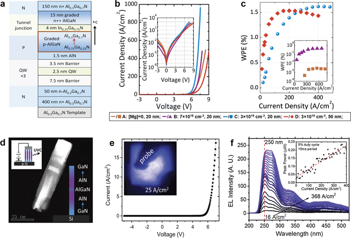
Figure 8. (a) AlGaN-based UV LED with a tunnel junction consisting of n- and p-graded AlGaN layers. (b), (c) Separate plots of the I–V curves and the WPEs of four LEDs with different Mg dopant concentrations (samples A–D). (d) Nanowire-based AlGaN UV LED with both n- and p-AlGaN current injection layer. (e) Measured I–V curves and (f) EL spectra of the fabricated nanowire UV LED. (a)–(c)Reprinted from [32], with the permission of AIP Publishing. (d)–(f) Reproduced from [36]. © IOP Publishing Ltd. All rights reserved.
Download figure:
Standard image High-resolution imageApart from conventional planar AlGaN UV LEDs, graded AlGaN alloys have also been utilized as building blocks in nanowire-based AlGaN UV LEDs [35–37]. Importantly, AlGaN nanowires can be grown on any substrate, regardless of lattice mismatch, and normally possess high crystal quality thanks to their large surface-to-volume ratios [83–85]. In addition, p-type AlGaN nanowires were found to be more conductive than thin-film AlGaN layers thanks to the reduced lattice strain imposed by surface dopants [85–87]. Therefore, such nanowire structures have emerged as an alternative device architecture for efficient UV light-emitting devices [88, 89]. Figure 8(d) shows a single AlGaN nanowire representing the device architecture of a fabricated UVC LED. The upward and downward linear grading profiles can be visually observed using the transmission electron microscopy image. The devices exhibited a low turn-on voltage of 6 V and an EL peak intensity centered at 250 nm, as displayed in figures 8(e) and (f). Additionally, a peak power of 0.22 μW at 400 mA was measured in pulsed operation mode.
3.2. The role of graded AlGaN alloys in carrier manipulation
3.2.1. Graded AlGaN structures in the active region
To facilitate the radiative recombination of electrons and holes in the active region, MQW structures are widely utilized as the active regions in AlGaN-based UV LEDs. However, researchers have recognized that the existence of strong polarization effects in AlGaN MQWs has adverse effects on the carrier confinement and recombination process, namely the notorious quantum-confined Stark effect [21]. To address this issue, active regions with incorporated linear or step-like graded AlGaN quantum structures have been proposed, which were found to be effective in the tailoring of internal polarization fields, the modulation of band structures, and therefore, the manipulation of carrier transport behavior [66–73].
Figures 9(a) and (c) illustrate the step-like graded QBs [71] and linearly graded QWs [66] used to re-engineer the energy band. Figure 9(b) plots the calculated band diagram of sample C shown in figure 9(a), namely Al0.54→0.52→0.50GaN step-like graded QBs. The raised effective barrier heights of the QBs for electrons (ϕCB) and holes (ϕVB) provided sufficient carrier confinement in the QWs for radiative recombination. Furthermore, the modulated p-EBL possessed the highest electron barrier height (ϕe) of 338.8 meV and the lowest hole barrier height (ϕh) of 358.0 meV among the three samples, indicating that such band engineering can effectively prevent electron overshooting without hindering hole injection. Following the same principles, sample B in figure 9(c) with increased-Al-composition (IAC) graded Al0.5→0.6GaN QWs was also able to effectively manipulate carrier transport and enhance carrier confinement capability. The corresponding UV LEDs exhibited the highest IQE without an obvious droop effect and a 67.04% higher LOP than reference sample A, as compared in figure 9(d).
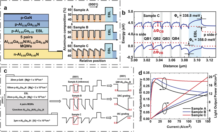
Figure 9. (a) The investigated UV LEDs with non-graded Al0.5Ga0.5N QBs (top, sample A), non-graded Al0.54Ga0.46N QBs (middle, sample B), and step-like graded Al0.54→0.52→0.50GaN QBs (bottom, sample C). (b) The calculated band diagram of sample C. (c) The investigated UV LEDs with non-graded Al0.5Ga0.5N QWs (top, sample A), reduced-Al-composition graded Al0.5→0.4GaN QWs (middle, sample B), and IAC graded Al0.5→0.6GaN QWs (bottom, sample C). (d) The IQE and LOP curves of three samples. (a), (b) © 2020. Reprinted, with permission, from [71]. (c), (d) © 2019. Reprinted, with permission, from [66].
Download figure:
Standard image High-resolution imageIn particular, the band engineering of LQBs stands out as an important realm, since such structures act as a bridge between the active regions and p-type regions of AlGaN UV LEDs. Such LQBs can deeply influence the carrier injection efficiency and confinement capability. Figure 10(a) shows three separate samples that incorporate non-graded Al0.15Ga0.85N, upward-graded Alx Ga1−x N (x = 0.15→0.3), and downward-graded Alx Ga1-x N (x = 0.3→0.15) LQBs [75]. The inset of figure 10(b) shows the UV light emission of the fabricated devices with a downward-graded LQB. The main device characteristics, including the EL intensity (figure 10(b)), IQE (figure 10(c)), and LOP (figure 10(d)) of such devices are significantly boosted, demonstrating the feasibility of this type of band engineering for efficient carrier behavior manipulation.
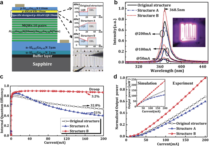
Figure 10. (a) A schematic of a UV LED with a non-graded Al0.15Ga0.85N LQB (top), an upward-graded Alx Ga1−x N (x = 0.15→0.3) LQB, and a downward-graded Alx Ga1−x N (x = 0.3→0.15) LQB. (b)–(d) Separate plots of the EL intensity, IQE, and LOP of the fabricated devices. Reproduced with permission from [75]. © The Optical Society.
Download figure:
Standard image High-resolution image3.2.2. A p-EBL in the form of a graded AlGaN structure
A p-type EBL is widely adopted in AlGaN UV LEDs to prevent electrons from overflowing the active regions and diffusing into the p-type regions. However, large valence band offsets that form between the Al-rich p-EBLs and the p-AlGaN layers can also severely block hole injection. Similarly to the graded QWs and QBs, a graded AlGaN structure has recently been adopted as a p-EBL to tailor the band structure, thereby facilitating hole injection. Figures 11(a) and (b) separately show two devices fabricated without (LED A) and with (LED B) graded p-EBLs [78]. According to numerical calculations, the modulated band structure of graded p-EBLs can lead to reduced hole energy loss, and consequently, accelerated hole injection. Simultaneously, the graded p-EBL exhibited a higher electron barrier height of 682 meV, compared with non-graded EBLs (386 meV). As a result, overflown electrons were able to be sufficiently blocked, and holes were be efficiently injected into the active regions. The measured EL spectra show that LED B had a smaller parasitic emission intensity, as compared in figure 11(c). Figures 11(d) and (e) show the improved I–V characteristics and output power of LEB B. In particular, a high EQE of 7.6% was measured, thanks to the effectiveness of the carrier transport manipulation performed by this type of band engineering. Additionally, other types of novel EBL in the form of graded AlGaN structures were demonstrated in [73, 79]. All the simulated and experimental results reveal that this type of graded AlGaN EBL can facilitate much higher hole injection efficiencies with reduced energy losses by lowering the effective hole barrier height and screening the strongly polarizing electric fields.

Figure 11. Schematic energy band diagrams for AlGaN-based UV LEDs with (a) the traditional p-EBL structure and (b) the graded AlGaN p-EBL. The measured (c) EL spectra, (d) I–V characteristics, (e) EQE, and optical power density of LED A and LED B are comprehensively compared. Reproduced with permission from [78]. © The Optical Society.
Download figure:
Standard image High-resolution image3.3. Graded AlGaN structures for UV LD implementation
In recent decades, with the enormous effort devoted to the development of AlGaN UV LEDs, remarkable progress has been achieved, including the demonstration of the shortest wavelength of 210 nm [77], the highest IQE of 92% [90], an EQE higher than 20% [91], and a large WPE of 21.6% [92]. However, the development of UV LDs has fallen behind that of LEDs. For example, electrically injected UV LDs emitting at 336 nm [93] and 342 nm [94] were reported more than a decade ago, with high operating voltages of more than 25 V in the lasing mode due to poor hole injection efficiency. To overcome these challenges, the exploration of graded AlGaN alloys by leveraging their polarization-induced carrier doping could be a promising and effective approach for enhancing current injection in UV LDs, in addition to the conventional impurity (Mg) doping technique. Moreover, such graded structures naturally possess a graded refractive index along their grading profiles, according to Vegard's law [95]. Therefore, graded AlGaN layers can be employed to enhance UV optical-mode confinement in the active regions for larger optical gains and to achieve better control of carrier behavior.
As an example, the configuration of a UV LD with a graded AlGaN layer is schematically shown in figure 12(a). A graded cladding layer is employed to enhance current injection efficiency and optical mode confinement. An additional graded AlGaN contact layer is inserted to reduce the contact resistance. Utilizing this type of device architecture, Sato et al tentatively demonstrated an electrically pumped 298 nm UV LD with a current density of 41.2 kA cm−2 [33, 96, 97]. The optical mode confinement factor was calculated to be 3.5%, as shown in figure 12(b). More excitingly, a 271.8 nm electrically pumped UV LD was recently realized based on the same structure, which is the shortest wavelength recorded for thin-film based AlGaN UV LDs [34]. The pulsed I–V characteristics shown in figure 12(c) exhibit a super-linear increase of output power above the threshold current of 0.4 A. A sharp EL spectrum peak emerges at 271.8 nm, indicating successful UV-B lasing with a pulsed current at room temperature.
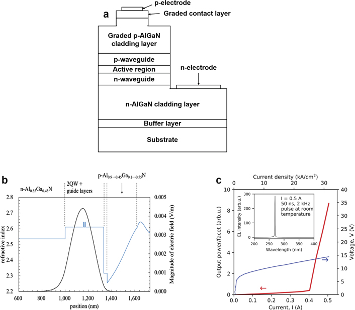
Figure 12. (a) Schematic of an AlGaN-based UV LD with a graded cladding layer. (b) Calculated refractive index and optical mode in Sato et al's investigations. (c) I–V characteristics and output power of the 271.8 nm UV LD in Zhang et al's work. The inset shows the EL spectrum centered at 271.8 nm at 0.5 A. (b) Reprinted from [33], with the permission of AIP Publishing. (c) Reproduced from [34]. © IOP Publishing Ltd. 2019 The Japan Society of Applied Physics.
Download figure:
Standard image High-resolution imageAnother recently proposed configuration with graded AlGaN alloys intended for UV LD implementation is the well-known graded-index separate confinement heterostructure (GRINSCH), which has been widely adopted as the building block of cubic III–V compounds, for example, in GaAs and InP-based LDs [98–100]. GRINSCH consists of two graded AlGaN layers on both sides of MQWs. The grading profiles are specially designed so that the refractive index is highest in the active region, where the optical mode should be well confined for UV lasing [101]. Figures 13(a) and (b) show an Al-polar GRINSCH structure and the calculated optical mode, corresponding to a high optical confinement factor of ∼13% [102]. Simultaneously, polarization-induced 3DEGs and 3DHGs can be generated in the graded AlGaN layers, leading to the automatic formation of a p–n junction in the GRINSCH structure. Figure 13(c) shows the calculated band diagram and carrier concentration of a GRINSCH structure under thermal equilibrium. Both electrons and holes have a high concentration of ∼3 × 1018 cm−3 in the p–n junction with external doping. Moreover, the AlGaN GRINSCH diode shows a turn-on voltage reduced by more than 20 V, compared with conventional UV light emitters, for the thin-film-based structure [31].
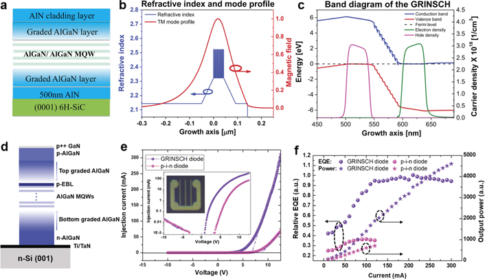
Figure 13. (a) The device structure and calculated (b) refractive index and magnetic field, (c) band diagram, and carrier concentration of a GRINSCH LD. (d) The device structure of a nanowire GRINSCH diode. (e) I–V characteristic of a GRINSCH and p-i-n diodes. The inset shows semilog I–V curves and an optical image of the tested device. (f) Measured relative EQE and output power of both devices. (a)–(c) © 2017 IEEE. Reprinted, with permission, from [102]. (d), (e) Reprinted with permission from [37]. Copyright (2018) American Chemical Society.
Download figure:
Standard image High-resolution imageAdditionally, this type of GRINSCH AlGaN UV LD has been explored in a nanowire-based device architecture, as shown in figure 13(d) [37]. The nanowires were epitaxially grown on conductive Si substrates coated with metals and then fabricated into vertically conductive devices. A large optical confinement factor of 17.9% was obtained by numerical simulation. Compared with a p-i-n diode without graded AlGaN layers, the GRINSCH diode exhibited significantly improved electron and hole concentrations, by 29.5% and 81.1%, respectively. Combining excellent carrier generation and optical mode manipulation, the GRINSCH diode had a smaller turn-on voltage (6.5 V) and a four-fold reduced series resistance compared with the p-i-n diode, as plotted in figure 13(e). Figure 13(f) demonstrates that the GRINSCH diode possessed significantly enhanced output power and EQE without an obvious droop effect.
4. Graded AlGaN alloys in power electronic devices
Even though conventional HFETs based on abrupt AlGaN/GaN heterostructures have facilitated the rapid development of power electronic devices, the pursuit of such devices for higher-frequency and higher-voltage operation requires more precise control over carrier behavior, in most cases, electron behavior in the conductive channels. Hence, we have seen the widespread implementation of graded AlGaN alloys in power electronic devices for the efficient manipulation of the carrier generation and transport processes. Specifically, graded AlGaN channels with high-density 3DEGs have been utilized either to improve linear transfer characteristics for RF applications or to enable highly conductive Al-rich AlGaN channels for high-voltage applications. Besides, graded AlGaN structures can either act as ohmic contact layers that improve electron transport through metal–semiconductor contacts, or as back-barrier layers that confine electrons in conductive channels to a sufficient extent to suppress undesired leakage current. Eventually, these types of effective polarization-induced doping and band engineering will both enhance current/power density and prevent device degradation under large bias voltages.
4.1. Graded AlGaN-based conductive channels
4.1.1. Graded AlGaN channels for linearity improvement in RF applications
AlGaN/GaN-based HEMTs have achieved great success in microwave power applications [103–107] due to their high electron mobility and large power capacity. However, conventional HEMTs with 2DEG channels inherently suffer from severe transconductance (gm
) drop-off under large gate biases (Vgs
) [24–26]. This property is detrimental to the linear transfer characteristics between input, modulated, and output signals and can introduce unwanted signal compression, offset, and intermodulation distortion into communication systems [18]. One effective approach for improving transistor linearity is to intentionally design the doping profiles in the conductive channels to tailor the gm
–Vgs
curves and thus produce a constant gm
within a wide range of bias voltages [38–42, 59]. Such principles can be realized by adopting graded AlGaN alloys, in which the 3DEG carrier profiles can be modulated according to  , as discussed in section 2. Ancona et al carried out a comprehensive numerical study of graded AlGaN channels with different grading profiles (linear, quadratic, quartic, tanh, and linear-tanh functions) for RF applications [108]. All the transistors with graded AlGaN channels, which are normally referred to as polarization-induced FETs (PolFETs), exhibited flat and bias-insensitive gm
values, compared with conventional HEMTs.
, as discussed in section 2. Ancona et al carried out a comprehensive numerical study of graded AlGaN channels with different grading profiles (linear, quadratic, quartic, tanh, and linear-tanh functions) for RF applications [108]. All the transistors with graded AlGaN channels, which are normally referred to as polarization-induced FETs (PolFETs), exhibited flat and bias-insensitive gm
values, compared with conventional HEMTs.
So far, PolFETs with linearly graded AlGaN channels have already been experimentally demonstrated, as schematically shown in figure 14(a) [38]. Figure 14(b) presents the calculated doping profiles in the linearly graded channel with different thicknesses and Al composition gradients. Uniform doping profiles are observed, which are consistent with ![$\rho \left(z\right)=\left[{P}_{A{l}_{x}G{a}_{1-x}N}-{P}_{\text{GaN}}\right]/t$](https://content.cld.iop.org/journals/0034-4885/84/4/044401/revision3/ropabde93ieqn8.gif) . The experimentally measured gm
− Vgs
curves (figure 14(c)) exhibit a constant gm
value over a wide range of bias voltages, confirming the effectiveness of doping profile manipulation for linearity improvement. Besides, the contour plots of cut-off frequency (fT
) and maximum oscillation frequency (fmax) in figures 14(d) and (e) also exhibit bias-insensitive behaviors for high-voltage operation, further proving the suitability of PolFETs with graded AlGaN channels for RF applications.
. The experimentally measured gm
− Vgs
curves (figure 14(c)) exhibit a constant gm
value over a wide range of bias voltages, confirming the effectiveness of doping profile manipulation for linearity improvement. Besides, the contour plots of cut-off frequency (fT
) and maximum oscillation frequency (fmax) in figures 14(d) and (e) also exhibit bias-insensitive behaviors for high-voltage operation, further proving the suitability of PolFETs with graded AlGaN channels for RF applications.

Figure 14. (a) Schematics of a PolFET with a graded AlGaN channel. (b) Calculated band diagrams and doping profiles in the conductive channel with different graded profiles. (c), (d) Constant gm over a wide range of bias voltages. (e), (f) Constant frequency characteristics. © 2014 IEEE. Reprinted, with permission, from [38].
Download figure:
Standard image High-resolution imageIn particular, such graded AlGaN channels are very suitable for highly scaled devices with short gate lengths and source-to-drain spacings. In such devices, electrons move at their saturated velocity (vsat) in the conductive channels and thus support a higher switching speed. However, the vsat of a 2DEG largely decreases with increased carrier density at large biases [24–26]. Since gm is proportional to vsat in short-channel devices, the RF performance of conventional HEMTs inevitably rolls off. In this regard, linearly graded AlGaN channels which can produce bias-insensitive gm are highly desirable for improving the linearity of RF applications. Figure 15(a) shows a PolFET with a gate length of 250 nm [39]. A 20 nm reversely graded AlGaN layer was employed as the contact layer for better ohmic contact. A tailored gm –Vgs curve with a flat gm as high as 240 mS mm−1 was obtained, along with flat frequency features over a wide range of drain currents, as shown in figures 15(b) and (c), respectively. Apart from laterally scaled PolFETs, a vertical device scaling scheme was proposed by Park et al [40]. They suggested incorporating a hybrid 2DEG/3DEG channel, so that the device was able to take advantage of the higher mobility of 2DEGs as well as a manipulated 3DEG doping profile. As shown in figure 15(d), the vertical PolFET had a narrow channel as thin as 8 nm [3 nm Al0.9Ga0.1N + 5 nm linearly graded AlxGa1-xN (x: 0→15%)]. The measured flat gm values indicate that the linearity was significantly improved, in comparison with a conventional HEMT with a non-graded Al0.9Ga0.1N channel, as indicated in figure 15(e). Quite recently, a scaled PolFET with a gate length of 50 nm was demonstrated, exhibiting improved fT and fmax of 170 GHz and 363 GHz, respectively, indicating the great potential of graded AlGaN-channel based PolFETs for RF applications [109].
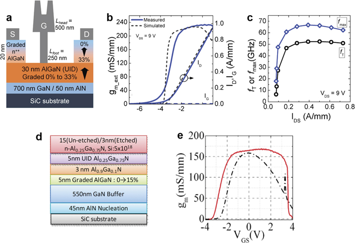
Figure 15. (a) A schematic of the laterally scaled PolFET. (b), (c) The corresponding RF performances, with greatly improved linearities. (d) A schematic of a vertically scaled PolFET with a constant gm over a wide range of applied gate voltages, shown in (e). (a)–(c) © 2017 IEEE. Reprinted, with permission, from [39]. (d), (e) Reprinted from [40], with the permission of AIP Publishing.
Download figure:
Standard image High-resolution image4.1.2. Graded AlGaN channels for high-voltage operation
Apart from the higher-frequency operation, another trend of AlGaN power electronic devices is a movement towards higher-voltage applications. Therefore, ultrawide bandgap (UWBG) AlGaN devices incorporating Al-rich AlGaN channels are emerging, aiming to simultaneously enhance the BV and improve the power capacity [110–113]. There are three main device architectures for UWBG AlGaN transistors, including impurity-doped metal-semiconductor FETs (MESFETs), 2DEG-channel HFETs, and graded AlGaN channel PolFETs. In MESFETs, the high activation energy of n-type impurity dopants in Al-rich AlGaN alloys cannot meet the requirements for highly conductive channels [80]. In addition, strong impurity scattering introduced by ionized impurities is also undesirable for achieving high electron mobility. In regard to the HFETs, the 2DEG density can be enhanced by increasing the Al composition contrast between the barrier and the channel. However, the 2DEG mobility of Al-rich HEMTs was reduced in a lower Al-composition AlGaN channel [111, 114], not to mention that 2DEGs are not suited to linear transfer behaviors in RF applications. To overcome these drawbacks in MESFETs and HEFTs, scientists have proposed and investigated PolFETs by adopting graded AlGaN channels, which can not only generate a high-density 3DEG via polarization-induced doping, but also enhance the 3DEG mobility due to the absence of impurity scattering. In particular, the 3DEG carrier profile can be manipulated by controlling the graded AlGaN alloys to improve transistor linearity. Therefore, the PolFET has emerged as a promising device architecture and has shown great potential in the UWBG AlGaN device community.
Figures 16(a)–(c) present the schematics of three UWBG AlGaN PolFETs and their corresponding output I–V curves. Figure 16(a) shows a PolFET with an average 3DEG mobility, μ, as high as 210 cm2 V−1 s−1, which was among the highest value for UWBG AlGaN transistors with Al compositions >70% [43]. However, the electron density was measured as 7 × 1017 cm−3, which was relatively low, compared with other doping strategies. Besides, the high-Al-composition AlGaN surface resulted in poor Ohmic contact characteristics. As a result, the maximum drain current (Idmax) was suppressed to only 24 mA mm−1. Figure 16(b) shows a PolFET with further improved channel mobility of 340 cm2 V−1 s−1 [44]. Besides, the higher Al composition contrast (Al0.6Ga0.4N to AlN) in the graded AlGaN alloys led to a higher 3DEG density of 1.3 × 1018 cm−3 as well as a significantly enhanced Idmax of 200 mA mm−1. Recently, Lemettinen et al demonstrated an N-polar PolFET with a graded Al0.8Ga0.2N→AlN channel for the first time, as shown in figure 16(c) [45]. The electron density was measured at 1.3 × 1018 cm−3, indicating an integrated sheet charge density as high as 1.2 × 1013 cm−2. This value is comparable to the typical 2DEG density of abrupt AlGaN heterojunctions, confirming the effectiveness of the polarization-induced doping strategy via graded structures in N-polar Al-rich AlGaN devices. The measured Idmax was 60 mA mm−1, which can be further improved by optimizing the growth and design of N-polar graded AlGaN alloys and the ohmic contacts.
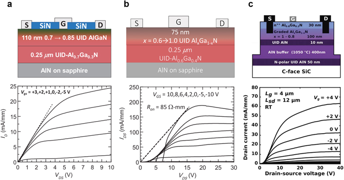
Figure 16. (a)–(c) Three schematics of UWBG PolFETs with different graded AlGaN channels, along with their corresponding I–V curves. (a) Reproduced from [43]. © IOP Publishing Ltd. 2018 The Japan Society of Applied Physics. (b) Reprinted from [44], with the permission of AIP Publishing. (c) © 2019 IEEE. Reprinted, with permission, from [45].
Download figure:
Standard image High-resolution image4.2. Graded AlGaN alloys to manipulate electron transport and confinement capability
4.2.1. Graded AlGaN ohmic contact layers for efficient electron transport
Another critical challenge faced by AlGaN HFETs is the relatively high electron barrier height formed at the surfaces of AlGaN barrier layers, especially for UWBG AlGaN transistors, due to the much smaller electron affinity of AlN (∼0.4 eV) than that of GaN (∼4.1 eV). Therefore, it is difficult to form an ohmic contact with low contact resistance. The most straightforward way to lower the electron barrier height is by decreasing the Al composition at the semiconductor's surface. Thus, downward-graded AlGaN alloys (from Al-rich to Al-less AlGaN) along the growth direction can possibly be used as additional ohmic contact layers. Such graded structures should be doped with donor impurities to compensate for the 3D negative polarization charges and to flatten the conduction band for efficient electron transport through the ohmic contacts.
Figure 17(a) represents a schematic of an AlN transistor with a graded AlGaN ohmic contact layer. This device used Ti/Al/Ni/Au metal stacks as the source and drain contacts [46]. The linear I–V curves (as shown in figure 17(b)) and enhanced current density shown in the inset confirm the formation of good ohmic contacts by the 150, 220, and 340 nm thick graded AlGaN layers. However, the 60 nm thick graded structure did not perform effectively as an ohmic contact layer, exhibiting a lower current density than the non-graded structure. As illustrated in figure 17(c), the polarization-induced charge density in a 60 nm thick graded AlGaN layer was so high that Si compensation doping was not sufficient. Consequently, a high electron barrier was formed, which severely hindered electron transport. For comparison, figure 17(d) shows the charge density and the band diagram of the 340 nm thick graded layer. The compensation doping was able to effectively neutralize the negative charges and
form a smooth conduction band. The specific contact resistance measured was as low as ∼10−2 Ω·cm2. It should be noted that the gate region should be recessed down to the AlN channels during device fabrication, as shown on the right of figure 17(a). The large electron barrier height formed at the AlN channel's surface can suppress undesired gate leakage current and benefit the formation of a good Schottky contact at the gate region.

Figure 17. (a) A schematic of the AlN transistor with a graded AlGaN ohmic contact layer. (b) I–V curves and current densities of the fabricated ohmic contacts with 60, 150, 220, and 340 nm thick graded contact layers and without a graded AlGaN layer. (c), (d) The calculated charge density and band diagrams of the 60 nm and 340 nm thick graded AlGaN ohmic contact layers. Reprinted from [46], with the permission of AIP Publishing.
Download figure:
Standard image High-resolution imageOwing to the successful electron transport manipulation via band engineering, this type of graded AlGaN ohmic contact layer has attracted extensive attention as a building block for UWBG AlGaN transistors to improve the contact characteristics [47–51]. Figures 18(b) and (c) separately show the band diagrams of a PolFET (figure 18(a)) without and with the incorporation of a graded AlGaN ohmic contact layer [47]. It can clearly be seen that the electron barrier height at the semiconductor's surface was significantly reduced and that the conduction band was flat for efficient electron transport, thanks to the incorporation of the graded contact layer. The measured contact resistance of this PolFET was 73 mΩ·mm. Figure 18(d) shows a fabricated Al0.7Ga0.3N/Al0.5Ga0.5N HFET with a recessed gate region [51]. Figures 18(e) and (f) are separate the band diagrams of the gate Schottky contact with a raised barrier height and their source/drain ohmic contact with a specific contact resistance of 6.2 × 10⁻⁵ Ω·cm2. Besides, an MESFET with a downward-graded AlGaN contact layer also exhibited a low specific contact resistance, which was measured at 3.3 × 10⁻⁵ Ω·cm2. All these values represent the lowest reported contact resistance for Al-rich AlGaN channel transistors, suggesting the excellent carrier transport manipulation of graded AlGaN alloys via band engineering for ohmic contact applications.

Figure 18. (a) The schematic of a PolFET with a graded AlGaN ohmic contact layer; (b), (c) separate calculated band diagrams of structures without and with a graded layer. (d) A schematic of an Al0.7Ga0.3N/Al0.5Ga0.5N HFET with a recessed gate region. (e), (f) Separate band diagrams at the gate and source/drain regions with ideal contact characteristics. (a)–(c) © 2015 IEEE. Reprinted, with permission, from [47]. (d)–(f) Reprinted from [51], Copyright (2020), with permission from Elsevier.
Download figure:
Standard image High-resolution image4.2.2. Graded AlGaN back-barrier layers for sufficient electron confinement
Back-barrier layers act as an important device architecture in AlGaN HEMTs to confine electrons inside conductive channels and thus suppress leakage current at large bias voltages, preventing early device punchthrough and mitigating short-channel effects [27]. Graded AlGaN alloys have band structures that can be tuned by designing their grading profiles and which can be utilized as back-barrier layers to lift the electron barrier height beneath the 2DEG channels and thus improve the electron confinement capacity [115–117]. Figure 19(a) shows AlGaN/GaN HEMTs fabricated on a graded AlGaN back-barrier (called Str_A) and a non-graded AlGaN back-barrier (called Str_B), and their calculated electron distributions and BVs in the buffer layer. Apparently, less leakage current was observed in Str_A, confirming the effectiveness of an increased back-barrier height for carrier confinement. Therefore, the BVs of Str_A were significantly enhanced, as shown in figure 19(b). Furthermore, with increased buffer layer thickness, the BV can be further enhanced to 350 V. Additionally, it has been confirmed that graded AlGaN buffer layers can simultaneously improve the crystal quality by modulating the internal strain [118–121]. Therefore, this type of graded AlGaN back-barrier layer has been widely implemented in AlGaN electronic devices on Si [122–124], SiC [125], and sapphire substrates [126–128], contributing to the improved crystal quality of AlGaN epilayers and enhanced device performance.

Figure 19. (a), (b) The calculated electron distributions and BVs of HEMTs on graded and non-graded AlGaN buffer layers. (a), (b) Reproduced from [117]. © IOP Publishing Ltd. All rights reserved.
Download figure:
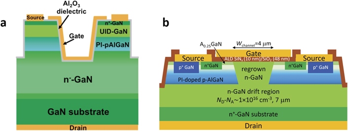
Standard image High-resolution imageMoreover, the graded p-AlGaN back-barrier layers have lately been employed in vertically conductive power devices, including trench MOSFETs [129] (figure 20(a)) and vertical double-diffused MOS (VDMOS) devices [130] (figure 20(b)). Such vertical devices consist of thick drift layers for vertical carrier transport and high voltage endurance. However, the trade-off between BV and specific on-resistance (Ron,sp) of the drift layers persists as a limitation for those devices [131–133]. Fortunately, with an inserted polarization-doped graded p-AlGaN layer (PI-doped p-AlGaN), the back-barrier height beneath the source/n-GaN region can be effectively elevated, suppressing leakage current through the p-type region into the n-GaN drift layer. Plus, 3DHGs in the linearly graded layer are uniformly distributed, so that the charge crowding effect at the p–n junctions can be avoided [134]. Combining the modulated band diagram and optimized carrier distribution, the introduction of graded p-AlGaN back-barrier layers can enhance the critical electric fields of vertical power devices for higher-voltage applications.
Figure 20. Schematics of vertical power devices with graded AlGaN drift layers including (a) trench MOSFETs, and (b) VDMOS. (a) © 2018 IEEE. Reprinted, with permission, from [129]. (b) Reproduced from [130]. © IOP Publishing Ltd. 2019 The Japan Society of Applied Physics.
Download figure:
Standard image High-resolution image
5. Conclusions and outlook
In summary, compositionally graded AlGaN alloys have demonstrated excellent abilities for effectively manipulating carrier behavior, including carrier generation control via polarization-induced doping and carrier transport control via band engineering. Therefore, such graded AlGaN structures have been intensively explored and widely adopted as the building blocks of the AlGaN-based UV optoelectronic and power electronic devices. In this review, the underlying mechanisms of graded AlGaN alloys for carrier behavior manipulation, together with the recent progress of such structures in device applications, have been comprehensively analyzed and summarized. UV LEDs/LDs and AlGaN transistors incorporating graded AlGaN structures exhibited superior device performance, as categorized in table 1, showing the exciting progress enabled by successful carrier behavior manipulation. Based on the discussions, some key advances should be noted and recognized. (1) Efficient polarization-induced doping of the graded p-AlGaN cladding layer facilitated the electrically pumped UV LDs with the shortest ever reported wavelength of 271.8 nm. (2) Sufficient carrier confinement and injection enabled by graded AlGaN quantum structures (QWs, QBs, EBLs) in UV LEDs can significantly boost the quantum efficiency and output power. (3) AlGaN transistors with graded AlGaN structures acting as conductive channels, ohmic contact layers, and back-barrier layers have exhibited improved current density, breakdown voltage, and linear transfer characteristics for higher-frequency and higher-powered operation. Therefore, there is no doubt that all the investigations carried out in recent years have significantly advanced the field of AlGaN-based optoelectronic and power devices, offering us great hope of utilizing graded AlGaN alloys to overcome the bottlenecks mentioned at the beginning of this report and to further boost device performance for advanced applications.
Table 1. Summary of optoelectronic devices (UV LEDs and UV LDs) and power electronic devices (FETs) with the incorporation of graded AlGaN alloys as key building blocks for the advancement of their performance.

|
Although great progress has been made in exploring efficient AlGaN-based devices with the incorporation of graded AlGaN structures, difficult challenges remain on many fronts, mainly including (1) material synthesis/growth; (2) device design and structural innovation. From a material growth perspective, the growth techniques/approaches for graded AlGaN alloys have not been fully developed, compared with those of conventional non-graded alloys. So far, only the linearly graded and step-like graded AlGaN structures have been preliminarily investigated and experimentally realized, while the synthesis of complicated grading profiles (e.g., parabolic, quadratic, tanh, etc.) still lack exploration, not to mention the comprehensive characterization of their crystalline quality and optical/electrical properties in device applications. Therefore, precise control of the grading profile and improvements in the crystalline quality of such graded structures are the two imperative prerequisites for fully unleashing the potential of graded AlGaN alloys and promoting them in further device exploration and implementation:
First of all, one of the challenges in the growth of AlGaN alloys with desirable grading profiles lies in the synthesis of ultra-thin AlGaN layers with accurate Al compositions. In particular, when it comes to the growth of high-Al-composition AlGaN layers, the relatively low surface mobility of Al adatoms normally results in an epilayer with a rough interface and a non-uniform distribution of Al composition. Therefore, during the growth of graded AlGaN alloys via commonly used tools such as MBE and MOCVD, the source flow sequence and the ratio of sources in the growth chamber are the key factors to be optimized. Fortunately, in the MBE system, the Al/Ga sources are generally supplied by rapidly switching on/off the shutters in front of the effusion cells. The shutters can be rapidly and precisely software-controlled and therefore, high-quality ultra-thin AlGaN layers with accurate Al compositions may be realized [3, 135, 136]. As for the MOCVD system, a pulsed-mode growth technique could be employed for the growth of monolayer (ML)-thick AlGaN structures. This special method employs a growth scheme with alternate pulses of Al/Ga sources (typically trimethyl aluminum and trimethyl gallium, TMA/TMG) and a carrier gas (such as H2 or N2) in each cycle [137, 138]. Thereby, a layer-by-layer growth mode of AlGaN alloys might be realized to produce ultrathin AlGaN structures with sharp interfaces. Consequently, by stacking these AlGaN MLs with specially designed Al compositions, we could possibly tailor the grading profiles in the AlGaN structures of the future.
Secondly, apart from grading profiles, another vital factor that influences carrier behavior manipulation is control of the crystal quality of graded AlGaN alloys, which is also the foundation for building high-performance opto- and power electronic devices. Scientists have confirmed that a graded AlGaN layer can not only affect carrier generation and transport, but can also realize strain relaxation and defect annihilation, and therefore prevent threading dislocations from reaching the conductive channels in HEMTs, or the active regions of UV emitters during the growth of AlGaN epilayers on foreign substrates (sapphire [128], Si [139, 140], SiC [101], etc.). Notably, these studies mainly focus on Al-polar structures, whereas the investigation of N-polar graded AlGaN alloys is at a very preliminary stage, which offers opportunities to explore their carrier behaviors and crystal quality control capabilities for device implementation. Furthermore, with the advent of emerging growth monitoring tools, such as coherent x-ray spectroscopy for the in-situ investigation of growth fronts [141], we are able to further understand the thermodynamics and kinetics of Al/Ga atoms during the formation of graded AlGaN alloys, which definitely benefits the realization of high-quality graded AlGaN alloys with accurate grading profiles.
Beyond the aforementioned material challenges and opportunities, from a device perspective, a carefully and reasonably designed device architecture is of great importance to fully demonstrate efficient carrier behavior control via graded AlGaN alloys: on the one hand, the carrier concentration, mobility, and distribution of polarization-induced 3DEGs/3DHGs can be significantly influenced by impurity dopants, defects, and surface states [20]. These factors should be carefully optimized and controlled to enhance carrier doping efficiency and thus current injection efficiency in AlGaN-based devices to a satisfactory level; on the other hand, carrier injection and confinement manipulation require smart and effective band engineering by constructing the graded AlGaN layers with suitable thicknesses, Al compositions, and grading schemes [21]. Notably, even though a variety of AlGaN-based opto- and power electronic devices with graded AlGaN structures have been demonstrated, there is still a great deal of room for device architectural innovation. For example, in the application of transistors, we can possibly realize a high-performance p-type doped transistor by introducing a downward-graded AlGaN channel with 3DHG, which might be utilized in the design of a complementary GaN-based transistor for power-switching applications [142, 143]. Besides, we can borrow graded MQW-like structures from UV light emitters as conductive channels, resulting in multiple 3DEG conductive channels which may realize well-tailored transfer characteristics for RF applications. In the field of UV optoelectronic devices, we can implement the graded AlGaN ohmic contact layers which are widely used in UWBG AlGaN transistors to reduce n- and p-type contact resistance and simultaneously avoid undesired UV light absorption.
In summary, it is well worth performing further investigations into the device design, fabrication, and circuit/system-level integration of optoelectronic and power electronic devices incorporating graded AlGaN alloys for the future construction of high-powered, highly efficient, and energy-saving AlGaN-based device platforms. More importantly, the successful implementation of such graded AlGaN structures may inspire the III–V and II–VI-based compound semiconductor communities to redesign their device architectures by incorporating graded configurations to boost various aspects of device performance.
Acknowledgments
This work was funded by the National Natural Science Foundation of China (Grant Nos. 51961145110, 61905236), the Chinese Academy of Sciences (Grant No. KJ2100230003), the Fundamental Research Funds for the Central Universities (Grant No. WK2100230020), the USTC Research Funds of the Double First-Class Initiative (Grant No. YD3480002002), and partially carried out at the USTC Center for Micro and Nanoscale Research and Fabrication.
Biographies
Prof. Haiding Sun received his Ph.D. in Electrical Engineering from Boston University. He is a professor at University of Science and Technology of China. He has published more than 75 peer-reviewed SCI-index journal papers including Advanced Functional Materials, Nano Letters, Nano Energy, ACS Photonics, IEEE Electron Device Letters, Applied Physics Letters, etc. His research interests include the investigation of the physics, MBE and MOCVD epitaxy, fabrication, and characterization of semiconductor materials and devices. This includes nanostructures and low-dimensional structures (quantum wires, dots, wells) for nanoelectronics and nanophotonics, based on group III-Nitrides and III-Oxides. He is a Senior Member of IEEE.
Haochen Zhang received the B.S. degree from Soochow University, Suzhou, China. He is currently pursuing the M.S. degree with the School of Microelectronics, University of Science and Technology of China, Hefei, China. His research interests include the investigation of the physics, fabrication, and characterization of III-nitride-based power electronics and photonics integrated circuits.