

Abstract
Atmospheric pressure nanosecond repetitive pulsed discharges are of interest for applications in combustion, material processing, plasma medicine and gas treatment. In this paper the observation of a hollow structure at the ignition stage of such discharge in a pin–pin geometry is reported. Plasma images show that the phenomenon occurs in a variety of gases (helium, humid helium, argon and air) suggesting that it is in first approximation non-species specific. The phenomenon is investigated in detail in pure helium discharges for peak applied voltages between 3 and 6 kV and 200 ns voltage pulse duration by performing time-resolved optical emission spectroscopy measurements of electron density, gas temperature and electric field. All the measurements were performed at the mid-gap during the early stages of the discharge, near the breakdown. The transition from a homogeneous filament to a hollow structure occurs between 4 and 5 kV in helium. Electron density measurements by Stark broadening of the He I line at 492.2 nm show no significant difference in electron densities for the applied voltage between 3 and 6 kV. In all cases, a maximum electron density of about 3.5 × 10²¹ m−3 was found. Electric field measurements performed by Stark polarization spectroscopy of the He I transition at 492.2 nm and of its forbidden counterpart show electric field strengths higher than the DC breakdown field of helium at atmospheric pressure consistent with the generation of the discharges with overvoltage. Moreover, a correlation between electric field values and the appearance of the hollow structure is observed and, remarkably, the phenomenon is not sensitive to the pre-ionization level (memory effect). Possible mechanisms for the phenomenon are discussed.
Export citation and abstract BibTeX RIS
1. Introduction
Over the last decade, a large amount of studies on nanosecond repetitive pulsed discharges have been reported. These discharges have properties that can be exploited in multiple applications including combustion [1–3], material processing [4], plasma medicine [5] and gas treatment [6–8], owing to the efficient generation of key reactive species (O, H, N, OH, NO...) and UV photons.
Nonetheless many aspects of the fundamental kinetic mechanisms of these discharges remain elusive. For instance, recent experimental and modeling results [9–11] have demonstrated the occurrence of the so-called fast gas heating mechanisms in air discharges. More specifically, an increase of the gas temperature by hundreds of Kelvin within a few tens of nanoseconds was observed. This phenomenon in air results from dissociative quenching of molecular oxygen by electronically excited states of N2 (N2 (B, C)) following their generation by electron impact excitation of N2 during the discharge [10]. The generation of atomic oxygen is accompanied with a fast heat release due to the much higher excitation energy of N2 (B, C) compared to the binding energy of O2. This effect has been observed at atmospheric and reduced pressures in air and in fuel-air mixtures [12]. Potential fast gas heating in other gases than air has not received much attention so far. Shock-waves generation resulting from the fast heat release has also been reported [13]. For example, Stepanyan et al showed the radial propagation of torus-shaped thermal jets with velocities up to 30 m s−1 following a single spark discharge in air [14]. They also observed a similar effect in CH4-air mixtures, nitrogen and in argon. These jets have direct implications for plasma-assisted combustion for which the generation and transport of radical species enhancing combustion is a key determining factor of their effectiveness.
Fast ionization mechanisms during the breakdown process in atmospheric pressure air nanosecond pulsed discharges have also been investigated [15]. Differences in streamer velocities, radius, and propagation lengths have been observed depending on the applied voltage polarity, peak voltage amplitude and voltage rise time. It is well established that positive streamers are easier to initiate (lower applied voltage required) than negative streamers and propagate faster. This is due to the increase in radius of negative streamers compared to positive streamers as they propagate in the same direction than electrons drift. A larger streamer radius leads to a reduced field enhancement in the streamer head [16].
It has also been observed that discharges generated by voltages in excess of the breakdown voltage (overvoltage) using voltage pulses with a fast rise time can result in more homogeneous and diffuse discharges [17–20]. Uniformity of the discharges generated by fast rise time voltage pulses was attributed to pre-ionization of the gas ahead of the streamer front by fast runaway electrons and x-rays [20–22]. The mechanism of runaway electrons generation involves very high electric fields enabling the acceleration of electrons to very high energies.
The breakdown process and plasma dynamics of discharges generated with overvoltage hence differ from those of discharges generated without overvoltage. Simeni Simeni et al performed 200 ps time resolution electric field measurements during breakdown in a nanosecond discharge in atmospheric pressure air generated by fast rising voltage pulses (3 kV ns−1 voltage pulse rise rate) measured an electric field value at breakdown of about 75 kV cm−1, much higher than the 30 kV cm−1 predicted by the Paschen law for a DC breakdown in air at atmospheric pressure [23]. The measurements were performed at the center of the diffuse discharge. The same work also reported that a very high breakdown field resulted in a very rapid electric field reduction after breakdown (within few nanoseconds) due to plasma self-shielding following charge separation. Overvoltage can be achieved when the voltage pulse rise time is faster than the rate of ionization. Consequently, measurements performed with a voltage rise rate of only about 0.1 kV ns−1 showed a breakdown field in air at atmospheric pressure of about 32 kV cm−1 [24], closer to the breakdown threshold predicted by the Paschen law. A slower field reduction after breakdown (within tens of nanoseconds) was also measured.
Pin–pin discharges are very easily reproducible in time and space and have been studied in considerable detail. Previous work on these discharges in air/nitrogen include measurements and production of reactive species such as NO [25, 26], O [27], N2 (A, B, C) [27], N2 (v = 0−9) [28], N [25], electron densities [10]. In addition to a detailed study of the plasma kinetics of nanosecond pulsed plasmas in argon [29], OH density measurements in He–H2O [30], in N2–H2O mixtures [31] and in water vapor [32] have been reported.
In this work we report on the dynamics during the breakdown phase of helium pin–pin atmospheric pressure nanosecond discharges generated with overvoltages and focus on the observed hollow structure of the plasma. We also show that the phenomenon occurs in humid helium, argon and air pulsed plasmas. Previously such phenomenon has been observed in pinched plasmas [33] and in plasma bullets [34], but the latter is due to gradients in gas composition in the jet effluent [35, 36].
2. Experimental setup and measurement methods
Figure 1 shows a schematic of the experimental setup. The discharge was produced between two tungsten pin electrodes separated by a gap distance of 4.2 mm. The upper and bottom electrodes were circular cylinders with diameters of 1 and 3.2 mm, respectively, and have tapered tips with a radius of ∼0.15 mm. The chamber was pumped down and filled three times with the gas before the discharge was generated and experiments were performed. The flow rate was kept constant at 1 l min−1. The gas outlet opened to ambient air was controlled by an overpressure valve in order to maintain the pressure of the chamber constant at ∼1 atm. In this experiment, the discharge was generated in three different gases and one gas mixture (helium, argon, air and humid helium). The discharge in helium (see image in figure 1) is the main focus of this work because of the low applied voltage required to sustain a reproducible discharge, providing us a large range of available over-voltage conditions. In addition, discharges in helium are more diffuse and stable while exhibiting less contraction.
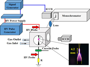
Figure 1. Schematic of experimental setup, OES diagnostic system and an image of the helium nanosecond pulsed discharge.
Download figure:
Standard image High-resolution imageA high-voltage pulse generated by a NPG-18/3500 (Megaimpulse: Modern Semiconductor Technologies) was transferred to the upper pin via a matched 75 Ohm transmission line. The pulse amplitude used was 15 kV with a pulse duration of 6 ns FWHM. A resistor of R = 72.5 Ω was placed between the bottom pin and the ground to avoid a short cut and drop in impedance significantly below 75 Ω. The other high-voltage pulser used (DEI PVX-4110) had a maximum voltage of 10 kV and a minimum pulse duration of 200 ns. The high-voltage was delivered to the 10 kV pulser by a DC high-voltage power supply (Spellman SL150). This pulser was only used to study helium discharges. A Tektronix AFG 3022B function generator with a fixed repetition frequency of 1 kHz triggers the pulser. The 72.5 Ω resistor was replaced by a 1 kΩ resistor to limit the current of the 10 kV pulser.
The voltage across the pins was measured using two high voltage probes (Tektronix P6015A) and the current was recorded using a Rogowski coil (Pearson electronics 2878) placed between the bottom pin and the resistor. The voltage and current waveforms were recorded by a digital oscilloscope (RIGOL DS 1204B). By measuring the current on the low voltage side we exclude the displacement current. The delay Δt between the voltage and current probes was obtained by measuring the current and voltage across a vacuum capacitor. A time delay of the voltage probe compared with the current probe of Δt = −4.4 ns was found and corrected for. In this work, t = 0 ns was defined as the time when the voltage pulse reaches an amplitude of 0.75 kV.
The evolution of the discharge morphology was studied by taking time and spatially resolved images with an intensified charged coupled device (ICCD Andor iStar DH340T-25U-3) coupled with a lens (UV-Nikkor 105 mm f/4.5). The minimum exposure time of the ICCD camera was 3 ns. The ICCD camera was triggered by the TTL output signal from the same function generator as the power supply. Single shot images were taken with different delay times realized by the internal delay generator of the ICCD camera.
An imaging lens (UV-NIR Achromatic Triple Lens, f = 90 mm) was used to focus the axial plane of the pin–pin discharge onto the entrance slit of a monochromator (ARC AM510, f = 1000 mm) with no magnification (1:1). The monochromator is equipped with a grating of 1800 grooves mm−1 and a 50 μm entrance slit width was used. Time-resolved optical emission spectra were recorded by the same ICCD as used for imaging, mounted on the exit port of the monochromator with a spectral resolution of ∼35 pm. The instrumental broadening profile is in good approximation Gaussian. A plastic polarizer plate was inserted in front of the entrance slit of the spectrometer in order to perform electric field measurements using Stark polarization emission spectroscopy. The polarizer was aligned such that it only transmits light from the plasma which is polarized in the axial electric field direction (vertical direction). The vertical component of the electric field is measured in this configuration.
Electric field measurements as well as all the other spectroscopic diagnostics were performed at the center position between the two needles.
2.1. Gas temperature
Time-resolved gas temperature measurements at the mid-gap were performed by recording the ro-vibrational emission spectra of the second positive system N2(C3Πu–B3Πg) with its bandhead at 337.1 nm. The emission finds its origin in the excitation of N2 impurities present in the discharge chamber. In atmospheric pressure helium discharges, the effective lifetime of the N2(C) state is not much reduced by quenching in helium, and thus the rotational energy transfer time is much smaller than the effective lifetime of the N2(C) state. Consequently, the rotational temperature Trot of the C state of N2 is a good indicator of the gas temperature Tg for helium plasmas [37, 38], i.e. Trot = Tg. Trot was obtained by fitting the normalized experimentally recorded spectra to the normalized simulated one obtained from Specair [39]. All emission spectra of N2(C3Πu–B3Πg) in this work were recorded with 10 000 accumulations and an exposure time of 5 ns.
2.2. Electron density
The electron density of discharges is usually determined from the Stark broadening of atomic emission lines [40]. The measured emission line profile is a convolution of the Gaussian and Lorentzian components, resulting in a Voigt function. The Gaussian broadening is due to the instrumental and Doppler broadening, while the Lorentzian broadening is due to the Stark, van der Waals and resonance broadening effects. Therefore, the Stark broadening width was obtained by deconvolution of the recorded line profile.
2.3. Stark broadening
In pure helium discharges, the emission of the Balmer series transitions of hydrogen atoms is often not present or is too weak for estimating the electron density via Stark broadening of Lara et al performed computer simulations of the Stark broadening of the He I line profile at 492.2 nm. The reported calculations take into account ion dynamics effect and the influence of electron and gas temperatures [41]. They found that at low electron densities (1019 m−3 < ne < 1022 m−3), only the allowed component He I (1s2p1P1–1s4d1D2) width contributes to the line broadening at least in a E-field free situation. This is because of the low emission intensity of the forbidden component He I (1s2p1P1–1s4f1F3) for these conditions. Lara et al introduced the reduced mass parameter μ* to characterize the non-equilibrium between electrons and heavy particles for the helium line profile [41]. In their supplementary data, the reported simulation result for μ* = 10 and Te = 1 eV is the closest to our experimental conditions. The full width at half maximum (FWHM) due to Stark effect, ΔλS in units of nm, was extracted from the simulated line profile and is expressed as a function of ne:
with ne, the electron density, in units of m−3. The time-resolved spectra of He I line were recorded with an accumulation over 15 000 pulses and an exposure time of 5 ns.
2.4. Van der Waals broadening
Van der Waals broadening is caused by the dipole interaction of the radiator with neutral ground state perturbers [40, 43]. The FWHM of this broadening mechanism in units of nm can be written as [43]:
with λ0, the wavelength in units of nm, α, the value of polarizability of the pertuber, in units of cm−3,  the difference of the squares of coordinate vectors of the upper and lower level
  Tg, the gas temperature in units of K, μ the reduced mass in units of amu and N, the density of neutral particle in units of cm−3. For the transition He I (1s2p1P1–1s4d1D2), recorded in the helium plasma we took: λ0 = 492.19 nm, α = 2.05 × 10⁻²⁵ cm−3, and μ = 2.
  can be calculated from formula in [43] using the parameters reported in the NIST database [44]. Substituting these values into the equation (2), one obtains
2.5. Resonance broadening
The He I line at 492.2 nm has significant resonance broadening. Resonance broadening occurs when the radiator interacts with the same species and either the upper or lower level of the transition has a dipole-allowed transition to the ground state. The formula for the FWHM due to resonance broadening in units of nm is given as
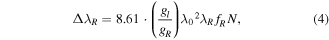
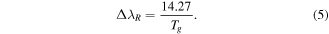
with λ0 and λR the wavelength of radiator and resonance transition in units of nm, gl and gR the statistical weights of the ground state and the upper resonance level and fR the absorption oscillator strength of the resonance transition [43]. The resonance transition is from the 1 s2p1P1 to 1s2 1S0 state for the helium line at 492.2 nm, corresponding to λR = 58.43 nm [44]. The resulting FWHM of the resonance broadening contribution for the He I line at 492.2 nm (in nm) is
The Doppler broadening width in the discharge reported in this paper (Tg < 500 K) is smaller than 4 pm and can be neglected compared to the instrumental function.
We have compared the Balmer Hβ line Stark broadening, with the Stark broadening of He I at 492.2 nm in He + 2.3% H2O and the obtained electron densities was the same within the experimental accuracy.
2.6. Electric field measurement
The electric field strength was determined using Stark polarization emission spectroscopy, which is based on the Stark effect [45–49]. π-components of each transition polarized in the electric field direction are sensitive to the change in electric field amplitude. The helium lines at 492.2 nm are the most widely used to measure the electric field because of their high sensitivity to changes in electric field amplitudes. The wavelength separation ΔλAF (in nm) between the π-components of allowed (1s2p1P1–1s4d1D2) and forbidden (1s2p1P1–1s4f1F3) lines due to the Stark effect can be correlated with the electric field:
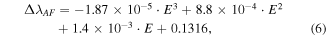
with E the electric field in units of kV cm−1 [47]. At atmospheric pressure, pressure broadening of the allowed and forbidden lines reduce the accuracy of this method. For a gas temperature lower than 500 K, the total width of the resonance and van der Waals broadenings is larger than 53 pm. Moreover, large electrons densities increase the line width due to Stark broadening in the pin-to-pin discharge and the line profile cannot be fully resolved. The wavelength resolution of the spectrometer system is about 7 pm/pixel resulting in an uncertainty of the peaks positions, which lead to an uncertainty on the measured field value of 0.7 kV cm−1. The total uncertainty of this approach due to the above described effects is estimated to be larger than 1.0 kV cm−1 and as a result this approach was not used in this work.
Obradović and Kuraica proposed another method for electric field measurements based on the ratio of the spectrally integrated intensities of the π-components of the forbidden and allowed components of the helium line at 492.2 nm [46]. The theoretical calculated relationship between the intensity ratio and the electric field between 1 and 20 kV cm−1 is shown in figure 4 of [46]. The intensity of the lines is the area under the line profile calculated by a Voigt fit. The uncertainty of this method is less than 0.5 kV cm−1 for our experimental conditions and was used in this work. A third order polynomial fit of the relation between the electric field in units of kV cm−1 and the ratio IF/IA is given by:
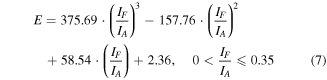
with IF and IA the spectrally integrated intensities of the forbidden and allowed components, respectively.
3. Results and discussion
Figure 2(a) shows time-resolved images during the breakdown phase of the pin-to-pin discharges in different gases, i.e. He, He+2.3%H2O, Ar and air, generated by a high applied voltage with an amplitude of 15 kV and a duration of 6 ns. The corresponding voltage and current waveforms for the helium discharge are shown in figure 2(b). The current and voltage waveforms are very similar to those in the other gases. All the images (A)–(C) are taken in a time sequence which corresponds to the indicators (A)–(C) in figure 2(b) with an uncertainty of 2 ns due to the jitter of the voltage pulse relatively to the camera gate. As observed in figure 2(a) the discharge evolution in time displays a hollow structure very early in time, close to the first observable light at breakdown. The hollow structure is observed during the fast rise of the discharge current. Then within a few nanoseconds (≤3 ns), after the peak of the current is reached, the plasma fills the entire gap and a strong emission intensity (images B and C) is observed. This is the case for all the investigated gases. In all the investigated gases the hollow structure is characterized by a weak emission intensity at the moment in time of the hollow profile. We were unable to resolve the ionization dynamics underpinning the formation of this hollow structure with the 3 ns time-resolution of our imaging system. In addition, the transient phenomenon was found to be dependent on both triggering strategy and electrode geometry. Hollow profiles were observed using the 'kinetic series' mode imaging of single shot images but were not able to be obtained when using accumulated imaging. This suggests that the phenomenon occurs on a time scale similar or even smaller than the time scale of the jitter associated with plasma generation. The phenomenon seems also to be sensitive to experimental conditions. The hollow structures were observed for a repetition rate between 0.2 Hz and 1 kHz and in all the investigated gases, suggesting that the underpinning mechanism responsible for the hollow structure is in first approximation gas independent. The pre-ionization remaining from the previous discharge seems not to contribute to the phenomenon as a first order effect.
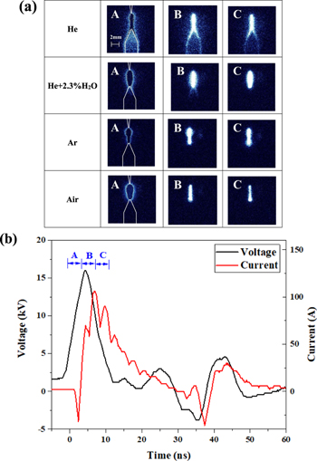
Figure 2. (a) Time-resolved images of the emission of a discharge generated by a 10 ns voltage pulse with an amplitude of 15 kV. The voltage rise rate is about 2.54 kV ns−1. The pulse repetition rate is 10 Hz. The exposure time of the signal shot images is 3 ns. (b) Applied voltage and current waveforms of the helium nanosecond pulsed discharge. The indications A, B, C in the images relate to the indicated time interval on the current–voltage waveform graph.
Download figure:
Standard image High-resolution imageWhile in air or argon gas, the discharges produced at relative low applied voltages (<10 kV) are not stable, in helium the discharge is sustainable and stable for a wider range of applied voltages down to 2 kV. However a minimum frequency of 10 Hz is required for a stable discharge at applied voltages lower than 4 kV. Therefore, helium was chosen for a more detailed study of the mechanism causing the formation of the hollow structure. Images in figure 3 show the temporal evolution of helium pin–pin nanosecond pulsed discharges for four different applied voltages during the gas breakdown. At 3 kV, the discharge column is readily apparent between the two pins and the emission intensity increases gradually as the conductive current increases, as shown in figure 4(a). The breakdown phase consists of an ionization front propagating toward the ground electrode (cathode directed streamer) within few nanoseconds [50]. When the applied voltage increases from 4 to 5 kV or higher, a hollow structure in the light emission appears before the formation of the spark discharge channel. The size of the hollow region increases with increasing voltage amplitude. This shows that the appearance of the hollow structure relates to the applied voltage and (hence corresponding electric field) with the threshold voltage being around 4 kV. The corresponding discharge voltage, conduction current and power waveforms of the discharges are shown in figures 4(a) and (b), respectively. Similarly to the 10 ns voltage pulse, the jitter for the 200 ns voltage pulse is also about 2 ns. The DC breakdown field predicted by the Paschen law in atmospheric pressure helium is about 4 kV cm−1 [51], which corresponds to a breakdown voltage of about 1.6 kV for the 4.2 mm gap distance. The discharges are thus ignited with overvoltage as the applied voltages at which the current waveforms start rising is significantly larger (see figure 4(a)). The delay between the voltage rise and the breakdown event (corresponding to the rise in current) decreases with increasing current. This leads to a fast increase in the deposited power for applied voltages over 4 kV giving rise to fast ionization and an increase in thickness of the plasma filaments (see figure 3). The increase in thickness of streamers has been previously reported for high overvoltages in air by Briels et al [15]. Such higher deposited power during the gas breakdown might produce gas heating. After 80 ns, the power waveform is in good approximation independent of the applied voltage. The energy deposited per pulse increases (mainly due to the increase in power during the first 80 ns) from 215 to 516 μJ with increasing applied voltage from 3 to 6 kV due to the overshoot in power.
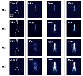
Figure 3. Time-resolved single shot images of the emission of the helium discharge with exposure time of 5 ns for different applied voltages. The corresponding voltage and current waveforms are shown in figure 4(a). The voltage rise rate is ∼0.13 kV ns−1. The pulse repetition rate is 1 kHz.
Download figure:
Standard image High-resolution image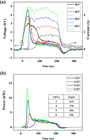
Figure 4. (a) Voltage (solid line) and current (dotted line) waveforms of helium discharges, (b) power waveform and energy deposited per pulse. The accuracy of the energy is 5%.
Download figure:
Standard image High-resolution imageThe time-resolved gas temperature of the discharge is obtained from the rotational temperature of N2(C), (B) by comparing the experimental time-resolved spectra with the simulated spectra obtained from Specair with a minimum residual error [39], as shown in figure 5. The gas temperature remains low, Tg = 340 ± 40 K even at the moment of maximum power dissipation during the initial stage of discharge for all applied voltages. We estimate the upper limit of the gas temperature from a simplified model for gas heating, assuming that all discharge power is converted into gas heating and the gas heating is considered as infinitely fast and adiabatic [52]. In this case, the increase in gas temperature can be estimated as

with εdischarge the deposited energy, V the discharge volume obtained from the emission zone (assuming a cylindrical discharge volume), ρ0 the initial gas density, and Cv the specific heat capacity of helium. Considering that the total energy during the pulse was dissipated into gas heating, the maximum increase in gas temperature is less than 300 K for an applied voltage of 6 kV. In the early phase of discharge (t ≤ 80 ns), the gas temperature cannot exceed 600 K, consistent with the measurement. The gas heating is limited and no significant difference in the measured gas temperature is observed in our helium discharges for the different applied voltages. Ultrafast gas heating (as in air) does not seem to occur.
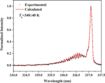
Figure 5. Experimentally obtained spectrum of the N2(C-B, 0-0) transition for the helium discharge at an applied voltage of 6 kV compared with simulated spectrum in Specair. The best fit yields a gas temperature of 340 ± 40 K. The spectrum is recorded at 58 ns.
Download figure:
Standard image High-resolution imageThe temporal evolutions of the electron density in pure helium discharge during the initial stage for different applied voltages are shown in figure 6. Note that all the earliest data points in time regarding spectroscopic measurements yield information about moments in time after the observation of the hollow structure because of both weak light emission of the hollow profile and jitter of the voltage pulse with respect to the camera gate. After breakdown, the discharge power increases (see figure 4) corresponding to an increase of electron density in excess of 1021 m−3 as shown in figure 6(b). The delay in the increase of the electron density decreases with increasing applied voltage, consistent with the decrease of the current rise. After the initial peak in power, the emission intensity becomes weak making it difficult to measure electron densities at longer times. In spite of the large difference in discharge power, the maximum electron density remains about 2.6−3 × 10²¹ m−3 for the applied voltage varying from 3 to 6 kV. The increase in spark radius with increasing voltage and energy dissipation allows for this constant electron density. The lowest electron density that can be accurately measured using the Stark spectroscopy of the He I at 492.19 nm considering the uncertainty of different broadening mechanisms (electric field induced Stark effect included) is 1021 m−3, which is similar to the reported lower values.
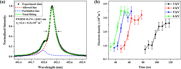
Figure 6. (a) Line profile of the Voigt fit of the allowed and forbidden component of He I line for 6 kV at 43 ns (no polarizer in the optical path). (b) Time-evolution of electron density during ignition stage of helium discharge for different applied voltages.
Download figure:
Standard image High-resolution imageThe vertical electric field in the center of the electrode gap at the initial stage of the discharge is measured by the intensity ratio of the π-components of the allowed and forbidden lines at 492.2 nm. The emission intensity increases with the increasing power while the line width becomes broader making the line profiles of the allowed and forbidden transitions overlap considerably. Therefore, we could only extract values of the electric field strengths during the onset of the discharge emission. The π-polarized line profiles of the He I 492 nm line for 3 and 5 kV with the fit of the forbidden and allowed components are shown in figure 7. The vertical components of the electric field at the center of the gap for applied voltages of 3 and 5 kV are evaluated to be 5.8 ± 0.4 (E/N ∼ 24 Td) and 8.2 ± 0.2 kV cm−1 (E/N ∼ 33 Td) at 98 and 43 ns, respectively. The minimum DC breakdown electric field in helium at atmospheric pressure is about 4.0 kV cm−1 corresponding to the reduced electric field of 18.6 Td. The experimentally determined electric field values are thus consistent with discharge generation with an overvoltage. The obtained electric field will be an underestimate of the electric field during the presence of the hollow profile as most of the emission will originate after the hollow profile. The reduced electric field of the discharge at 5 kV is significantly higher than the electric field of the discharge at 3 kV. Indeed, the appearance of the hollow structure seems to be correlated with high electric field. As the hollow structure also occurs at the initial stage of the discharge, it is useful to compare the result with the Laplacian electric field obtained by an electrostatic 2D simulation for the discharge geometry using Comsol Multiphysics 5.3 software. The mesh generated by the Comsol Multiphysics software was made of triangular elements of 5 μm maximum size with a 2.5 curvature factor. The simulation result is shown in figure 8 for an applied voltage of 6 kV. The contour profile of the Laplacian electric field looks very similar to the hollow structure of the emission intensity. The transition to the hollow structure starts to appear at an applied voltage between 4 and 5 kV corresponding to a Laplacian reduced electric field between 28 and 35 Td. These values of the Laplacian electric field are similar but indeed slightly higher than the measured electric fields.
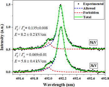
Figure 7. π-polarized emission spectra of the allowed (1s2p1P1–1s4d1D2) and forbidden (1s2p1P1–1s4f1F3) components of the He I 492 nm lines. The applied voltage of the discharge is 3 and 5 kV obtained at 93 and 43 ns, respectively.
Download figure:
Standard image High-resolution image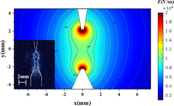
Figure 8. Laplacian electric field distribution of the pin-to-pin structure for an applied voltage of 6 kV.
Download figure:
Standard image High-resolution imageThe appearance of the hollow structure can be caused by three different mechanisms:
- (1)Disturbance of electric field by remaining space charge from the previous pulse. It is possible as in [53] that the subsequent discharge avoids the location of the first discharge and could be even hugging the previous plasma channels as found in N2, air and Ar. However this phenomenon is strongly dependent on both the time delay between the pulses (from tens of microseconds to hundreds of microseconds in argon and air) and on the discharge gas. In the present study, the phenomenon was observed for Δt between two discharge events from 1 ms to 5 s, time scales which are much longer than in [53]. This suggests that the mechanism found in [53] is not consistent with the hollow structure found in this work.
- (2)Absorption of emission in an optically thick plasma. Since the phenomenon occurs early in time at the first visible emission before a significant increase in electron density is observed, the optically thick plasma is highly unlikely and most likely would last longer than the observed hollow profile phenomenon.
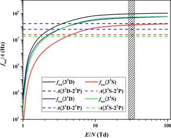
- (3)Fast depopulation of the excited states responsible for the emission in the discharge. We observed experimentally (data not shown) that the dominant emission intensity of the helium nanosecond pulsed discharges in the visible spectrum originates from the atomic helium lines at the wavelength of 587.56, 706.52, 667.82 and 728.13 nm, corresponding to the 33D, 33S, 31D and 31S excited helium states. The dark region at the center of the two pins for higher applied voltages during the breakdown must coincide with a reduced density of these excited states. The depopulation of the above radiative states could be by electron-impact stepwise excitation and/or ionization. In order for excitation/ionization to dominate over radiation, the frequency of stepwise excitation/ionization in higher electric field should be much higher than the spontaneous emission rate. To verify our hypothesis, we calculated the rate of stepwise excitation/ionization obtained from the Boltzmann solver Bolsig+ [54], using the electron-impact excitation and ionization cross section databases for the He ground state and the stepwise excitation cross sections for the excited states reported in [55, 56]. Other required parameters such as the gas temperature and the electron density are taken from the measurements. The ratios of the densities of metastable and excited states of helium to its ground state are assumed to be on the order of 10−5 and 10−6 [30]. It was verified that the calculation results for E/N > 10 Td are not very sensitive to these values. The stepwise ionization frequencies fion of the above reported helium excited states as a function of the reduced electric field E/N are shown in figure 9. When the reduced electric field reaches a value between 28 and 35 Td corresponding to the transition of the hollow structure as indicated by the dashed area in figure 9, the excitation frequencies are at least five times larger than the radiative rate. It means that the loss of the excited states by stepwise excitation and ionization becomes dominant in the range where the hollow structure appears and hence inhibits spontaneous emission. The origin of the sharp edges of the hollow structure remains however unclear and space charge effects cannot be excluded. More detailed explanations will require complementary computational efforts which are outside the scope of this work.
Figure 9. Ionization frequency for helium excited states (33D, 31D, 33S and 31S) as a function of the reduced electric field compared to the Einstein coefficient of the four excited states responsible for the dominant emission lines between 300 and 800 nm. The dashed area represents an E/N between 28 and 35 Td corresponding to the Laplacian field calculated for an applied voltage of 4 and 5 kV, respectively.
Download figure:
Standard image High-resolution image
4. Conclusion
In the paper, the initial stage of pin–pin nanosecond pulsed discharges at atmospheric pressure was investigated in different gases (helium, humid helium, argon and air). In all the investigated gases a hollow structure is observed at the initial stage of the discharge. The reported results show that a threshold voltage is required for the appearance of a hollow profile and the effect is observed in all investigated gases.
Measurements of the axial electric field using Stark polarization spectroscopy show that the helium discharges are generated by an overvoltage pulse since the measured fields are much higher than the DC breakdown field of helium at atmospheric pressure. Moreover, the increase in electric field amplitude corresponding with the increase in applied voltage correlates with the formation of hollow structures. This is further supported by the observation that the hollow profile resembles equipotential electric field lines from the corresponding 2D Laplacian field. The hollow structure phenomenon was found not to be very sensitive to the time delay between voltage pulses suggesting that collisional depopulation of the excited states could be involved. However detailed modeling studies of the phenomenon are required to validate this hypothesis [42].
Acknowledgments
The authors would like to acknowledge funding provided by the Department of Energy, office of Fusion Energy Science grant through the general Plasma Science Program (AT4010100) and the University of Minnesota. Chuan-Jie acknowledges the Chinese Scholarship Council for the fellowship (No. 201706060142) to support his research stay at the University of Minnesota.