
Abstract
Objective. Microbeam radiation therapy (MRT) is an alternative emerging radiotherapy treatment modality which has demonstrated effective radioresistant tumour control while sparing surrounding healthy tissue in preclinical trials. This apparent selectivity is achieved through MRT combining ultra-high dose rates with micron-scale spatial fractionation of the delivered x-ray treatment field. Quality assurance dosimetry for MRT must therefore overcome a significant challenge, as detectors require both a high dynamic range and a high spatial resolution to perform accurately. Approach. In this work, a series of radiation hard a-Si:H diodes, with different thicknesses and carrier selective contact configurations, have been characterised for x-ray dosimetry and real-time beam monitoring applications in extremely high flux beamlines utilised for MRT at the Australian Synchrotron. Results. These devices displayed superior radiation hardness under constant high dose-rate irradiations on the order of 6000 Gy s−1, with a variation in response of 10% over a delivered dose range of approximately 600 kGy. Dose linearity of each detector to x-rays with a peak energy of 117 keV is reported, with sensitivities ranging from (2.74 ± 0.02) nC/Gy to (4.96 ± 0.02) nC/Gy. For detectors with 0.8 μm thick active a-Si:H layer, their operation in an edge-on orientation allows for the reconstruction of micron-size beam profiles (microbeams). The microbeams, with a nominal full-width-half-max of 50 μm and a peak-to-peak separation of 400 μm, were reconstructed with extreme accuracy. The full-width-half-max was observed as 55 ± 1 μm. Evaluation of the peak-to-valley dose ratio and dose-rate dependence of the devices, as well as an x-ray induced charge (XBIC) map of a single pixel is also reported. Significance. These devices based on novel a-Si:H technology possess a unique combination of accurate dosimetric performance and radiation resistance, making them an ideal candidate for x-ray dosimetry in high dose-rate environments such as FLASH and MRT.
Export citation and abstract BibTeX RIS

Original content from this work may be used under the terms of the Creative Commons Attribution 4.0 licence. Any further distribution of this work must maintain attribution to the author(s) and the title of the work, journal citation and DOI.
1. Introduction
The generation of ultra-high dose-rate x-rays at synchrotron facilities is extremely attractive as an alternative radiotherapy treatment modality for incurable tumours. Known as the 'FLASH' effect, the exposure of tumour tissue to dose rates on the order or above 40 Gy s−1 has been reported to result in less damage to surrounding normal tissues whilst maintaining tumour control similar to that seen in conventional radiotherapy techniques that deliver a dose rate of 6 Gy min−1 (Wilson et al 2020, Posar et al 2021). Additionally, the collimation of high dose-rate synchrotron beams into multiple micron-sized beams (known as microbeam radiation therapy or MRT) has demonstrated promising results in animal-based studies with improved effectiveness on tumour control (Laissue et al 1998, Bräuer-Krisch et al 2010, Bouchet et al 2013, Engels et al 2020). As the development of MRT moves towards clinical applications (Grotzer et al 2015, Adam et al 2022), devices that can accurately monitor dose deposited prior to and during treatment, offering capabilities to resolve the profile of microbeams with high spatial resolution are vital. The quantities of interest for quality assurance (QA) in MRT are the full-width half-maximum (FWHM) and the centre-to-centre (c-t-c) spacing of the fractionated microbeams, as well as quantifying the ratio of the dose deposited by the microbeam peaks to the dose in the valley regions between peaks, also known as the peak to valley dose ratio (PVDR).
Providing accurate dosimetry for MRT is challenging as detectors need to have micron-scale spatial resolution, a wide dynamic range to cope with the extremely high dose rates and provide accurate dosimetry under soft x-ray irradiation conditions. At the ANSTO Australian Synchrotron (AS), light for MRT is generated with a continuous spectral distribution with average energy ranging from 60 to 120 keV (Livingstone et al 2016), depending on the beam filtration option selected. Commercial devices such as ionisation chambers (ICs) routinely used in clinical radiotherapy can operate accurately at ultra-high dose rates with appropriate correction factors (Fournier Crosbie et al 2016), but lack the spatial resolution required to resolve individual microbeams. Radiochromic films are also commonly used in FLASH and MRT dosimetry as they can accurately measure microbeam widths and separations (Pellicioli et al 2019). However, the shortcomings of film-based dosimeters include lack of real-time response, the requirement of two different films to quantify PVDR (one sensitive to the high peak doses and one sensitive to the low valley doses), and spatial resolution limited by the granularity of the films and polymer diffusion after irradiation (Crosbie et al 2008). Organic photodiodes (OPDs) have demonstrated extremely promising results in MRT dosimetry applications, demonstrating excellent spatial resolution, tissue-equivalence, and radiation hardness up to 40 kGy (Posar et al 2020). The shortfall of OPDs arises from their requirement of encapsulation due to material instability in air (Logothetidis et al 2010), with encapsulation materials (often Polyethylene-based) observed to generate artificial satellite peaks when attempting to resolve individual microbeams (Posar et al 2021). Dosimeters employing micron-sized plastic scintillators with optical-fibres have also been investigated in the work of Archer et al (2018), resulting in accurate real-time dosimetry of synchrotron microbeams with a 10 μm thick sensitive volume. However, the energy dependence of the combination of fibre-optic and OPD dosimeters are heavily dependent on the plastic scintillator material used (Archer et al 2018, Posar et al 2020, Large Posar et al 2021). Silicon strip detectors are an attractive solution for MRT dosimetry, with spatial resolution able to resolve individual microbeams and dosimetric response closely matching commercially available detectors (Lerch et al 2011, Wong et al 2011, Petasecca et al 2012, Fournier et al 2016, Davis et al 2022). A promising solution for MRT dosimetry is also represented by single-crystal diamond dosimeters such as the commercially available PTW microDiamond 60019, which has demonstrated exceptional performances for dosimetry of synchrotron microbeams. This detector has the greatest one-dimensional spatial resolution (1 μm) and has demonstrated accurate and reliable microbeam measurements (Livingstone et al 2016, Livingstone et al 2018, Davis et al 2019). However, alignment remains a difficult and time-consuming step as the large aspect ratio of the PTW microDiamond's cylindrical sensitive volume (1 μm thick and 2 mm diameter) can result in significant impacts on measurement of the synchrotron microbeams from even slight misalignments. Moreover, the PTW microDiamond detector is designed for operation in conventional MV radiotherapy, and so the energy dependence and limited radiation lifetime in ultra-high dose rate environments must be considered for its application in MRT dosimetry.
This work explores the possibility to combine the advantages of silicon detectors (with proved fabrication stability and limited cost) with the advantage of diamond devices with their micron-scaled sensitive volume. This combination is possible using Hydrogenated amorphous silicon, or a-Si:H. This material, historically developed for energy harvesting by the solar-panel industry, has been investigated for direct ionising radiation detection using a planar diode architecture. An advantageous feature of a-Si:H is its superior radiation hardness, with Wyrsch et al (2006) reporting an increase in the leakage current of a 32.6 μm a-Si:H p-i-n diode of only a factor of 2 when held at a 9 × 10⁴ V cm−1 electric field and irradiated with 24 GeV protons up to a fluence of 7 × 10¹⁵ p cm−2. Furthermore, the radiation hardness and sensitivity of a-Si:H devices exposed to gamma irradiation has been reported (Boudry and Antonuk 1994, Kim et al 2002, Menichelli et al 2021). Detailed motivations behind the use of a-Si:H diodes for beam monitoring and dosimetry in high-dose environments is presented in full in Menichelli et al (2020). The structure of ionising radiation detectors based on a-Si:H may be in the p-intrinsic-n (p–i–n) or in the Schottky junction forms. The intrinsic a-Si:H layers used in both p–i–n and Schottky devices are produced via plasma enhanced chemical vapour deposition (PECVD) of a mixture of Silane gas (SiH4) and molecular hydrogen at temperatures of up to 250 °C (Shah et al 1992). The introduction of hydrogen gas during PECVD is optional, as the hydrogen content in the Silane will still provide hydrogenation of the amorphous silicon. However, the addition of H2 gas alongside Silane during PECVD has been previously observed to improve both material and device qualities (Guha et al 2003). The resulting material is a disordered semiconductor with short-range order. In a-Si, the absence of long-range order gives rise to broken or unsatisfied Si–Si bonds resulting in tail states from both the conduction and valence bands, which extend into the band gap (Klaver 2007). For a-Si:H, the introduction of hydrogen (at least 4%–10% atomic) passivates the effect of most of the dangling bonds, reducing the defect density within the amorphous silicon structure and reducing recombination cross sections. The lowered defect concentration also enables the deposition of doped regions (Street 2005). In alternative to p–i–n structures, a-Si:H devices can be fabricated using dopant-free carrier selective contacts (CSC). Both electron and hole CSCs were recently successfully developed at École Polytechnic Fédérale Lausanne (EPFL) for c-Si and a-Si:H solar cell devices. These include materials such as MoOx , WOx , TiOx or LiF, that can be often deposited by atomic layer deposition (Bivour et al 2015). Deposition of a-Si:H via PECVD allows for the fabrication of a-Si:H devices over large areas at low cost with high reproducibility. Furthermore, PECVD of a-Si:H can be performed on a wide variety of substrates including flexible materials such as polyimide (Kapton©), polyethylene naphthalate (PEN) and polyethylene terephthalate.
The experimental dosimetric characterisations summarised in this work are performed on an innovative a-Si:H device structure based on a selection of CSC deposited on an intrinsic amorphous substrate (Menichelli et al 2021). The dosimetry protocols adopted are the ones developed for synchrotron-based radiotherapy and MRT as outlined in the works of Prezado et al (2011) and Davis et al (2022).
2. Methodology
2.1. Detector architecture and assembly
The a-Si:H detectors were fabricated at the photovoltaics laboratory of EPFL, located in Neuchâtel, Switzerland. The detectors can be described as planar barrier diodes with electron selective contacts on one side and hole selective contacts on the other side. The electron selective contact is formed through the deposition of either ZnO:Al (AZO) or TiO2 on glass via sputtering with thicknesses of 60 nm or 10 nm, respectively. The active a-Si:H detector layer is intrinsic (undoped) and deposited via PECVD at selected thicknesses of 0.8 and 6.2 μm. The hole selective contacts on the top of the device were fabricated via sputtering with a 20 nm thick MoOx layer and protected by 60 nm of indium titanium oxide (ITO). Each device contains 4 pixels with an area of 4 × 4 mm2. The devices are mounted on polyimide (Kapton) tails and readout in real-time using a custom-designed, multichannel electrometer developed by the Centre for Medical Radiation Physics (CMRP) at the University of Wollongong, Australia (Fuduli et al 2014). Each pixel of the a-Si:H devices are connected to gold contact pads on the Kapton PCB tails via thin copper wires (50 μm diameter) bonded with silver paint and epoxy to the a-Si:H detector ITO top contacts (see figure 1(b)). The detector architecture is illustrated in figure 1(a).

Figure 1. (a) Architecture of the a-Si:H planar diode structures employed in this study, the top hole selective contact is comprised of MoOx and has a protective ITO layer on top, while the bottom electron selective contact can be AZO or alternatively TiO2. (b) Fabricated device as assembled on the Kapton tail for electronic read-out. Visible here are the thin copper wires attached to the diode top contacts using conductive silver paint and epoxy.
Download figure:
Standard image High-resolution imageA preliminary characterisation of the electrical behaviour and sensitivity of these devices irradiated by x-rays from a 50 kV, 200 μA x-ray tube with a 125 μm Be window are presented by Menichelli et al (2022).
2.2. Synchrotron beamline and reference dosimetry
Experimental measurements were performed at the Imaging and Medical Beamline (IMBL) of the ANSTO Australian Synchrotron. The IMBL x-ray beam is extracted from the electron storage ring (3 GeV, 200 mA) by a superconducting multipole wiggler with operating magnetic field strengths between 1.4 T and 4.2 T. In this study, the beam is configured with a 4 T wiggler field to maximise the beam intensity. All experiments were conducted ex-vacuo on the dynamic MRT stage (DynMRT) in hutch 2B of the IMBL, with the beam window located 32 m downstream of the wiggler magnet. Filtration and hardening of the beam are controlled via five in vacuo filter paddles, located upstream of hutch 2B. Paddles 1 to 3 are left in the standard configuration (paddle 1 = 14.14 mm high-density Carbon, paddle 2 = 0.64 mm Carbon, paddle 3 = 0.35 mm). For paddles 4 and 5, different combinations of metallic foils can be selected by the user to alter the energy profile and dose rate of the extracted synchrotron beam. In this paper, three alternative filter configurations are adopted, with the selected filter combinations and their impact on the delivered beam summarised in table 1. Such a configuration at the IMBL beamline is referred to as 'pink' beam settings due to the polychromatic x-ray beam resulting from the filtration. The extracted beam traverses along the defined x-axis of the beamline and is shaped via a conformal mask to produce a 20 × 20 mm2 field in the Y–Z plane. A beam-defining aperture (BDA) further controls the height of the beam (in the Z direction), with heights ranging from 0.5 to 2 mm. A complete description of the IMBL, including beamline components, the adopted coordinate system and delivered energy spectra, are given in the works of Hausermann et al (2010), Stevenson et al (2017) and Livingstone et al (2018), respectively. The beam with 0.5–2 mm height and a width of 20 mm (in the Y direction) is referred to as 'broad beam', in contrast to the 'microbeam' modality where an additional multi-slit collimator (MSC) is placed in the beam between the BDA and the target device or object under study.
Table 1. Beam properties as measured with PTW Type 31022 PinPoint chamber exposed to 4T 'pink' beam with 2 mm BDA and 20 × 20 mm2 field (measured at 10 mm s−1 scan speed). Uncertainties in the dose rates are calculated from compounding uncertainties in the calibration factor and recorded current of the PinPoint chamber.
| Beam filtration | Peak energy (keV) a | Dose rate (Gy s−1)—15 mm b | Dose rate (Gy s−1)—37 mm b |
|---|---|---|---|
| Al–Al | 47.8 | 6963 ± 258 | 5041 ± 188 |
| Cu–Cu | 87.5 | 702 ± 26 | 523 ± 19 |
| Mo–Mo c | 117 | 128 ± 5 | 93 ± 3 |
a Peak energies taken from Livingstone et al (2018). b Nominal depths in water-equivalent plastic during irradiations. c Short-hand for filtration paddles 4 and 5 with an Al-Mo alloy selected.
Dose calibration measurements were performed in broad beam, using the commercially available PTW (Freiburg, Germany) type 31022 PinPoint IC, with a 0.016 cm3 cylindrical sensitive volume (radius 1.45 mm, length 2.9 mm). The response of the PinPoint IC was corrected to account for pressure, temperature, and polarisation conditions during measurements. For the reference dose rate measurements presented in table 1, the IC was placed at two selected reference depths in a water-equivalent plastic phantom (solid water) with approximately 60 mm of backscatter. The reference depths of 15 mm and 37 mm were selected as devices were placed at these depths during radiation damage measurements. The IC has been calibrated by PTW with a TH 200 x-ray beam (109 keV mean energy), allowing for the accumulated charge to be used to calculate the absorbed dose to water. This reference data is used to calculate the absorbed dose to water at the two reference depths for a variety of beam filtrations and deliveries. As a result, the response of the a-Si:H detectors under identical conditions can be converted to absorbed dose and expressed in the SI unit of Grey (Gy).
2.3. Detector phantom and beamline set-up
All experiments were conducted on the DynMRT stage in Hutch 2B of the IMBL. Measurements were performed with set at various depths within a water-equivalent plastic phantom, custom fabricated for each detector to minimise air gaps. The result allows for the direct comparison between the absorbed dose to water as estimated by the reference measurements and the delivered dose to the detectors.
To take advantage of the micron-scale sensitive volume of the a-Si:H detectors, an 'edge-on' orientation can be adopted for high spatial resolution dosimetry. In contrast to a 'face-on' orientation where the beam is incident normal to the surface of the detector, the 'edge-on' modality situates the detector such that the surface of the detector is oriented parallel to the direction of the beam. As a result, the spatial resolution of the detector is defined by the active layer thickness. An illustration of the two detector orientations utilised in this study are provided in figure 2(b).
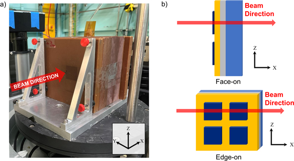
Figure 2. (a) Detector as positioned within the water-equivalent plastic phantom and mounted on the DynMRT stage of hutch 2B. (b) Illustration of the detector in face-on and edge-on orientations.
Download figure:
Standard image High-resolution image3. Results and discussion
3.1. Radiation damage
The effects of radiation damage were investigated on the 6.2 μm thick a-Si:H detector with AZO electron selective contact. The detector was placed at a depth of 37 mm in solid water with 40 mm of backscatter material. Incremental irradiation steps were performed using the 4T Al–Al 'pink' beam modality of the IMBL in broad beam conditions with a 20 × 20 mm2 field and 2 mm BDA, producing the highest dose rate available at the IMBL. A total ionising dose of over 700 kGy was delivered in increments of 20–150 kGy. Such large dose increments were delivered via repeated 10 mm s−1 vertical scans of the 2 × 20 mm2 field, delivering approximately 1 kGy per scan. The device was held at a 3 V reverse bias during irradiations. After each irradiation step, the response of the detector at 3 V reverse bias to three 10 mm s−1 vertical scans with Mo–Mo filtration (lowest dose rate) was recorded, measuring integral response and variation of the baseline (corresponding to the dark current) as a function of total ionising dose (TID). The response and associated error bars were calculated as the average and one standard deviation of the three Mo–Mo scans between each irradiation step, delivering approximately 20 Gy per scan.
In figure 3(a), the initial response of the a-Si:H detector structure is observed to decrease rapidly with increasing TID. Between 0 and 175 kGy, the integral response of the device to the reference 4T Mo–Mo scans degraded by 24% from 153 to 116 nC. Above 175 kGy, this variation is reduced to within 19%, with a difference in integral charge collected for TIDs of 175 and 700 kGy of less than 6.5%. This suggests that past 175 kGy the radiation effects within a-Si:H stabilise and the detector can be used reliably for high dose-rate applications such as MRT.

Figure 3. (a) Integral response and (b) leakage current of a-Si:H as a function of total ionising dose. Between points I and II labelled on each figure, there was a 1 h break in irradiations. Error bars are calculated as one standard deviation. Error bars in (a) are smaller than the marker. The large error bars in (b) are due to the electronic noise being of comparable signal strength to the detector leakage current.
Download figure:
Standard image High-resolution imageThe value of 19% degradation in the TID range of 175–700 kGy refers to the large drop observed in response seen between points I and II in figure 3(a). Due to the extremely high dose rates delivered to the detector from repeated scans through the 4T Al–Al synchrotron broad beam (5 kGy s−1—table 1), a large amount of heat was generated in both the sample and the water-equivalent plastic phantom. Between points I and II in figure 3(a), irradiations were halted for 1 h. This break in irradiations allowed for adequate cooling of the sample and, as a result, a large reduction in the response of the device. As irradiations re-commenced and the sample approached the same temperature equilibrium reached at point I, the integral response increases back to within 6.5% of its pre-break value.
Figure 2(b) investigates the relationship between the device leakage current and TID. Between 0 and 290 kGy (point I), the leakage current was observed to increase linearity at a rate of (2.62 ± 0.18) fC/kGy. Following the break in irradiations, the leakage current again increased linearly at a comparable rate of (2.82 ± 0.07) fC/kGy between 380 kGy (point II) and 700 kGy. Hence, this cooling or annealing effect is also reflected in the leakage current of the device, with figure 2(b) displaying a drop in leakage current between points I and II. Further study on annealing effects in a-Si:H should be undertaken to investigate the effects of recovery and stabilisation of the response after heavy irradiation by x-rays. To allow for a more controlled assessment of radiation-induced damages in a-Si:H devices, future measurements should adopt a lower dose rate to ensure thermal stabilisation of the samples and heat-induced sample damage is minimised. Future depth-dose measurements conducted in a water tank phantom would also reduce sample heating effects.
As identified previously, the studies of Wyrsch et al (2006) and Menichelli et al (2022) are pivotal studies in documenting the radiation resistance of a-Si:H to high fluence proton and neutron irradiations, respectively. Whilst these studies display the intrinsic radiation hardness of a-Si:H, they are more related to applications of a-Si:H for particle detection. Concerning applications in x-ray dosimetry, Boudry and Antonuk (1994) report x-ray induced damages of a 1 μm thick n–i–p a-Si:H diode structure, irradiated up to a total dose of ∼3 kGy via a 60Co source. They observe an initial region of negligible change in the leakage current of their device up to a TID of approximately 1 kGy. After this point, a linear increase in leakage current is observed at rates of between 0.7 and 3.8 pA/Gy, a result comparable with the ones obtained in this study. Kim et al (2002) performed a similar study via 60Co irradiations incident on a series of n–i–p a-Si:H diodes to a much higher TID of approximately 40 kGy. These diodes also possessed intrinsic layer thicknesses of 1 μm. They observe a linear increase in device leakage currents between 0 and 40 kGy, at a rate of 0.06–0.07 A mm−2 kGy−1 (depending on the device architecture).
In clinical applications of a-Si:H detectors for dosimetry and in-line beam monitoring during MRT, successive high dose-rate irradiations of targets using the 4T Al–Al modality of the IMBL would never occur. Furthermore, these results demonstrate the detector can be used repeatedly for MRT QA measurements with minimal degradation in performance or requirement of frequent calibrations. Hence, the radiation damage measurements performed in this study at the AS align closely with the results in the literature whilst also providing an assessment of radiation hardness in a-Si:H at a far higher TID than reported previously.
This reported radiation resistance in a-Si:H devices is essential for not only repeated QA dosimetry measurements under the high dose-rates of MRT and FLASH radiotherapies, but also for measurements whereby the detector is subject to extended or continual irradiations. A prime example of such an application is in-line beam flux monitoring where the detector is placed in the periphery of the beam.
3.2. Broad-beam dosimetry
3.2.1. Dose linearity and sensitivity
Figure 4 displays the dose linearity of the four a-Si:H device variations exposed to the 4T-MoMo modality of the synchrotron broad beam. The devices were placed at a depth of 37 mm in solid water with 40 mm of backscatter material. The detectors were placed in a face-on orientation and scanned vertically (along the Z axis) through the centre of the 20 × 20 mm2 homogenous irradiation field using the 2 mm BDA. The dose delivered was modulated by selecting scan speeds of 5, 10 and 20 mm s−1, corresponding to delivered doses (in water) of 40, 20 and 10 Gy, respectively. Dose linearity was measured for all devices operated passively (0 V) and under reverse bias (1 V for 0.8 μm, 3 V for 6.2 μm). The response of the device at each dose point was calculated as the average integral charge (above background) received over all 4 pixels of the device from the 3 repeated scans. The associated error bars represent one standard error between pixels. Uncertainties in the delivered dose due to scan speed uncertainties are on the order of 0.05%, hence horizontal error bars are contained within the size of the marker. The sensitivity of each device, calculated from the gradients in figure 4, are presented in table 2.
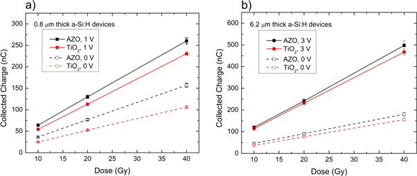
Figure 4. Dose linearities at 0 V and under reverse bias conditions for devices with (a) 0.8 μm and (b) 6.2 μm a-Si:H active layers exposed to the 4T Mo–Mo x-ray field modality of the IMBL. Error bars reflect one standard error in the response between all 4 pixels on each device.
Download figure:
Standard image High-resolution imageTable 2. Calculated device sensitivities under passive and reverse bias operation for the 4T Mo–Mo synchrotron broad beam. Sensitivities are an average over all 4 pixels of each device, and uncertainties given as the standard deviation between pixels.
| Electron selective contact material | a-Si:H layer thickness | Sensitivity at 0V (nC/Gy) | Sensitivity under reverse bias a (nC/Gy) |
|---|---|---|---|
| TiO2 | 0.8 μm | 2.73 ± 0.19 | 5.86 ± 0.32 |
| 6.2 μm | 3.97 ± 0.43 | 11.9 ± 1.3 | |
| AZO | 0.8 μm | 4.03 ± 0.46 | 6.57 ± 0.74 |
| 6.2 μm | 4.49 ± 0.83 | 12.2 ± 2.2 |
a Bias of +1 V and +3 V applied to the electron selective contact for 0.8 μm and 6.2 μm thick devices, respectively.
Excellent dose linearities (R2 > 0.999) are observed for all device thickness and electron selective contact material combinations, under both passive and reversed bias operations. The calculated sensitivities to the 4T Mo–Mo broad beam of the IMBL range from (2.73 ± 0.19) nC/Gy for the 0.8 μm thick TiO2 selective contact variant under 0 V bias to (12.2 ± 2.2) nC/Gy for the 6.2 μm AZO variant under 3 V reverse bias. The results in table 2 suggest devices with AZO electron selective contacts possess a better charge extraction than their TiO2 counterparts, resulting in higher sensitivities. For example, 6.2 μm thick devices operated passively (0 V bias) return sensitivities of (3.97 ± 0.43) nC/Gy and (4.49 ± 0.83) nC/Gy for TiO2 and AZO electron selective contacts, respectively. This increased sensitivity in AZO devices can also be attributed to the larger effective atomic number (Zeff ) of AZO compared to TiO2, resulting in more charge being generated immediately under the contact. Using the formula for Zeff in heterogeneous material by MURTY (1965) and the estimated stoichiometry for the AZO and TiO2 CSC material layers, it was calculated that Zeff (AZO) = 27.6 and Zeff (TiO2) = 18.5.
Devices with TiO2 selective contact appear to benefit from biased operation to a greater degree than AZO devices due to their higher work function and resistivity (Sittinger et al 2008). For the 6.2 μm thick devices, an increase in sensitivity by a factor of 3 is observed in the TiO2 variant compared to a factor of 2.72 observed in the AZO variant. With a variation of less than 10%, TiO2 devices also present a higher stability and reproducibility of the response between different pixels fabricated in the same substrate, in contrast to AZO devices which show a variation as large as 18% under bias conditions.
3.2.2. Percentage depth dose (PDD)
PDD or depth-dose profiles for the four a-Si:H devices were recorded for the 4T Mo–Mo filtration of the IMBL for a 20 × 20 mm2 field with 2 mm BDA. The depth of each detector in solid water was varied from 15 to 60 mm from the phantom's surface. At each depth, three vertical scans through the centre of the synchrotron's broad beam x-ray field were performed at a scan speed of 20 mm s−1. The response of each detector was calculated as the average integrated charge (above background) collected over the repeated scans at each depth, with error bars representing one standard deviation. The resulting PDD profiles are benchmarked against PDD measurements from Livingstone et al (2018) performed at IMBL under similar irradiation conditions using a cross-calibrated PTW microDiamond 60019 detector. All measurements are normalised relative to the response recorded at a depth of 20 mm, the common reference depth for broad beam dosimetry measurements performed at IMBL (Livingstone et al 2018, Posar et al 2020, Davis et al 2022).
Figure 5(a) shows an excellent agreement between all four a-Si:H detector variations and the commercially available PTW microDiamond data as recorded by Livingstone et al (2018) even using the devices in photovoltaic mode (bias at 0 V). The PTW microDiamond detector is considered energy independent for this beam spectrum delivered at IMBL (Davis et al 2019), thus benchmarking results against the microDiamond detector provides insights into the tissue-equivalence of these detectors. As seen in the lower half of figure 5(a), the percentage difference is negligible for shallow detector depths in water-equivalent plastic. The maximum variation between the a-Si:H detectors and the PTW microDiamond detector is 11.2%, recorded for the 0.8 μm thick AZO detector variant at a depth of 60 mm. All other data points in figure 5(a) return a percentage difference within ±8%. The application of bias acts to further improve the PDD response of the a-Si:H detectors (figure 5(b)), with percentage differences at all depths within ±5% of the PTW microDiamond detector. To provide further insight into the accuracy of the PDD curves recorded, the theoretical PDD curve of IMBLs 4T Mo–Mo beam in water was calculated using a custom Geant4 (Agostinelli et al 2003, Allison et al 2006) application. This simulation was run in Geant4 v11.0.1 (released March 2022) using a combination of the QGSP_BIC_HP and G4EmStandardPhysics_option4 physics lists; recommended as the most accurate physics lists for medical dosimetry and radiation protectionbased simulations (Arce et al 2021).

Figure 5. Depth-dose profiles for a-Si:H detector structures operated under (a) 0 V and (b) reverse bias conditions. For biased results in (b), 0.8 μm detectors are operated at 1 V reverse bias and 6.2 μm detectors at 3 V. The subplots in both figures display percentage difference in the PDD response of the a-Si:H devices compared to Livingstone et al (2018) using the PTW microDiamond detector. The theoretical PDD curve for the 4T Mo–Mo beam in water was calculated in Geant4 and is included in both figures for comparison.
Download figure:
Standard image High-resolution imageThe variations observed can be attributed to the thick (∼1 mm) glass substrate on which the a-Si:H devices are deposited. The glass, particularly at large depths, attenuates the x-ray backscatter from within the water-equivalent plastic detector phantom, with a rising contribution of the attenuation of the backscattering with softening of the beam (i.e. at greater depths). Further explanation of this disagreement stems from the fact that the reference data was obtained using the 3T monochromatic modality of the synchrotron with a beam energy of 120 keV, whereas the data in this study was obtained via the IMBLs polychromatic 4T Mo–Mo 'pink' beam with a peak energy of 117 keV. This is a consequence of this work being the first to publish data on the depth dose profile of the 4T Mo–Mo x-ray beam operational mode at the ANSTO AS. However, Livingstone et al (2018) has previously demonstrated that the PDD response of the PTW μDiamond is equivalent (within uncertainty) between polychromatic and monochromatic beams with closely matching peak energies. Hence, an acceptable agreement was observed between the depth dose response of the a-Si:H and the reference PTW μDiamond data, particularly under bias where agreement is within ±5% (figure 5(b)). Nevertheless, reference measurements performed with commercially available detectors (such as the PTW IC or microDiamond) under identical conditions are needed for a complete assessment of the PDD performance of a-Si:H detectors.
3.3. Microbeam dosimetry
In hutch 2B of the IMBL, the introduction of a tungsten MSC acts to spatially fractionate the 20 × 20 mm2 broad synchrotron beam into 50 micron-sized quasi-parallel (coplanar) beams. The microbeam modality of the IMBL is advantageous for applications such as MRT, where the delivery of the treatment beam with high dose-rates and spatial fractionation directly correlates to an improved sparing of normal tissue whilst delivering a prescribed dose to a target tumour volume. For QA during MRT, it is imperative that the spatial distribution of the microbeams is quantified. In this regard, important quantities include the measurement of the FWHM and c-t-c peak spacing. The clinical advantages of MRT as a radiotherapy treatment also rely on the delivery of the treatment beam with high dose-rates and a high contrast between microbeam peaks and valleys (Engels et al 2020). Therefore, a quantity named peak-to-valley dose ratio (PVDR) has been defined and must also be accurately determined.
3.3.1. Microbeam profiling
In our experiments, the MSC is placed downstream with respect to the BDA collimator set at 0.5 mm. We adopted the 4T Cu–Cu filtration of the superconducting wiggler generated x-ray beam, leading to a linear array of coplanar beams, each with a height of 0.5 mm, and nominal FWHM and c-t-c distances of 50 μm and 400 μm respectively (Livingstone et al 2018). To reconstruct the profile of the synchrotron microbeams, the device with 0.8 μm of intrinsic a-Si:H substrate and AZO electron selective contact material was placed in an 'edge-on' orientation (figure 2(b)) at a depth of 20 mm in solid water. The AZO devices proved to have a higher charge collection efficiency which is important to measure simultaneously the peak and the valley dose. The spatial distribution of all 50 synchrotron microbeams was then reconstructed in real-time by scanning the detector laterally (along the y axis) through the centre of the fractionated field at a fixed speed. The real-time readout of the CMRP's custom-designed electrometer allows instant visualisation of the synchrotron microbeams, returning collected charge in the detector as a function of time as the detector is moved through the irradiation field. Knowing the sampling time of the electrometer and the speed at which the detector is scanned laterally across the microbeams, this real-time data can be used to convert the response of the detector as a function of time into a charge distribution as a function of distance. The resulting intrinsic microbeam field scan is depicted in figure 6.
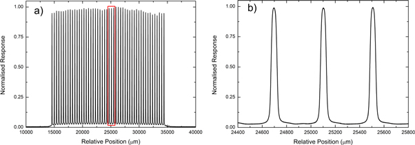
Figure 6. Response of a-Si:H detector with 0.8 μm active layer thickness and AZO electron selective contact operated in 'edge-on' mode, producing (a) spatial profile of all 50 microbeams via intrinsic scan and (b) zoomed-in image of the three central microbeams. The position of the peaks resolved in (b) is indicated by the red box in (a).
Download figure:
Standard image High-resolution imageIdeally, with minimal beam divergence and scattering, the profile of each microbeam should follow a rectangular shape with a relatively flat top and sharp edges, as has been observed with the PTW microDiamond (Livingstone et al 2016). To assess the capability of the a-Si:H detectors to replicate this result, we took advantage of the fast sampling and short integration time of our custom-designed electrometer. With an integration time of 160 μs and a lateral scan speed of 2 mm s−1, the resulting single microbeam profile is reconstructed with an effective scan resolution of 0.32 μm. Although uncertainties may arise from the scan speed of the DynMRT sample stage, previous publications have reported accurate profiling using much slower scan speeds than the 2 mm s−1 used in this instance (Archer et al 2018). Hence, uncertainty in the selected scan speed is considered negligible. The response was normalised to the maximum recorded intensity. Figure 7 shows the results of this investigation, with the profile as measured with the 0.8 μm a-Si:H detector after an accurate alignment in respect to the beam. The data show the expected rectangular microbeam shape with flattened peak and sharply dropping sides with excellent agreement with the PTW microDiamond detector (Livingstone et al 2016).
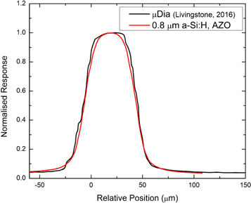
Figure 7. Close-up of a central 4T Cu–Cu microbeam profile as reconstructed fast intrinsic scan from the 0.8 μm thick a-Si:H detector with AZO selective contact in 'edge-on' modality (red trace). A microbeam profile obtained using the PTW microDiamond detector (black trace) is provided for direct comparison (taken from Livingstone et al 2016).
Download figure:
Standard image High-resolution imageAs the a-Si:H pixels possess 4 mm side-lengths, the lateral excess of the sensitive volume which is not directly in the beam will produce an additional signal due to scattered radiation. This effect may lead to some distortion in the recorded microbeam profiles. However, the reference data obtained with the PTW microDiamond detector (Livingstone et al 2016) has a diameter of 2 mm and thus is susceptible to similar scattering conditions. As a result, the comparison of the performance of the PTW microDiamond and the a-Si:H detectors of this work show excellent agreement as seen in figure 7.
3.3.2. Peak-to-valley dose ratio (PVDR)
PVDR as a function of depth between 9 and 60 mm has been measured using the 0.8 μm AZO detector placed at various depths in a water-equivalent plastic phantom. In order to measure the actual dose delivered in a realistic treatment field scenario and evaluate the corresponding treatment field PVDR, a different scan modality named Step-and-Shoot (SnS) is adopted. In SnS mode a full treatment irradiation delivery is performed and the total dose at the point of measurement recorded by the detector. The detector is then moved to the next measurement position, typically laterally by 5 microns, and the whole process repeated. The profile of the 3 central microbeams were recorded in SnS mode at each depth (figure 8(a)) and the PVDR was calculated (figure 8(b)). All measurements were conducted with the device under 0 V applied bias and exposed to 4T Cu–Cu microbeams.

Figure 8. (a) Variation in the profile of the three central 4T Cu–Cu microbeams as a function of depth in a water-equivalent plastic phantom, obtained with 0.8 μm thick, AZO selective contact a-Si:H detector operated at 0 V bias. (b) Comparison of the observed PVDR values as a function of depth obtained in this work using the a-Si:H detector at 0 V (black boxes, left axis) and the work of Livingstone et al (2018) using the PTW microDiamond detector (red circles, right axis).
Download figure:
Standard image High-resolution imageThe general trend of the PVDR as a function of depth recorded with the a-Si:H matches closely to the reference data from Livingstone et al (2018), signifying that the depth variation response of a-Si:H is consistent with the PDD for both the microbeam and broad beam modalities. However, comparing the absolute value of the PVDR measured in this work with those measured using the PTW microDiamond detector (figure 8(b)), we see a considerable under-response of a-Si:H in accurately quantifying the value of the PVDR.
The a-Si:H detector under responds by a factor of between 3.5 and 4 at all depths compared to the PTW microDiamond detector. Although figure 6 would allude to the PVDR response of the a-Si:H being much better than what is reported in figure 8, figure 6 is produced via a lateral scan of the fractionated microbeam field. This lateral scan does not record an actual dose profile of the spatially fractionated field but simply measures the intensity or beam flux. The PVDR response of a-Si:H has been measured by performing full vertical scans at each lateral position, accumulating dose from the entire beam at this position as well as from scattered radiation when the beam is above and below the sensitive volume. Estimates of the dose recorded in the microbeam peaks of figure 8(a) closely approximate the expected values, identifying that the origin of this poor PVDR response lies in the inability of the a-Si:H detectors to accurately measure the valley dose. This arises from a convolution of effects. The first is the impact of the support material on which the a-Si:H is deposited. The substrate is a high-density silica glass with a thickness of approximately 1 mm. This material has two-fold effects of attenuation of the lateral scattering (creating a slightly asymmetrical response of the sensor as can be observed in figure 8(a) and enhancing spectral energy differences between peaks and valleys. The combination of these packaging and glass support effects has been previously observed in relevant literature shown to create an asymmetric distortion in the reconstruction of the microbeam dose profiles (Rosenfeld et al 2005). The second, and perhaps most dominant cause, arises from the dose-rate dependence observed in a-Si:H detectors. Preliminary characterisations of the a-Si:H detector dose rate dependence have been performed under exposure to 6 MV x-rays generated by a Varian 2LiX clinical linear accelerator. Measurements show a strong over-response in a-Si:H at low dose-rates comparable with those experienced in microbeam valley regions. This over-response can be as large as a factor of 2.5 for dose-rates on the order of 0.5 × 10⁻⁴ Gy/pulse in respect to 2.78 × 10⁻⁴ Gy/pulse corresponding to normalisation conditions (figure 9). For further context, the recorded dose per pulse can be divided by the 3.5 μs pulse length of the 2LiX to express the x-axis of figure 9 in instantaneous dose rate. For the normalisation condition, this corresponds to an instantaneous dose rate of 77 Gy s−1. Taking into account that the peak dose rate can be as high as 5 kGy s−1, a relative factor of 3 observed between PVDR measured by a-Si:H and diamond detector is most likely due to dose rate dependence. Promisingly, devices that had undergone mild pre-irradiations to a TID on the order of 10–20 kGy and were operated under an applied reverse bias observed a dramatic reduction of this dose-rate dependence (figure 9). As a result, a-Si:H detector responses varied by less than 5% for dose-rates of around 3–4 × 10⁻⁴ Gy/pulse. Therefore, the poor performance of a-Si:H detectors in measuring PVDR can potentially be mitigated through pre-irradiation and biased operation.
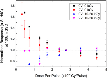
Figure 9. Dose-rate dependence of a-Si:H as measured via Dose per pulse measurements made with a-Si:H devices exposed to 6 MV photons.
Download figure:
Standard image High-resolution image3.4. Mapping and characterisation of the charge collection by x-ray beam induced charge (XBIC)
In MRT dosimetry it is important to have a detector with a well-defined sensitive volume because the presence of possible lateral diffusion currents in the substrate may create distortion during the reconstruction of the microbeams. This is a typical effect in solid state detectors such as the silicon microstrip developed by Lerch et al. which adopts a substrate with a long lifetime and, in order to limit diffusion currents, the sensitive volume must be limited by a guard ring (Lerch et al 2011).
To assess the shape and extension of the sensitive volume, XBIC is a powerful technique to map the charge collection efficiency of a sensor exposed to the same spectrum used for clinical applications. The field-size of the synchrotron beam fractionated by the MSC can be restricted such that only the central microbeam is incident on the detector surface (50 μm FWHM, 0.5 mm height). With the detector placed face-on and irradiated in air, a single 4T Cu–Cu microbeam was scanned laterally across the face of the pixel at a speed of 1 mm s−1. After each lateral scan, the detector was translated vertically in Z by 0.5 mm and the lateral scan repeated. This process was carried out until the entire surface area of a pixel has been covered. Figure 10 shows the resulting XBIC map in pC and logarithmic scale.
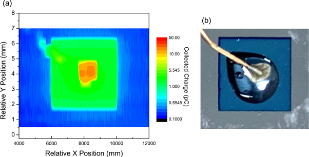
Figure 10. (a) XBIC mapping of the charge collected in logarithmic scale by a single pixel of a 6.2 μm thick a-Si:H detector with AZO electron selective contact operated at a 10 V reverse bias. (b) An optical image of the pixel mapped via XBIC.
Download figure:
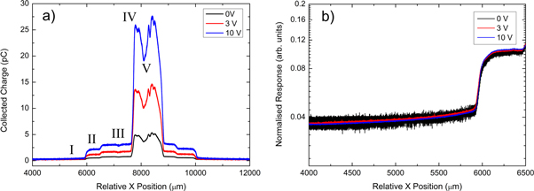
Standard image High-resolution imageNotably in figure 10, there is a localised area of increased charge collection observed in the centre of the pixel. Comparing this to the optical image of the pixel, this effect is localised where the electrical contact is made using a thin copper wire and silver-based conductive epoxy. This 'hot-spot' is attributed to a dose-enhancement caused by secondary electrons generated in the silver-based conductive paint and silver K-shell soft x-ray generated by fluorescence (approx. 22 keV). The dose-enhancement effect from the silver is undesirable when accurate dosimetry with high spatial resolution is required. This effect could also contribute directly to the discrepancies in the measured microbeam FWHM, c-t-c spacing and even PVDR values obtained in this study because it generates an asymmetric sensitivity in respect to the microbeam dose rate distribution. A closer assessment of this effect from the silver paint can be observed in figure 11, displaying the cross-sections of the charge collected as a function of the bias applied along a relative Y position of 4 mm.
Figure 11. (a) Profile of the collected charge through the centre of the pixel along a relative Y-position of 4 mm. (b) Resulting charge collection cross-sections are given for the pixel imaged in figure 10 when operated under a 0, 3 and 10 V reverse bias.
Download figure:
Standard image High-resolution image
Promisingly, the effective area of charge collection occurs only directly under the a-Si:H ITO + MoOx hole selective contact of the diode (between 6000 μm and 10 000 μm in figure 11(a)), regardless of the magnitude of the bias applied. This is visualised by the sharp drops in collected charge at the edges of the pixel in figure 11(b). This is an excellent feature for future a-Si:H device generations aiming to employ pixelated structures, as it means there will be no charge sharing between neighbouring pixels.
Figure 11(a) also shows five regions of different charge intensities as a function of lateral position. The regions are identified as:
- Baseline response of the detector;
- True a-Si:H response as the laterally scanning beam passes over the ITO + MoOx hole selective contact of the diode;
- Dose enhancement as the beam interacts with the epoxy coating of the wire contact;
- Extreme dose enhancement from K-shell electrons and fluorescence of the silver paint; and
- Attenuation of the dose-enhanced beam.
Comparing this with the optical image of the pixel in figure 10(b), we can conclude that this decrease in response is due to a combination of:
- 1.Attenuation of the Compton scattered electrons generated by the microbeam photons as they are passing through the silver and the copper wire. The copper wire also absorbs the silver florescence x-rays by before hitting the a-Si:H pixel, and;
- 2.Direct interaction of the primary x-ray beam with the packaging material leading to enhanced signal in the measured response of the detector.
These results show that packaging technology is critical in the fabrication of a dosimeter. The result of charge collection being localised to beneath the selective contact aligns with previous findings in literature for hydrogenated amorphous silicon radiation detectors. Despeisse et al (2008) observed this pixel isolation phenomenon in a 30 μm a-Si:H thin-film on ASIC (TFA) devices consisting of p–i–n a-Si:H layers on top of a CMOS circuit. Experiments conducted via electron beam induced current (EBIC) mapping of these devices displayed charge collection localised to the micron-sized pixels of this a-Si:H TFA (Despeisse et al 2008). Moreover, Franco et al (2012) further demonstrated the isolating charge collection properties of a-Si:H p–i–n diode structures, this time quantifying the behaviour for microstrip device architectures. Again using EBIC techniques, they quantified the Lateral Charge Collection (LCC) as a function of distance between neighbouring microstrips, observing a LCC region extending less than half the width of the separation distance for microstrip lateral spacings of greater than 13.4 μm (Franco et al 2012).
Although this is not a new finding for a-Si:H adopted as radiation sensor, our results show a similar behaviour under x-ray irradiation in devices employing CSCs rather than the traditional p–i–n diode architectures. Additionally, the results in figure 11 demonstrate this pixel isolation even when there is no bias applied. This is an excellent feature for future a-Si:H device generations aiming to employ pixelated structures, as it means there will be no charge sharing between neighbouring pixels even in passive mode.
4. Conclusions
The results presented in this work demonstrate the feasibility of a-Si:H diodes for applications in x-ray dosimetry and beam monitoring in ultra-high dose-rate environments, such as those utilised in FLASH radiotherapy (e.g. MRT). The devices tested have displayed excellent radiation hardness with a variation of the response of just 6.5% over a 500 kGy increase in TID. The a-Si:H diodes have proven to be reproducible in response between pixels and between measurements, low noise and linear within 0.1% up to 40 Gy total dose. The thin sensitive silicon substrate allows for a minimal energy dependence which is proved by the PDD variation in respect to the PTW microDiamond within 5% up to 60 mm depth in a solid water phantom. The structure of the a-Si:H diodes deposited on an inert substrate allows extremely thin sensitive volumes which have been demonstrated to measure the microbeams very accurately. The role of the glass support and the packaging technology adopted in this experiment has been shown to distort the reconstruction of the microbeam dose profiles, which tends to be asymmetric. This phenomenon was observed directly through an XBIC scan of a single pixel (figure 10) and through a 2D lateral scan profile from this XBIC pixel map. Dose rate dependence is also a crucial characteristic for a dosimeter used in FLASH-radiotherapy or MRT applications. In this regard, a-Si:H shows a prominent over-response at low dose rates. This effect, combined with the energy dependence created by the fluorescence of the silver-based epoxy used for the contacts, creates a strong distortion of the PVDR which is under-estimated by a factor of more than 300%. Pre-irradiation with 20 kGy allows for a mitigation of the dose rate dependence that, along with a suitable low-density material packaging of the device, should solve the problem. Further study will explore the use of a Kapton/polyimide substrate instead of the glass support wafer adopted in this study, as well as graphene-based conductive glues for the contacts.
Acknowledgments
The authors would like to thank the AS-IMBL team for the use of their facility and their assistance with the set-up and operation of the beamline. The authors would also like to thank Dr Joanna McNamara and the staff at Nowra Cancer Care Centre, Fang Su, and Ilia Filipev for their assistance in the data collection of the DPP response of a-Si:H in a clinical radiotherapy environment. This work was supported by the Australian Government Research Training Program Scholarship and the Australian Institute of Nuclear Science and Engineering Post-Graduate Research Award.
Data availability statement
The data cannot be made publicly available upon publication because no suitable repository exists for hosting data in this field of study. The data that support the findings of this study are available upon reasonable request from the authors.
Funding
The following funding is acknowledged: Australian Government Research and Training Program (RTP) scholarship to MJ Large; Australian Institute of Nuclear Science and Engineering (AINSE) Post Graduate Research Award (ALNSTU12583) to MJ Large; Programma Operativo Nazionale Ricerca e Innovazione 2014–2020 (PON R&I 2014–2022) to Francesca Peverini; Imaging and Medical Beamline at the Australian Synchrotron, Australian Nuclear Science and Technology Organisation (award No. IMBL/17499); Istituto Nazionale di Fisica Nucleare Scientific Committee (3D-SIAM and HASPIDE projects); Istituto Nazionale di Fisica Nucleare Committee for Technology Transfer (INTEF-3D-SiAm project); the Swiss National Science Foundation (grant number 200021_212208/1).