
Abstract
The imaging performance of clinical positron emission tomography (PET) systems has evolved impressively during the last ∼15 years. A main driver of these improvements has been the introduction of time-of-flight (TOF) detectors with high spatial resolution and detection efficiency, initially based on photomultiplier tubes, later silicon photomultipliers. This review aims to offer insight into the challenges encountered, solutions developed, and lessons learned during this period. Detectors based on fast, bright, inorganic scintillators form the scope of this work, as these are used in essentially all clinical TOF-PET systems today. The improvement of the coincidence resolving time (CRT) requires the optimization of the entire detection chain and a sound understanding of the physics involved facilitates this effort greatly. Therefore, the theory of scintillation detector timing is reviewed first. Once the fundamentals have been set forth, the principal detector components are discussed: the scintillator and the photosensor. The parameters that influence the CRT are examined and the history, state-of-the-art, and ongoing developments are reviewed. Finally, the interplay between these components and the optimization of the overall detector design are considered. Based on the knowledge gained to date, it appears feasible to improve the CRT from the values of 200–400 ps achieved by current state-of-the-art TOF-PET systems to about 100 ps or less, even though this may require the implementation of advanced methods such as time resolution recovery. At the same time, it appears unlikely that a system-level CRT in the order of ∼10 ps can be reached with conventional scintillation detectors. Such a CRT could eliminate the need for conventional tomographic image reconstruction and a search for new approaches to timestamp annihilation photons with ultra-high precision is therefore warranted. While the focus of this review is on timing performance, it attempts to approach the topic from a clinically driven perspective, i.e. bearing in mind that the ultimate goal is to optimize the value of PET in research and (personalized) medicine.
Export citation and abstract BibTeX RIS

Original content from this work may be used under the terms of the Creative Commons Attribution 4.0 licence. Any further distribution of this work must maintain attribution to the author(s) and the title of the work, journal citation and DOI.
Selected abbreviations and symbols
| BSR | Backside readout |

| Diode capacitance |
| CFD | Constant-fraction discriminator |
| CRLB | Cramér–Rao lower bound |
| CRT | Coincidence resolving time |

| Parallel capacitance of quench resistor |
| DCR | Dark count rate |
| DOI | Depth of interaction |
| dSiPM | Digital silicon photomultiplier |
| DSR | Dual-sided readout |
| FOV | Field of view |
| IID | Independent and identically distributed |
| IRF | Instrument response function |
| LED | Leading-edge discriminator |
| MCP | Microchannel plate |
| MLITE | Maximum-likelihood interaction-time estimation |

| Number of photons arriving at photosensor |

| Number of detected photons |

| Number of emitted photons |

| Equivalent number of fired SPADs |

| Number of primary triggers |

| Number of SPADs in a SiPM |
| OTE | Optical transfer efficiency |
| OTTS | Optical transfer time spread |

| Photosensor illumination function |

| Probability of triggering a crosstalk pulse |

| Detected photon distribution |

| Photon emission function |

| Optical transfer time distribution |

| Single-photon timing spectrum (SPTS) |

| Primary trigger distribution |

| Transfer time distribution of information carriers |
| PDE | Photodetection efficiency |
| PMT | Photomultiplier tube |
| QE | Quantum efficiency |

| Internal resistance of diode space-charge region |

| Input resistance of readout circuit |

| Resistance of quench resistor |

| Refractive index at wavelength 
|
| SER | Single-photoelectron response |
| SiPM | Silicon photomultiplier |
| SPAD | Single-photon avalanche diode |
| SPS | Single-photon signal |
| SPTR | Single-photon time resolution |
| SPTS | Single-photon timing spectrum |
| SSR | Single-SPAD response of SiPM |
| TDC | Time-to-digital converter |
| TRR | Time resolution recovery |
| TTS | Transit time spread |

| SiPM single-photon signal |

| SiPM single-SPAD response |

| SiPM output signal |

| Voltage over breakdown |

| Position of interaction |

| Scintillator light yield |

| Effective atomic number |

| Coincidence resolving time (CRT) |

| Detection efficiency of single detector |

| System geometrical efficiency |

| Optical transfer efficiency (OTE) |

| Photon detection efficiency (PDE) |

| Mass density |

| Timing uncertainty of single detector |

| SSR rise-time constant |

| Scintillation decay time |

| SiPM recharge-time constant (SSR slow component) |

| Time constant of SSR fast component |

| Scintillation rise time |

| Time of interaction |
1. Introduction
In vivo molecular imaging, a discipline at the intersection of molecular biology and medical imaging, has emerged rapidly since the early twenty-first century. It uses biomarkers to probe molecular targets or pathways in living organisms without perturbing them. Essential properties of molecular imaging modalities are the ability to image these biomarkers three- or four-dimensionally (i.e. time-resolved), quantitatively, with high spatial resolution, high molecular sensitivity, and high specificity. Several techniques are available for the detection and imaging of specific biomarkers in vivo, each with their own characteristics (James and Gambhir 2012). Positron emission tomography (PET) is a modality that images biomarkers radiolabeled with isotopes that decay through positron emission. It has remarkable sensitivity, being able to detect femto- to nanomolar tracer concentrations. Clinical PET devices commonly have a CT or MRI system integrated for anatomical reference (Townsend 2008). Such systems are widely used in clinical practice as well as research, in fields such as oncology, neurology, and cardiology.
The positrons emitted by PET radiotracers almost immediately annihilate with electrons in the human body, resulting in the back-to-back emission of pairs of 511 keV annihilation photons. A PET scanner essentially consist of a ring of scintillation detectors, as indicated schematically in figure 1. Each detector contains an array of scintillation crystals. The crystal pitch is in the order of a few mm and determines the system spatial resolution, while the thickness of the crystal layer must be a few cm to ensure high detection efficiency. Multiple detector rings are stacked coaxially to obtain a cylindrical detector geometry with high angular coverage of the field-of-view (FOV). When a crystal absorbs an annihilation photon, it converts its energy into a small flash of light, typically containing in the order of ∼104 visible and/or ultraviolet photons. The duration of this scintillation pulse typically is in the order of 101–102 ns. Photosensors coupled to the backside of the crystals convert these tiny flashes of light into electronic signals. When two gamma quanta of the correct energy are detected in coincidence, i.e. within a time window of a few ns, it is assumed that the annihilation has occurred on the line connecting the two fired crystals, the so-called line-of-response (LOR). The event is called a 'true' coincidence if the two photons are indeed the result of the same annihilation event (figure 1). After collecting a large number (107–108) of LORs, one can reconstruct a tomographic image of the biomarker distribution within the subject (Defrise and Gullberg 2006, Qi and Leahy 2006).
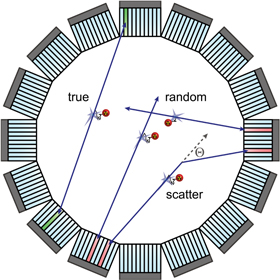
Figure 1. Schematic representation of a PET ring consisting of 16 detector modules. Also indicated are three types of coincident event: true, random, and scattered. See text for detailed explanation. Reproduced with permission from Seifert (2012).
Download figure:
Standard image High-resolution imagePET image quality is affected by various sources of error (Cherry 2006, Lewellen 2008, Peng and Levin 2010). For example, the system intrinsic spatial resolution is determined by the finite range of the positrons (typically <1 mm), the accolinearity of the annihilation quanta (<0.5°), the finite crystal pitch (typically <5 mm), and parallax effects in case the depth of interaction (DOI) in the crystal is unknown and the annihilation occurs off-center (such as the true event in figure 1). The image signal-to-noise ratio (SNR) is determined for a large part by counting statistics and, consequently, is limited by the radiotracer dose, the scan time, and the system sensitivity. The first two factors should be kept as small as possible, so it is imperative to maximize sensitivity.
In addition to counting statistics, the image SNR is affected by so-called 'randoms,' i.e. coincidences that do not originate from the same annihilation event, and 'scatters,' i.e. events in which at least one of the annihilation photons has scattered within the patient before being detected (figure 1). Clinical PET images are commonly corrected for randoms and scatters, but the statistical fluctuations in these contributions nevertheless worsen the image SNR. In fact, also the reconstructed spatial resolution of clinical PET images is often limited by the SNR rather than the system intrinsic spatial resolution. Thus, the importance of high sensitivity is hard to overestimate.
Details on the history, principles of operation, and technological development of PET can be found in several reviews, e.g. (Budinger 1998, Humm et al 2003, Cherry 2006, Muehllehner and Karp 2006). This particular selection of papers was written before time-of-flight (TOF) PET became widely used in clinical practice. Nevertheless, TOF-PET was already recognized as a promising innovation at the time.
1.1. TOF-PET
Figure 2 shows the principle of TOF-PET. The position of annihilation along the LOR is estimated based on the difference between the times of interaction of the annihilation quanta within the detector ring. The position uncertainty equals  where c is the speed of light in vacuum and
  the coincidence resolving time (CRT). The CRT characterizes the capability of a pair of detectors to resolve the difference in the times of interaction of two gamma quanta detected in coincidence. It is commonly quantified as the full-width-at-half-maximum (FWHM) of the spectrum of time differences measured for a large number of coincidences. Currently available TOF-PET scanners have coincidence resolving times of several hundred ps FWHM (averaged over the entire system). This is still insufficient to assign the annihilation event directly to a single image voxel. Nevertheless, the available TOF information can be used to limit the number of voxels to which activity is attributed during image reconstruction. This improves the quality of the resulting image in various ways, as discussed further in the following.

Figure 2. Principle of time-of-flight PET imaging; see text for explanation. Reproduced with permission from Philips and Andreas Thon.
Download figure:
Standard image High-resolution imageTOF-PET has rapidly become the clinical standard after a number of manufacturers released their first TOF-PET systems during the second half of the 2000s (Surti et al 2007, Bettinardi et al 2011, Jakoby et al 2011). CRT values have improved considerably, from about 500 - 700 ps FWHM for those scanners, to about 200–300 ps FWHM for the fastest machines available at the time of writing (Rausch et al 2019, van Sluis et al 2019). The beneficial effect of TOF-reconstruction on PET image quality is well established (Karp et al 2008, Conti 2009, 2011, Surti 2015, Surti and Karp 2016, Vandenberghe et al 2016, Berg and Cherry 2018a, Schaart et al 2020a). While it is not straightforward to quantify this benefit using a single number, it is generally agreed that the SNR improvement is proportional to:

with  the diameter of the imaged subject.
Thus, TOF is said to increase the effective sensitivity (the amount of information acquired per Bq s) of a PET scanner by a factor proportional to  which not only improves the SNR but also translates into better reconstructed resolution, contrast recovery, lesion detectability, and quantitative accuracy. TOF furthermore reduces patient-size dependence and makes it possible to reduce the administered radiotracer dose or scan time. Moreover, iterative image reconstruction converges faster and becomes more robust against inconsistent, incomplete, and/or incorrect data. As a consequence, TOF facilitates new approaches in image reconstruction, such as the joint estimation of emission and attenuation (Berker and Li 2016), utilizing the spatial information still carried by scatters (Conti et al
2012, Hemmati et al
2017), or reducing limited-angle artefacts in partial-ring and non-cylindrical systems, e.g. for particle therapy treatment verification or organ-specific imaging (Crespo et al
2007, Surti and Karp 2008, Parodi 2012, Lopes et al
2016, Gonzalez et al
2018, Yoshida et al
2020). Finally, the excellent imaging performance of current TOF-PET systems is opening up new clinical possibilities, in particular low-count applications such as immunoPET, theragnostics, imaging of 90Y radionuclide therapy, pediatric imaging, and screening of patients at risk (Conti and Bendriem 2019).
which not only improves the SNR but also translates into better reconstructed resolution, contrast recovery, lesion detectability, and quantitative accuracy. TOF furthermore reduces patient-size dependence and makes it possible to reduce the administered radiotracer dose or scan time. Moreover, iterative image reconstruction converges faster and becomes more robust against inconsistent, incomplete, and/or incorrect data. As a consequence, TOF facilitates new approaches in image reconstruction, such as the joint estimation of emission and attenuation (Berker and Li 2016), utilizing the spatial information still carried by scatters (Conti et al
2012, Hemmati et al
2017), or reducing limited-angle artefacts in partial-ring and non-cylindrical systems, e.g. for particle therapy treatment verification or organ-specific imaging (Crespo et al
2007, Surti and Karp 2008, Parodi 2012, Lopes et al
2016, Gonzalez et al
2018, Yoshida et al
2020). Finally, the excellent imaging performance of current TOF-PET systems is opening up new clinical possibilities, in particular low-count applications such as immunoPET, theragnostics, imaging of 90Y radionuclide therapy, pediatric imaging, and screening of patients at risk (Conti and Bendriem 2019).
1.2. TOF-PET detectors
The detector performance is the primary factor determining the image quality of a TOF-PET scanner. However, detector developers are faced with a large number of requirements that must be met. The spatial resolving power of the detector is important as it determines the system resolution. The detector must be able to measure the energy of the absorbed annihilation quanta to distinguish trues from scatters. High detection efficiency is paramount to assure sufficient image contrast. This also implies that the dead space between crystals must be kept as small as possible. Excellent detector time resolution is required as it determines the CRT at system level. In case the detectors are integrated with MRI equipment, the detector should be insensitive to magnetic fields and contain no magnetic components. The cost of fabrication, operation, and maintenance should be kept within certain limits and the detector performance should be stable in time. Other practical requirements include mechanical robustness, scalability, and low power consumption. Some of these requirements may be in conflict which each other and trade-offs may need to be made. For example, a design that offers excellent spatial resolution may not necessarily provide good time resolution.
The particular importance of PET system sensitivity has already been emphasized. In clinical practice, both the resolution and the contrast of PET images are often limited by a lack of counts, so an improvement of the detector spatial resolution is meaningful only if the (effective) sensitivity is improved as well (Phelps et al 1982). TOF improves the effective sensitivity in accordance with equation (1), but this gain applies only to the coincidences actually detected. To make rational trade-offs in TOF-PET detector design, one might define a simple figure of merit (FOM):

where  is the detection efficiency of the detectors for 511 keV photons,
  represents the system geometrical efficiency (solid angle subtended by the PET rings), and $ the total cost of the detectors. Thus,
  can be seen as a first-order estimate of the effective system sensitivity per unit cost. Note that
  is found squared in this equation because of the requirement to detect both of a pair of annihilation photons to form a LOR.
Equation (2) ignores the influence of spatial resolution, energy resolution, dead time, inter-crystal scatter, etc, on the quality of the reconstructed image. More detailed models, for example based on Monte Carlo simulation, may thus be necessary to make better informed trade-offs in the design of TOF-PET scanners (Jan et al
2004). Nevertheless,  is a useful FOM within the scope of this review, as it offers a simple means to put the improvement of timing performance into perspective (Schaart et al
2020a). For example, one may weigh the use of more expensive detector components against the possibility to increase
is a useful FOM within the scope of this review, as it offers a simple means to put the improvement of timing performance into perspective (Schaart et al
2020a). For example, one may weigh the use of more expensive detector components against the possibility to increase  by adding more detectors. As a second example, the term
  makes that little gain is to be expected when detection efficiency is traded for timing performance. As we well see later, this is a pitfall easily encountered in TOF-PET detector research.
This review aims to offer insight into the challenges encountered, solutions developed, and lessons learned in the development of TOF-PET detectors, with emphasis on the advances made in the last ∼15 years. The theory of scintillation detector timing is discussed first (chapter 2). The concepts and parameters defined in this chapter form the foundation for the remainder of the paper. Next, the recent developments with respect to the two principal components of a TOF-PET detector are reviewed: the scintillator (chapter 3) and the photosensor (chapter 4). Finally, the interplay between these components and the optimization of the overall detector design are discussed in chapter 5. Aspects of importance to the (electronic) optimization and processing of timing signals are addressed throughout this work.
The scope of this review primarily includes detectors based on fast, bright, inorganic scintillators, since these are used in essentially all TOF-PET systems in clinical use at the time of writing. While the focus is on the improvement of timing performance, an attempt is made to cover this subject from a clinically-driven perspective. That is, many hardware and software aspects determine the value of PET as a tool for research and (personalized) medicine and the CRT is just one parameter that can help to improve it. The best TOF-PET system is a well-balanced system, in which all factors of importance, including those summarized at the beginning of this section, are properly taken into account.
A large amount of literature is available on the topics discussed in this work, therefore full coverage is not attempted. Rather, representative examples are selected that illustrate the main achievements to date. Apologies are offered in advance to the authors of any relevant works that may have been overlooked in the process.
2. Fundamentals of scintillation detector time resolution
In principle, all of the components of the signal acquisition and processing chain affect the TOF performance of a PET system, including the scintillation detectors, readout electronics, digitization circuits, and signal processing methods. Nevertheless, the CRT of state-of-the-art TOF-PET scanners is primarily limited by the timing performance of the detectors, which contain scintillation crystals and photosensors as their main components. Consequently, this chapter focuses on the fundamentals of scintillation detector time resolution. A number of elementary concepts are introduced that will be used throughout the remainder of the paper. It is assumed that the scintillator is coupled to a light sensor with single-photon detection capability, as is the case in clinical TOF-PET scanners.
In any PET detector in which the energy of the annihilation quantum is converted into a luminescent signal, the stochastic nature of the physical processes governing the emission, transfer, and detection of the optical photons make that the optimization of time resolution is, in essence, a statistical problem. As illustrated in figure 3, the interaction of an annihilation photon at time  and position
  results in the emission of a discrete number
  of optical photons, at random times
  and in random directions
  from the point
  where
where  are unit vectors. In the case of a scintillator, for example,
  is non-Poisson-distributed around a mean value
  the emission is isotropic, and the times
  may be considered statistically independent and identically distributed (IID) in time according to a probability density function (PDF)
  which we will call the emission function. For many scintillators, the emission function can be described as a convolution of two exponential functions representing the energy transfer to the luminescence centers and their radiative decay, respectively:

with  and
and  the scintillation rise- and decay-time constants, respectively.
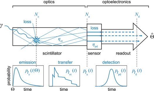
Figure 3. Schematic representation of the processes contributing to the uncertainty in the estimated time of interaction  See text for explanation.
Download figure:
Standard image High-resolution imageThe velocities of the optical photons may be considered equal and constant, at least in first-order approximation. That is,  with
with  the speed of light in vacuum and
  the refractive index of the luminescent material at the emission wavelength
  On the other hand, the path lengths
  between
  and the points at which the photons are absorbed by the light sensor may vary significantly (figure 3). Moreover, photons may escape and/or be absorbed (and, potentially, re-emitted) within the luminescent material, reflectors, coupling compounds, light guides, and/or dead regions of the light sensor. These optical processes give rise to statistical fluctuation of (1) the number of photons
  arriving at the photosensitive region per event and (2) the distribution of the times
  at which these photons arrive. The expectation value of
  equals
  with
with  the optical transfer efficiency (OTE). The distribution in time of
  may be described using a PDF
  which we will call the photosensor illumination function. This function equals the convolution of
  and what we will call the optical transfer time distribution,
  which governs the optical transfer times
  of the individual photons to the photosensor:

The FWHM of  will be called the optical transfer time spread (OTTS) and can be seen as a measure of the loss of time information due to the kinetics of optical transfer.
Additional deterioration of time information occurs within the light sensor and the associated readout electronics. First, only a fraction  of the photons arriving at the photosensitive region is detected (i.e. gives rise to an electrical signal). The parameter
  is called the photodetection efficiency (PDE). Second, if the light sensor is illuminated with single photons, the delay between the
  and the times
  at which the photons are electronically detected shows some variation from photon to photon. The single-photon timing spectrum (SPTS), which will be written as
  describes the distribution of these photon detection delays
  The FWHM of
  is called the single-photon time resolution (SPTR) or, in the specific case of a vacuum photomultiplier tube (PMT), the transit time spread (TTS).
Finally, the CRT is affected by the efficiency of the method used to estimate the time of interaction  The available time information is carried by the
  photons actually detected,
  having an expected value
  In principle, the maximum amount of time information is available if the signal acquisition and processing chain is capable of assigning a timestamp to each detected photon, resulting in a set of timestamps
  randomly distributed in time according to the detected photon distribution:

In practice, it is difficult to measure the full set  For example, the single-photoelectron response (SER) of a PMT (i.e. the output pulse in response to a single detected photon) may be substantially longer than the difference between the arrival times of consecutive scintillation photons. In that case, multiple single-photoelectron pulses contribute to the signal amplitude at any time
  making it difficult to timestamp individual photons. As a matter of fact,
  is often estimated using much simpler methods, e.g. by feeding the detector output signal into a leading-edge discriminator (LED) or a constant-fraction discriminator (CFD) (Knoll 2010). Interestingly, we will find that such straightforward estimators can be quite efficient, since most of the time information is contained in the early part of the light signal (section 2.4).
2.1. Modeling time resolution: Monte Carlo approaches
Given the stochastic nature of the generation, transfer, and detection of the optical information carriers, Monte Carlo simulation appears as an obvious approach for modeling the time resolution of scintillation detectors. Indeed, time-resolved Monte Carlo simulations were applied to PMT/scintillator systems in the 1960s already (Hyman et al 1964, Gatti and Svelto 1966). They were also used to better understand the physical effects that limited the time resolution of the first TOF-PET research systems in the late 1980s (Tzanakos et al 1990, Ziegler et al 1990).
A variety of TOF-PET scintillation detectors have been simulated in the last decade. These works illustrate how Monte Carlo simulations can be used to obtain quantitative information about the influence on the CRT of, for example, the generation and transfer of the optical quanta (Yang et al 2013, Derenzo et al 2014, Gundacker et al 2014, Roncali et al 2014, Berg et al 2015, Ter Weele et al 2015c), the choice of photosensor and optical readout geometry (Liu et al 2009, Derenzo et al 2015, Gundacker et al 2015), the characteristics of the readout electronics (Powolny et al 2011, Brekke et al 2012), and the method used for time pick-off (Choong 2009, Brunner et al 2013, Venialgo et al 2015).
In general, it appears less than trivial to reproduce experimental timing results in silico. Accurate modeling of the photon transport kinetics, for example, requires detailed information on the optical material properties (Roncali et al 2017). Similarly, the (opto-)electronic characteristics of the light sensor and the readout electronics are often simplified, which can easily lead to overly optimistic predictions regarding the CRT. Nevertheless, carefully performed Monte Carlo simulations can help to make informed decisions and trade-offs in detector design.
2.2. Modeling time resolution: analytical approaches
The Monte Carlo method offers versatility, but is computationally expensive and provides results for a single combination of input settings only. An analytical model, on the other hand, provides a mathematical formulation of the performance over a wide range of working conditions.
Post and Schiff (1950) considered the limitations on the resolving time of a PMT-based scintillation detector that arise from the fluctuations in the emission and detection of the scintillation photons, if the PMT output signal is fed into a time-pickoff circuit that generates a timestamp when a given number of single-photoelectron pulses has been accumulated. In terms of the parameters introduced at the beginning of this chapter, they calculated the uncertainty in  as a function of
  Approximations used in the model are that
  is a single-exponential decay function (i.e.
  ), the transfer of scintillation photons to the photocathode is instantaneous (i.e.
  see equation (4)), the number of photoelectrons
  follows a Poisson distribution, and the photomultiplier TTS equals zero (i.e.
  see equation (5)). Post and Schiff thus arrived at an asymptotic series expression for the variance of

This result suggests that the time pickoff circuit should trigger on the first detected photon ( ) to obtain the best possible timing. In modern TOF-PET detectors, however, the best CRT is generally achieved at
  This is because equation (6) is valid only if the underlying assumptions are met, in particular if the scintillator rise time, the OTTS, and the photomultiplier TTS all are negligibly small compared to the expected time difference between
  and
and  for all
  This is not the case for the fast and bright scintillators used in current PET systems, for which
  is in the order of a few picoseconds around
  Thus, a more refined timing model is needed to accurately predict the CRT of modern TOF-PET detectors.
Hyman et al (1964) and Hyman (1965) developed a model of scintillation detector time resolution in which  is taken into account, i.e. they modeled
  according to equation (3). They furthermore included the photomultiplier SER, the TTS, and the gain dispersion
  which arises from statistical fluctuations in the multiplication process. Hyman et al assumed that
  is Poisson-distributed and the SER and TTS can be modeled as truncated Gaussian functions, while they considered optical transfer to be instantaneous (i.e.
  see equation (4)). They considered different modes of electronic processing for deriving a timestamp from a PMT anode pulse and presented their results using plots of what is nowadays called the Hyman function
  where
where  and
and  are the standard deviations used to model the SER and the TTS, respectively, while
  is the trigger threshold as a fraction of the total pulse height. The standard uncertainty in the estimate of
  can then be described as:

For 
 becomes proportional to
  In other words,
  if the scintillator has negligible rise time, as has been confirmed experimentally by e.g. (Szczȩśniak et al
2009).
if the scintillator has negligible rise time, as has been confirmed experimentally by e.g. (Szczȩśniak et al
2009).
Gatti and coworkers also developed a theory of time resolution in scintillation counters, analyzing the statistical properties of the PMT in great detail (Gatti and Svelto 1964, 1966, Donati 1969, Donati et al
1970). Furthermore, Donati et al (1970) investigated the influence of an approximation made in their own theory as well as in those of others, namely that the uncertainty in  can be estimated as the uncertainty in the amplitude, divided by the expected slope, of the photosensor output pulse at
  This is valid in the absence of pulse shape variation and if the slope is constant over a time period larger than the uncertainty in
  These conditions are asymptotically satisfied when the expected number of photoelectrons
  is large. However, Donati et al (1970) showed that the approximate calculation can be overly optimistic compared to the exact calculation at small values of
  which may e.g. be of importance when modeling the time resolution achievable with weak (e.g. Cherenkov) emissions.
All of the above models ignore the transfer of scintillation light to the photocathode. In other words, they predict the time resolution in what could be called the 'infinitesimal-crystal approximation.' Cocchi and Rota (1967) analyzed how the OTTS affects the time resolution for cylindrical scintillators of finite dimensions. They showed that  cannot be neglected for crystal dimensions in the order of cm when interpreting the results of timing experiments in the range of a few hundred picoseconds. Bengtson and Moszynski (1970) added this contribution to the Hyman model by folding
  with
with  as in equation (4), simplifying
  to a single-exponential decay function (
 ) and describing
  as a Gaussian. They reported quantitative agreement between the resulting model and experiments performed with fast plastic scintillators. They furthermore compared leading-edge triggering with constant-fraction discrimination, reporting that a CFD provided better timing even if only events within a relatively narrow range (20%) of pulse heights were selected.
It may be evident that the timing properties of PMT-based scintillation detectors have been well understood since the 1970s. Section 4.2 gives examples of how this knowledge can be utilized to improve PMTs for timing purposes.
Unfortunately, PMT timing theory cannot be extrapolated straightforwardly to detectors based on solid-state photosensors, such as silicon photomultipliers (SiPMs), as these sensors have fundamentally different characteristics. Therefore, Seifert et al (2012c) developed and experimentally validated a more general, fully probabilistic model of the time resolution of scintillation detectors, which can account for SiPM-specific properties such as a highly asymmetric shape of the output pulse in response to single photons and the occurrence of crosstalk, as well as electronic noise. Moreover, they used a more detailed model of the scintillator, which allows multiple cascades of processes to contribute to the emission and takes into account the true (i.e. non-Poissonian) variance of 
The Seifert model is discussed in more detail in section 4.3.4. That section also describes the practical implications of the model for optimizing the timing properties of SiPM-based scintillation detectors. It is noted that this model reduces to the Hyman model in the special case that  is Poisson-distributed and crosstalk and electronic noise are negligible; in other words, when the photosensor properties are assumed to correspond to those of a PMT according to Hyman.
2.3. Modeling time resolution: Cramér–Rao analysis
Section 2.2 covered analytical models of increasing complexity, describing the different contributions to the time resolution of scintillation detectors in more and more detail. State-of-the-art TOF-PET systems utilize bright scintillators in combination with photodetectors with high internal gain and optimized readout electronics. In such systems, the influence of noise and other electronic factors on the CRT is minimized and, as a consequence, the CRT is primarily limited by photon counting statistics, as determined by the emission, transfer, and detection of the scintillation photons. Moreover, all of the models discussed in section 2.2 were derived on the basis of certain assumptions with respect to the estimator used to derive a timestamp from the detector signal. This raises the question if a CRT better than that predicted by the model could be achieved with a different type of estimator.
In view of the above arguments, it appears useful to derive a model that focuses on photon-counting statistics and that quantifies the potential timing performance of a scintillation detector, independently of the estimator used. Such a model can be utilized, for example, to rationally optimize a hardware design and/or to calculate an objective reference against which the performance of a timing algorithm can be compared. It furthermore makes sense to structure such a model in accordance with the overall architecture of the data acquisition and readout chain, which comprises an optical part and an optoelectronic part (figure 3). In terms of the parameters introduced at the beginning of this chapter, the output of the optical part can be characterized by the probability distribution of the number of photons  arriving at the photosensor and the illumination function
  defined in equation (4). The optoelectronic part, comprising the photosensor and the associated readout electronics, can be characterized by the PDE
  and the SPTS
  We thus describe the timing branch of the data acquisition and readout chain as a series of stochastic processes undergone by the individual carriers of time information. This approach should allow us to build a statistical model of time resolution. Ideally, the formalism would accept any function or empirically derived histogram for each of the pertinent PDFs.
Seifert et al (2012b) used the Cramér–Rao lower bound (CRLB) to arrive at such a model. In its simplest form, the CRLB equals the minimum value of the variance that any unbiased estimator  of a given parameter
  can achieve on the basis of
  independent measurements of a random variable
  that is distributed according to some PDF

where the so-called Fisher information  is given by:

An estimator that achieves the CRLB is said to be (fully) efficient. For example, it can be shown that the maximum likelihood (ML) estimator is asymptotically efficient, if an efficient estimator exists. That is, if  independent measurements are made for the same value of the unknown parameter, the ML estimator achieves the CRLB for
  (Barrett and Myers 2004, 893 ff).
Under the assumption that the time information carried by all detected photons, i.e. the entire set of timestamps  introduced at the beginning of this chapter, can be used to derive an estimator
  of the time of interaction
  the Cramér–Rao inequality takes the relatively simple form:

where  is the probability density of photon detection, given
  as defined in equation (5).
It is possible to express  in analytical form if the scintillation pulse is described according to equation (3). To this end, it is practical to fold
  and
and  into a single PDF governing the time
  taken up by the complete transfer of an information carrier from emission to detection (shifting shape from a photon to an electronic signal along the way):

If this function is approximated by a Gaussian with mean  and standard deviation
  it can be shown that equation (5) can be written as follows:

where:

In addition to equation (10), Seifert derived expressions for the CRLB in cases where  is based on subsets of the ordered set
  which is obtained by sorting the non-ordered set
  in ascending order. Specifically, he derived the CRLB for the case that only the nth rank,
  is known, and for the case that the
  smallest timestamps,
  are available for estimating
  The relevance of calculating the CRLB for such subsets of
  lies in the observation that a relatively small number of early-detected photons carry most of the time information in a typical TOF-PET detector (see section 2.4). The derivation of the CRLB for subsets of
  involves order statistics, since
  and
and  change the photon order between emission and detection. Fishburn and Charbon (2010) also explored the use of order statistics, in the context of optimizing single-photon avalanche diode/time-to-digital converter (SPAD/TDC) arrays for the readout of scintillators. Mandai et al (2014) provided direct experimental evidence for the validity of applying order statistics to photon counting problems. They illuminated a so-called multichannel digital silicon photomultiplier (MD-SiPM) with faint, 374 ps FWHM Gaussian laser pulses, measured the probability distribution of
  for
for  and found them to be in agreement with the corresponding theoretical PDFs.
Various authors have proposed extensions of Seifert's theory. For example, Cates et al (2015) derived an analytical expression for  applicable to the case of polished, high-aspect-ratio scintillation crystals. They used this expression to obtain a mathematical expression of the CRLB for this case, assuming
  to be Gaussian. Venialgo et al (2015) examined the CRLB for the MD-SiPM. This device comprises
  SPADs and
  TDCs, where
  If
If  it timestamps the
  first-detected photons. If this condition is not met, however, a more random subset of
  is selected.
Toussaint et al (2019) recently proposed and experimentally validated (Loignon-Houle et al
2020) an important extension of Seifert's model that takes into account the influence of DOI variation on the CRLB in long crystals. The position of interaction  is one of the parameters determining the optical transfer kinetics, an effect not taken into account in the original formulation of the Seifert model. In fact,
  influences both the mean and the variance of
  That is, the expected arrival time of the scintillation photons at the photosensor, given
  varies with
  due to the difference between the velocities of the annihilation photon and the light signal within the crystal (Moses and Derenzo 1999). This introduces an
  -dependent bias in the estimated time of interaction
  In addition, the distribution of possible optical path lengths and, therefore, the variance of
  may change with
  Thus, it is in fact more accurate to write the optical transfer time distribution as
  This, in turn, implies that we should rewrite the detected photon distribution originally defined in equation (5) as follows:

where  is the convolution operator.
Toussaint et al (2019) discuss three important consequences of this redefinition of  A first consequence is that the Fisher information (equation (9)) is defined for a given position of interaction
  only:
only:

Therefore, the same is true for the CRLB on the estimated time of interaction in the detector:

As a second consequence, the variation of the mean of  and, therefore,
  with
with  introduces a position-of-interaction-dependent bias in the estimated time of interaction in case
  is unknown:

Third, the positions of interaction  and
and  in two coincident detectors A and B vary independently. Thus, the variances
 ![${\rm{Var}}\,[{\hat{{\rm{\Theta }}}}_{{\vec{x}}_{{\rm{A}}}}]$](https://content.cld.iop.org/journals/0031-9155/66/9/09TR01/revision3/pmbabee56ieqn204.gif) and
and ![${\rm{Var}}\,[{\hat{{\rm{\Theta }}}}_{{\vec{x}}_{{\rm{B}}}}]$](https://content.cld.iop.org/journals/0031-9155/66/9/09TR01/revision3/pmbabee56ieqn205.gif) as well as the biases
as well as the biases ![${\rm{Bias}}\,[{\hat{{\rm{\Theta }}}}_{{\vec{x}}_{{\rm{A}}}}]$](https://content.cld.iop.org/journals/0031-9155/66/9/09TR01/revision3/pmbabee56ieqn206.gif) and
and ![${\rm{Bias}}\,[{\hat{{\rm{\Theta }}}}_{{\vec{x}}_{{\rm{B}}}}]$](https://content.cld.iop.org/journals/0031-9155/66/9/09TR01/revision3/pmbabee56ieqn207.gif) in the two detectors vary independently from event to event. The same is necessarily true for the variance and the bias of the estimated parameter of interest, i.e. the estimated time difference
in the two detectors vary independently from event to event. The same is necessarily true for the variance and the bias of the estimated parameter of interest, i.e. the estimated time difference 
The mean squared error is commonly used to characterize the performance of a biased estimator. To account for the above three consequences of the position-of-interaction dependence of  Toussaint et al (2019) propose the lower bound on the root mean square error (RMSE) over all possible combinations of
  and
and  as a measure of the best achievable CRT:

Here, ![${\rm{Var}}\,[{\hat{{\rm{\Theta }}}}_{{\rm{AB}}}]={\rm{Var}}\,[{\hat{{\rm{\Theta }}}}_{{\vec{x}}_{{\rm{A}}}}]+\,{\rm{Var}}\,[{\hat{{\rm{\Theta }}}}_{{\vec{x}}_{{\rm{B}}}}]$](https://content.cld.iop.org/journals/0031-9155/66/9/09TR01/revision3/pmbabee56ieqn212.gif) is the sum of the lower bounds on the variances of the two detectors, given
is the sum of the lower bounds on the variances of the two detectors, given  and
and  calculated according to equation (16). Furthermore,
 ![${\rm{Bias}}\,[{\hat{{\rm{\Theta }}}}_{{\rm{AB}}}]={\rm{Bias}}\,[{\hat{{\rm{\Theta }}}}_{{\vec{x}}_{{\rm{A}}}}]-{\rm{Bias}}\,[{\hat{{\rm{\Theta }}}}_{{\vec{x}}_{{\rm{B}}}}]$](https://content.cld.iop.org/journals/0031-9155/66/9/09TR01/revision3/pmbabee56ieqn215.gif) is the total bias on the estimated time difference, given
is the total bias on the estimated time difference, given  and
and  Finally, the PDFs
  and
and  describe the probability distributions of
  and
and  respectively, given that a coincidence is registered by the detector pair AB.
Toussaint et al (2019) note that the practical application of equation (18) may be less straightforward since the bias function ![${\rm{Bias}}\,[{\hat{{\rm{\Theta }}}}_{{\rm{AB}}}]$](https://content.cld.iop.org/journals/0031-9155/66/9/09TR01/revision3/pmbabee56ieqn222.gif) of the best estimator may be unknown. They investigate a surrogate function based on the shortest path from the point of emission to the photosensor, which appears to work for extremely bright scintillators only. Alternatively, surrogate functions could be obtained from Monte Carlo simulations or, since the absolute biases defined in equation (17) are not needed to calculate their difference, from experiments similar to those of Moses and Derenzo (1999) and Van Dam et al (2013). A function thus obtained remains a surrogate of
of the best estimator may be unknown. They investigate a surrogate function based on the shortest path from the point of emission to the photosensor, which appears to work for extremely bright scintillators only. Alternatively, surrogate functions could be obtained from Monte Carlo simulations or, since the absolute biases defined in equation (17) are not needed to calculate their difference, from experiments similar to those of Moses and Derenzo (1999) and Van Dam et al (2013). A function thus obtained remains a surrogate of ![${\rm{Bias}}\,[{\hat{{\rm{\Theta }}}}_{{\rm{AB}}}]$](https://content.cld.iop.org/journals/0031-9155/66/9/09TR01/revision3/pmbabee56ieqn223.gif) in the sense that one needs to make assumptions with respect to the best possible time estimator to determine it.
in the sense that one needs to make assumptions with respect to the best possible time estimator to determine it.
Equation (18) applies if  and
and  are unknown. In case the positions of interaction are known and used to (perfectly) correct
  for the corresponding bias, the term
 ![${({\rm{Bias}}\,[{\hat{{\rm{\Theta }}}}_{{\rm{AB}}}]\,)}^{2}$](https://content.cld.iop.org/journals/0031-9155/66/9/09TR01/revision3/pmbabee56ieqn227.gif) disappears from the equation. It is furthermore noted that
disappears from the equation. It is furthermore noted that  and
and  can sometimes be reduced to just the depths of interaction
  and
and  respectively, for example in high-aspect-ratio crystals. However, the present formulation makes equation (18) applicable to other detector geometries, such as monolithic scintillators (section 5.4). As a final note,
 ![${\rm{Var}}\,[{\hat{{\rm{\Theta }}}}_{{\rm{AB}}}]$](https://content.cld.iop.org/journals/0031-9155/66/9/09TR01/revision3/pmbabee56ieqn232.gif) and
and ![${\rm{Bias}}\,[{\hat{{\rm{\Theta }}}}_{{\rm{AB}}}]$](https://content.cld.iop.org/journals/0031-9155/66/9/09TR01/revision3/pmbabee56ieqn233.gif) are often determined for discrete values of
are often determined for discrete values of  and
and  in practice, in which case equation (18) needs to be approximated by a Riemann sum.
The CRLB approach is quite generally applicable. For example, Seifert et al (2012b) acknowledged that multiple cascades of energy transfer and luminescent processes may occur in a given scintillator and consequently allowed  to be written as a linear combination of emission profiles according to equation (3). Furthermore, there is no necessity to express the detected photon distribution in analytical form, as in equation (12). In fact, equation (10) can be evaluated for any
  that fulfills two weak regularity conditions associated with the CRLB, viz, that the Fisher information is always defined and that differentiation with respect to
  and integration with respect to
  are interchangeable (Arnold et al
2008). For the latter condition to be fulfilled, it is generally sufficient that the bounds of
are interchangeable (Arnold et al
2008). For the latter condition to be fulfilled, it is generally sufficient that the bounds of  in
in  are independent of
  It is noted that this is not the case if
  is simplified to the emission function defined in equation (3). The condition is fulfilled, however, if
  is defined according to equation (5) and
  and/or
  have infinite support. Such is the case, for example, if we model any of these functions, or, equivalently,
  defined in equation (11), by a Gaussian. In fact, we may even truncate
  at
at  to avoid negative timestamps, provided that
  This was done in the original paper by Seifert et al (2012b), for example. The practical consequences of these observations are that there is no need to describe
  or
or  analytically and that they can be obtained independently, whether from measurement, Monte Carlo simulation, or analytical modeling, as long as we make sure that no significant breaching of the regularity conditions occurs.
The representation of the CRLB in terms of the parameters introduced at the beginning of this chapter allows groups working on different components of the TOF-PET detection chain, such as scintillators, photosensors, electronics, and data processing algorithms, to optimize their results independently and objectively. Indeed, the model and its extensions are used for such purposes by various authors, e.g. (Ter Weele et al 2015a, Cates and Levin 2018). Moreover, the model is useful for explaining and quantifying general trends and dependencies in scintillation detector timing performance. This will be elaborated in section 2.4. However, let us first examine some limitations and pitfalls of the CRLB.
An essential assumption in the Seifert model is that the  are IID. Fortunately, this requirement is generally met in TOF-PET detectors, especially for the early-detected photons that carry most of the time information. Furthermore, the total number of detected photons
  in equation (10) is fixed. Similar to the position of interaction in equation (18), its variation from event to event can be taken into account by calculating the weighted average of the CRLB over the possible values of Nd. In this way, Seifert et al (2012b) showed that the spread in
  contributes negligibly to the CRT for bright TOF-PET scintillators with an energy resolution in the order of ∼10% FWHM. It is emphasized, however, that equation (10) may no longer be valid if the energy resolution gets worse, e.g. because
  itself becomes small. Straightforward application of the CRLB model to Cherenkov photons, as done by Gundacker et al (2016, 2018) and Lecoq (2017), Lecoq et al (2020), for example, could therefore yield overly optimistic results.
Another, more fundamental limitation of the CRLB is that it may approach the trivial case ![${\rm{Var}}\,[\hat{{\rm{\Theta }}}]\geqslant 0$](https://content.cld.iop.org/journals/0031-9155/66/9/09TR01/revision3/pmbabee56ieqn257.gif) for nearly-nondifferentiable
for nearly-nondifferentiable  Also this limitation is relevant to weak emissions, in particular those with one or more sharp edges in their emission function. More specifically, if
  and
and  over a finite interval of time, the integral in equation (10) may become very large and, as a result, the term on the right-hand side of the equation may tend to zero. For these reasons, Hero (1989) and Clinthorne et al (1990b) have studied alternative bounds that may be more tight than the CLRB, for example for nearly-exponentially decaying scintillators with a low light yield, such as BGO. However, they found these alternative bounds to be superseded by the CRLB for bright scintillators (Clinthorne et al
1990a). Thus, it may be concluded that the CRLB is a useful measure of the CRT achievable with the scintillators commonly used in TOF-PET systems today. Indeed, experimental results very close to the CRLB have been achieved with various types of crystal and photosensor (Schaart et al
2010, Schmall et al
2014, Cates and Levin 2016, Gundacker et al
2019).
over a finite interval of time, the integral in equation (10) may become very large and, as a result, the term on the right-hand side of the equation may tend to zero. For these reasons, Hero (1989) and Clinthorne et al (1990b) have studied alternative bounds that may be more tight than the CLRB, for example for nearly-exponentially decaying scintillators with a low light yield, such as BGO. However, they found these alternative bounds to be superseded by the CRLB for bright scintillators (Clinthorne et al
1990a). Thus, it may be concluded that the CRLB is a useful measure of the CRT achievable with the scintillators commonly used in TOF-PET systems today. Indeed, experimental results very close to the CRLB have been achieved with various types of crystal and photosensor (Schaart et al
2010, Schmall et al
2014, Cates and Levin 2016, Gundacker et al
2019).
2.4. Summary and general observations from timing theory
A general framework for describing the factors that affect the time resolution of scintillation detectors was introduced at the beginning of this chapter. Figure 3 provides a schematic overview of the pertinent processes and the functions and parameters used to describe them. These can be classified according to whether they relate to the emission, transfer, or detection of scintillation photons. The stochastic nature of these processes warrant Monte Carlo modeling (section 2.1), even though it may take considerable effort to obtain all required input parameters with sufficient accuracy. Several authors have proposed analytical models of scintillation detector time resolution, which vary in the level of detail in which the three categories of processes are described (section 2.2). In section 2.3, it was argued that photon-counting statistics form the dominant contribution to the CRT of state-of-the-art TOF-PET detectors based on bright scintillators and photosensors with high internal gain. As a consequence, the CRLB on the time resolution provides a useful measure of the achievable time resolution. The CRLB can be used, for example, to better understand fundamental limitations, to benchmark detector performance, and to make rational design choices in the development of detectors, detector components, and timing algorithms.
A number of general conclusions can be drawn from the currently available theory. It is emphasized that these apply to detectors based on fast and bright scintillators (some observations relevant to other cases are discussed in section 5.5). The CRT is proportional to  in this case. This, in turn, implies that
 and
and  all are equally important for optimum time resolution. Furthermore, if
  is much larger than each of the scintillator rise time, the OTTS, and the SPTR, as is commonly the case, the CRT is also proportional to
  In first order approximation,
  therefore is a useful FOM for optimizing the intrinsic properties of a TOF-PET scintillator. The scintillator rise time only becomes important if it is larger than both the OTTS and the SPTR, in which case the CRT also becomes proportional to
It is noted that the maximization of  while important, is not sufficient to guarantee the best possible timing performance. For example, crystals that exhibit self-absorption of scintillation photons with a near-unit probability of re-emission may show a high integral light output, but the process of absorption and delayed re-emission increases the OTTS. This may lead to the seemingly paradoxical situation that a detector exhibits excellent energy resolution but a worse-than-expected CRT (van Dam et al
2012a, Ter Weele et al
2014a). Thus, an ideal TOF-PET detector design ensures not only efficient, but also rapid transfer of the scintillation photons to the photosensor.
while important, is not sufficient to guarantee the best possible timing performance. For example, crystals that exhibit self-absorption of scintillation photons with a near-unit probability of re-emission may show a high integral light output, but the process of absorption and delayed re-emission increases the OTTS. This may lead to the seemingly paradoxical situation that a detector exhibits excellent energy resolution but a worse-than-expected CRT (van Dam et al
2012a, Ter Weele et al
2014a). Thus, an ideal TOF-PET detector design ensures not only efficient, but also rapid transfer of the scintillation photons to the photosensor.
Indeed, the minimization of time resolution loss due to optical transfer kinetics is becoming an important research topic. All the more so, because the intrinsic rise time of the most commonly used TOF-PET scintillators (see table 1) and the SPTR of some photosensors are smaller than 100 ps already. The scintillator-photosensor geometry and the optical properties of the crystals, reflectors, light guides, and photosensors all affect  Intuitively, one would expect the use of larger crystals and/or complicated light-sharing schemes to broaden this distribution. Indeed, the best CRTs are often achieved with tiny crystals coupled one-to-one to photosensors, approaching the infinitesimal-crystal limit discussed previously. In fact, we have seen in section 2.3 that the optical transfer time distribution not only broadens in larger crystals, but that its mean and variance also become functions of the position of interaction
  resulting in additional deterioration of the CRT (equation (18)). TOF-PET detector designs that enable the estimation of
  often called TOF/DOI detectors allow to (partially) recover the resulting loss of time information, as will be elaborated in sections 5.3 and 5.4.
Table 1. Overview of TOF-PET scintillators and their properties. Data were taken from the publications cited in chapter 3. Uncertainties are in the order of one last digit, unless (a) the value is preceded by a tilde, e.g. '∼42', in which case the uncertainty is larger, or (b) a range of values is given, e.g. '40–44', in which case this range reflects the spread encountered in the papers cited. The value of  is placed within brackets, e.g. '(42)', if the magnitude of
  is such that this figure of merit may give an overly optimistic indication of the material's timing potential, i.e. if the condition
  is not necessarily fulfilled when the material is read out using a state-of-the-art photosensor. The energy resolution is given for 662 keV photon irradiation.

|

|

|

|

|

| Energy resolution | |||||
|---|---|---|---|---|---|---|---|---|---|---|---|
| Scintillator | Formula | Hygro-scopic | (g cm−3) |

|

| (nm) | (MeV−1) | (ps) | (ns) | (MeV−1/2 ns−1/2) | (% FWHM) |
| BaF2 | BaF2 | Slightly | 4.9 | 54 | 1.5 | 220 | 1300–1400 | — | 0.8 | ∼41 | 8 |
| CeBr3 | CeBr3 | Yes | 5.2 | 46 | — | 380 | 57 000–66 000 | < 200 | 17 | ∼60 | 4 |
| CsF | CsF | Yes | 4.6 | 52 | 1.5 | 390 | 1900–2000 | — | 3 | ∼25 | ∼20 |
| GAGG:Ce | Gd3Al2Ga3O12:Ce | No | 6.6 | 53 | 1.9 | 520 | 42 000–57 000 | 500–1800 | 50–120 (60%–95%) + 200–400 (5%–40%) | (∼21) | 5 |
| Gd3Al(5−x)Ga(x<3)O12:Ce | No | 6.5 | 53 | 1.9 | 520 | 50 000–58 000 | — | 140–200 (70%–95%) + slow (> 600) | (∼16) | 4 | |
| Gd3Al(5−x)Ga(2.4<x<3)O12:Ce,Mg | No | 6.6 | 53 | 1.9 | 520 | 43 000–47 000 | 50–70 | 40–50 (55%–65%) + 100–200 (35%–45%) | ∼24 | 6 | |
| Gd3Ga3Al2O12:Ce (ceramic) | No | 6.6 | 53 | — | ∼550 | 30 000–70 000 | — | 50–170 + slower | ∼20 | ∼5 | |
| GLuGAG:Ce | (Gd,Lu)3(Al,Ga)5O12:Ce (ceramic) | No | 6.7–6.9 | 53 | — | ∼550 | 20 000–50 000 | — | 40–90 + slower | ∼20 | ∼7 |
| LaBr3:Ce | LaBr3:Ce(5%) | Yes | 5.1 | 45 | 2.0–2.3 | 380 | 64 000–76 000 | 180–380 (60%–70%) + slow (> 1000) | 16 | (∼66) | 3 |
| LaBr3:Ce(>10%) | Yes | 5.1 | 45 | 2.0–2.3 | 380 | 68 000–70 000 | 100–200 (≥95%) | 16–18 | ∼64 | 3 | |
| LaBr3:Ce(5%),Sr | Yes | 5.1 | 45 | 2.0–2.3 | 380 | ∼78 000 | > 200 | 18 (80%) + slow | (∼60) | 2 | |
| LFS-3 | Cex Lu2+2y−x−z Az SiO5+y | No | 7.3 | 65 | 1.8 | 420 | ∼38 000 | < 100 | 35–40 | ∼32 | 8 |
| A = Ca, Gd, Sc, Y, La, Eu, Tb | |||||||||||
| LGSO-Fast | Lu2(1−x)Gdx SiO5:Ce(0.025%) | No | 7.2 | 66 | 1.8 | 420 | ∼34 000 | ∼10 | 30–34 | ∼32 | 8 |
| LSO:Ce | Lu2SiO5:Ce | No | 7.4 | 66 | 1.8 | 420 | 26 000–32 000 | < 100 | 39–43 | ∼27 | 8 |
| Lu2SiO5:Ce,Ca | No | 7.4 | 66 | 1.8 | 420 | 32 000–39 000 | < 100 | 31–37 | ∼32 | 8 | |
| LYSO:Ce | Lu2(1−x)Yx SiO5:Ce | No | 7.1 | 65 | 1.8 | 420 | 26 000–34 000 | < 100 | 38–44 | ∼27 | 8 |
| Lu2(1−x)Yx SiO5:Ce,Ca | No | 7.1 | 65 | 1.8 | 420 | 33 000–40 000 | < 100 | 33–39 | ∼32 | 8 | |
| LuI3:Ce | LuI3:Ce | Yes | 5.6 | 60 | — | ∼500 | ∼100 000 | — | ∼30 | ∼50 | ∼3 |
From the foregoing discussion, it may be clear that the PDE and the SPTR are the crucial parameters determining the time resolution that can be obtained with a given photosensor. Indeed, the improvement of these parameters is the objective of much photosensor research and an important driver of progress in TOF-PET performance, as will be elaborated in chapter 4.
All timing models that take into account the scintillator rise time, the OTTS, and/or the SPTR show that the timestamp with the lowest variance is not necessarily associated with the first photon detected. Moreover, the CRT may be smaller than the rise time, the OTTS, and/or the SPTR, provided that the scintillator is sufficiently bright. Both effects can be observed in figure 4 (left), where the black crosses show the CRLB based on a single timestamp  as a function of
  for small LYSO:Ce crystals coupled to SiPMs with an SPTR of 282 ps FWHM. The best CRT has less than half the value of the SPTR and is reached around
  These phenomena are direct consequences of the ordering of the set
  That is, a given rank
  can only be that rank if it is not another rank
  This condition makes that the probability distribution of each rank,
  becomes narrower when the average time between consecutive ranks becomes smaller, i.e. when the scintillator becomes brighter. Moreover, the width of
  is expected to be smallest around the time at which the photon detection rate is highest, i.e. at the maximum, rather than the onset, of
  as can be observed in figure 4 (right).
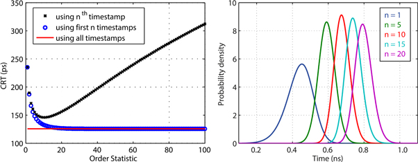
Figure 4. Left: Cramér–Rao lower bound on the CRT of 3 mm × 3 mm × 5 mm LYSO:Ce crystals coupled to Hamamatsu MPPC-S10362-33-50C SiPMs, for estimators based on a single timestamp  (black crosses) and estimators based on the first n timestamps
  (blue circles), as a function of n. The red solid line indicates the intrinsic limit on the time resolution that could be achieved if all timestamps were used (Adapted from Seifert: et al
2012b). © 2012 Institute of Physics and Engineering in Medicine. All rights reserved. Right: probability density functions
(blue circles), as a function of n. The red solid line indicates the intrinsic limit on the time resolution that could be achieved if all timestamps were used (Adapted from Seifert: et al
2012b). © 2012 Institute of Physics and Engineering in Medicine. All rights reserved. Right: probability density functions  of different ranks
  for the same detector.
Download figure:
Standard image High-resolution imageFinally, we may compare the blue circles in figure 4 (left), representing the CRLB based on the first  timestamps
  as a function of
  with the red solid line, which indicates the CLRB based on the entire set
  The CRT that can be achieved with the first
  timestamps approaches the intrinsic limit of the detector timing performance around
  (whereas
  ). Moreover, the CRLB for the optimum single-photon timestamp (
 ) is within ∼15% of the same limit (black crosses). These results are specific for the crystal-sensor combination considered, but illustrate the general finding that a relatively small number of early-detected photons carry most of the time information in state-of-the-art TOF-PET scintillation detectors. A consequence of this finding is that results close to the CRLB can often be obtained with relatively simple estimators, such as a LED or CFD. It is to be noted, though, that figure 4 applies to relatively small crystals. In larger crystals, more complex estimators of
  which take into account the variation of
  with
with  may considerably improve the CRT (see sections 5.3 and 5.4).
3. Inorganic scintillators for TOF-PET
The conversion of annihilation quanta into optical photons brings about the primary signal in a TOF-PET detector. Indeed, the choice of scintillation material has a large influence on the imaging performance. This chapter reviews the most important PET scintillator requirements, the current state of the art, and some of the ongoing research efforts towards better TOF-PET scintillation materials.
3.1. Requirements on TOF-PET scintillators
As discussed in chapter 1 the outstanding property of PET is its ability to quantify minute concentrations of radiotracer. This property is useful in the biomedical context especially if it is combined with the ability to resolve spatial details. Thus, research on TOF-PET scintillators should be performed with two main performance parameters in mind: sensitivity and resolution. Improvement of both parameters is facilitated by reducing the average distance traveled by annihilation photons within the crystal until full absorption; this allows the use of smaller crystals at equal detection efficiency, or increases the number of absorbed annihilation quanta for a given crystal size.
The probability per unit path length of absorption by photoelectric effect is proportional to  with
with  the density of the scintillator,
  its effective atomic number, and
  This process competes with the Compton effect, for which the probability per unit length is roughly proportional to
  At 511 keV, Compton scattering is more probable than photoelectric absorption except if
  is larger than ∼80. If a Compton-scattered photon is absorbed in the same crystal, it still contributes to the full-energy peak. If it escapes, it may either go undetected or be absorbed in a neighboring crystal. Depending on the energy window settings and the way in which multi-crystal events are processed, such events may be lost or less accurately positioned. In conclusion, both
  and
and  are important parameters for PET scintillator selection and optimization, affecting sensitivity as well as resolution.
In water, the mean free path of 511 keV photons is about ∼10 cm and Compton scattering is the dominant type of interaction, therefore many of the annihilation photons scatter in the patient before being detected (figure 1). In modern 3D pet systems, sufficient energy resolution (≤10% FWHM) is required to reduce the fraction of scattered events to acceptable levels through energy discrimination (Muehllehner and Karp 2006). The scintillator intrinsic energy resolution imposes a lower limit on the detector energy resolution (Moszynski et al
2016a). The most important parameters involved are the light yield  i.e. the number of photons emitted per MeV deposited, and the non-proportionality of the scintillation response (Dorenbos et al
1995).
i.e. the number of photons emitted per MeV deposited, and the non-proportionality of the scintillation response (Dorenbos et al
1995).
High light yield is also important for achieving good spatial resolution, especially in detectors in which light sharing is used to determine the position of interaction. Moreover, the lower bound on the CRT is proportional to  (section 2.4). The light yield thus is a crucial performance parameter of a TOF-PET scintillator. To obtain excellent time resolution, also the rise- and decay-time constants, describing the scintillation pulse shape according to equation (3), are of importance. According to what has been discussed in section 2.4,
  is a useful FOM to assess the timing potential of TOF-PET scintillators, under the condition that
  is smaller than the width of the function
  defined in equation (11), which is commonly the case in state-of-the-art PET systems.
Practical considerations are also of importance. For example, the photosensor PDE should spectrally match the scintillator emission spectrum, often characterized by the peak emission wavelength  Properties such as
  and
and  should be uniform among crystals. High transparency around
  is important to avoid light loss. The index of refraction
  is relevant within the context of optimizing optical transfer. Other factors include mechanical ruggedness, machinability, and possible hygroscopicity. Finally, the scintillation material costs cannot be ignored, as it typically represents a large fraction of the total cost $ in equation (2).
3.2. Recent developments in TOF-PET scintillation materials
The development of better scintillation materials for medical applications is an active field of research (van Eijk 2002, 2008, Nikl and Yoshikawa 2015, Lecoq 2016). Here, we focus on a select number of inorganic scintillators that have enabled TOF-PET to become a clinical reality and/or offer prospects for further development. Table 1 lists these materials together with their most important properties. The values given were derived from the publications discussed in the remainder of this section. It is emphasized that these values are indicative. For example, the uncertainty in absolute light yield measurements typically is in the order of 10%–20% (de Haas and Dorenbos 2008). Similarly, scintillation pulse shape measurements based on time-correlated single-photon counting may be affected by statistical artefacts (Seifert et al
2012a) and/or the optical transfer time distribution  introduced in chapter 1.2.
The scintillators barium fluoride (BaF2) and cesium fluoride (CsF) have primarily been included for historical reference. These materials exhibit so-called cross-luminescence (van Eijk 1994, Rodnyi 2004), which arises from core-valence transitions in wide-bandgap ionic crystals. The discovery of this fast luminescence in BaF2 and several other materials in the 1980s prompted the development the first generation of TOF-PET scanners (Allemand et al
1980, Mullani et al
1981, Ter-Pogossian et al
1982). This had not been possible with bismuth germanate (BGO) and thallium-doped sodium iodide (NaI:Tl), the PET scintillators commonly used at the time. The TOF-PET systems built with BaF2 and CsF achieved CRTs of 500–750 ps FWHM. However, the low 
 and
and  of BaF2 and CsF resulted in poor spatial resolution and detection efficiency. In terms of equation (2), the modest TOF gain was more than offset by the low value of
  compared to BGO-based systems, resulting in a worse SNR at equal dose and scan time. Thus, the first efforts at building TOF-PET systems illustrate that the improvement of time resolution per se is not guaranteed to lead to better image quality. Nevertheless, these pioneering works proved the potential of TOF for improving the SNR in PET images and provided important guidance for the development of today's clinical TOF-PET systems (Lewellen 1998, Moses 2003, Muehllehner and Karp 2006).
The discovery of cerium-doped lutetium oxyorthosilicate (LSO:Ce) in the mid-1990s (Melcher and Schweitzer 1992) renewed the interest in TOF, as it was realized that this fast, bright, and dense scintillator offered prospects for excellent timing (Daghighian et al 1993, Ludziejewski et al 1995, Moses and Derenzo 1999). The first of this second generation of TOF-PET scanners (Surti et al 2007) was built with Ce-doped lutetium–yttrium oxyorthosilicate (LYSO:Ce) crystals, in which a small fraction of the lutetium ions is replaced by yttrium (Cooke et al 2000, Kimble et al 2003). In both materials, the 5d–4f transitions of the Ce3+ luminescent centers gives rise to a relatively broad emission band ranging from ∼380 nm to >500 nm, see figure 5 (black curve). The transparency at the emission wavelengths is excellent due to a large Stokes shift and the high optical quality of industrially grown crystals. Both materials exhibit a fast scintillation rise time of less than 100 ps and a decay time of ∼40 ns (Derenzo et al 2000, Seifert et al 2012a, Ter Weele et al 2014b, Gundacker et al 2018). This is due to the rapid transfer of electrons and holes to the Ce3+ centers and the allowed nature of the 5d–4f transitions, respectively. Through the gradual optimization of the crystal growth process and the introduction of innovations such as a thermal oxidization step (Chai 2007, Ding et al 2010, Blahuta et al 2013), the light yield has been increased to ∼30 000 photons per MeV (Balcerzyk et al 2000, Pidol et al 2004, Kapusta et al 2005, de Haas and Dorenbos 2008, Blahuta et al 2013). LSO:Ce and its derivatives are used in all commercially available TOF-PET systems at the time of writing.

Figure 5. Emission spectrum of a 3 mm × 3 mm × 3 mm LYSO:Ce crystal (black curve, data taken from Schaart et al 2009), in comparison with the PDE of a Broadcom AFBR-S4N44C013 NUV-HD SiPM with 3.72 mm × 3.72 mm active area and 30 μm SPAD pitch, at Vob = 6.5 V (blue circles, courtesy of Broadcom Inc.) and the quantum efficiency of a Hamamatsu PMT with ultra-bialkali photocathode (red curve, courtesy of Hamamatsu Photonics K.K.). Adapted from Schaart et al 2009. © 2009 Institute of Physics and Engineering in Medicine. All rights reserved.
Download figure:
Standard image High-resolution imageCo-doping of L(Y)SO:Ce with divalent ions, Ca2+ in particular, allows for a substantial increase in light yield and/or a shortening of the decay time, depending on the co-dopant type and concentration (Ferrand et al
2006, Spurrier et al
2008, Blahuta et al
2013). It appears that the rise time improves as well (Gundacker et al
2018). Assuming currently realistic values for the crystal size and SPTR, it is primarily the improvement of  that can be exploited to improve the CRT (Szczesniak et al
2010, Ter Weele et al
2015b, Gundacker et al
2016). Excellent CRTs have also been obtained with a material called lutetium fine silicate (LFS), in particular the version referred to as LFS-3. This scintillator is specified as Cex
Lu2+2y−x−z
Az
Si1−y
O5+y
, where A is at least one element from the group Ca, Gd, Sc, Y, La, Eu, and Tb (Zavartsev et al
2013, Ageeva et al
2015, Doroud et al
2015, Yamamoto et al
2015). A fourth interesting material is Ce-doped lutetium-gadolinium oxyorthosilicate (LGSO:Ce) with a high Lu content (∼90%). It appears that the light yield and decay time of LGSO:Ce can be controlled by varying the Ce concentration. This has led to the development of so-called LGSO-Fast with optimized properties for TOF-PET (Yamamoto et al
2015, Cates and Levin 2016, Loignon-Houle et al
2017).
that can be exploited to improve the CRT (Szczesniak et al
2010, Ter Weele et al
2015b, Gundacker et al
2016). Excellent CRTs have also been obtained with a material called lutetium fine silicate (LFS), in particular the version referred to as LFS-3. This scintillator is specified as Cex
Lu2+2y−x−z
Az
Si1−y
O5+y
, where A is at least one element from the group Ca, Gd, Sc, Y, La, Eu, and Tb (Zavartsev et al
2013, Ageeva et al
2015, Doroud et al
2015, Yamamoto et al
2015). A fourth interesting material is Ce-doped lutetium-gadolinium oxyorthosilicate (LGSO:Ce) with a high Lu content (∼90%). It appears that the light yield and decay time of LGSO:Ce can be controlled by varying the Ce concentration. This has led to the development of so-called LGSO-Fast with optimized properties for TOF-PET (Yamamoto et al
2015, Cates and Levin 2016, Loignon-Houle et al
2017).
Around 2000, it was recognized that a number of Ce-doped rare-earth halides exhibit highly efficient scintillation (Kramer et al
2006). In particular, Ce-doped lanthanum bromide (LaBr3:Ce) was found to have a high light output, a short decay time, and excellent energy resolution (van Loef et al
2001). Later, also pure cerium bromide (CeBr3) was shown to have such favorable properties (Glodo et al
2005). Interestingly, the LaBr3:Ce scintillation pulse features multiple rise time components, depending on the Ce concentration. Rather high Ce concentrations (>10%) are necessary to obtain a rise time less than ∼200 ps (Glodo et al
2005, Seifert et al
2012a, Ter Weele et al
2014b). At lower concentrations, slow rise time components (>1 ns) appear, indicating that part of the ionizing energy is transferred less efficiently from the host crystal to Ce (Bizarri and Dorenbos 2007, Li et al
2018a). As these slow rise time components reduce the achievable CRT (Seifert et al
2012b), the value of the parameter  in table 1 is placed in between brackets for LaBr3:Ce(5%), which has primarily been optimized for spectroscopic applications. Whereas a higher Ce concertation improves the rise time of LaBr3:Ce, it also leads to increased self-absorption, i.e. absorption of emitted photons by Ce3+ ions elsewhere in the crystal. The probability of re-emission is close to unity and, as a result, large crystals still exhibit high light output and energy resolution. However, the optical transfer kinetics (
 ) are negatively affected and the time resolution correspondingly worsened, so the optimum Ce concentration for timing purposes depends on the crystal size (van Dam et al
2012a, Ter Weele et al
2014a). Recently, strontium and calcium co-doping have been found to further improve the light yield and proportionality of LaBr3:Ce(5%), resulting in an exceptional energy resolution of 2% FWHM at 662 keV (Alekhin et al
2013). However, co-doping does not improve the rise time and slightly increases the decay time (Alekhin et al
2014, Ter Weele et al
2014b). Thus, in contrast with L(Y)SO:Ce, the further improvement of the time resolution of LaBr3:Ce by means of co-doping has not been successful so far. Nevertheless, due to its high light yield and short decay time, LaBr3:Ce is the first material that enabled CRTs <100 ps FWHM, in combination with PMTs (Wiener et al
2010) as well as SiPMs (Schaart et al
2010).
) are negatively affected and the time resolution correspondingly worsened, so the optimum Ce concentration for timing purposes depends on the crystal size (van Dam et al
2012a, Ter Weele et al
2014a). Recently, strontium and calcium co-doping have been found to further improve the light yield and proportionality of LaBr3:Ce(5%), resulting in an exceptional energy resolution of 2% FWHM at 662 keV (Alekhin et al
2013). However, co-doping does not improve the rise time and slightly increases the decay time (Alekhin et al
2014, Ter Weele et al
2014b). Thus, in contrast with L(Y)SO:Ce, the further improvement of the time resolution of LaBr3:Ce by means of co-doping has not been successful so far. Nevertheless, due to its high light yield and short decay time, LaBr3:Ce is the first material that enabled CRTs <100 ps FWHM, in combination with PMTs (Wiener et al
2010) as well as SiPMs (Schaart et al
2010).
A whole-body research TOF-PET scanner with a system CRT of 375 ps has been built using LaBr3:Ce(5%) crystals (Daube-Witherspoon et al
2010). The detectors contained rectangular arrays of 4 × 4 × 30 mm3 crystals coupled to a hexagonal array of ∅51 mm PMTs. SNR improvement as well as faster and more uniform convergence were demonstrated for TOF compared to non-TOF reconstruction. Also, the 7% FWHM energy resolution helped to improve scatter correction. On the other hand, the relatively low  and
and  of LaBr3:Ce compared to L(Y)SO:Ce gave rise to increased inter-crystal scattering and limited the detection efficiency, negatively affecting the FOM defined in equation (2). The project thus provides valuable insights into the relative roles played by timing, energy, and spatial resolution on clinical PET performance and on the different trade-offs that must be made in the design of systems based on different types of scintillator.
Ce-doped lutetium iodide (LuI3:Ce) is another rare-earth halide that has been considered for TOF-PET applications. This material offers a light yield in the order of ∼100 000 photons MeV−1 and has a higher  than LaBr3:Ce. Unfortunately, reported decay-time constants are significantly longer than that of LaBr3:Ce, so the CRT is not expected to be better. Also, LuI3:Ce is difficult to grow and has not been made available in large quantities to date.
Another interesting development concerns Ce-doped multicomponent garnet crystals, having the general formula RE3(Al,Ga)5O12:Ce, where RE = Gd, Y, Lu, or a mixture of these elements. These materials have been reviewed recently (Nikl et al
2013b, Nikl and Yoshikawa 2015). If RE = Gd, the material is called cerium-doped gadolinium aluminum gallium garnet (GAGG:Ce), which is receiving attention as a potential PET scintillator. The Ga/Al ratio influences the scintillation properties (table 1). The best combination of light yield and decay time is found for a Ga/Al ratio of ∼3/2, although this material exhibits multiple decay-time constants and a relatively long rise time (Kamada et al
2016b, Sato et al
2017). As such, it is not expected to have better timing performance than L(Y)SO:Ce, even though the light yield is almost twice as high. However, co-doping with a small amount (typically 0.1%) of Mg significantly improves the rise- and decay-time constants, at the price of a small loss of light yield and energy resolution (Gundacker et al
2016, Kamada et al
2016a, Yoshino et al
2017). Figure 6 shows examples of decay spectra of GAGG:Ce crystals with different composition and co-doping. For a Ga/Al ratio of 3/2, the improvement of  due to Mg co-doping is such that it becomes competitive with L(Y)SO:Ce. However, the values of
  and
and  are lower, which will need to be taken into account if a TOF-PET system based on GAGG:Ce is developed.

Figure 6. Decay curves of GAGG:Ce crystals of different composition and co-doping, excited by 662 keV gamma-rays. Reprinted from Yoshino et al (2017) with permission from Elsevier.
Download figure:
Standard image High-resolution imageMore recently, ceramic samples of GAGG:Ce and (Gd,Lu)3(Al,Ga)5O12:Ce (GLuGAG:Ce) were successfully produced. The development of scintillating optical ceramics has been reviewed recently (Nikl et al 2013a). The promise of such scintillators is that they might be produced more cost-effectively than single-crystal scintillators. In general, the challenge is to obtain ceramics of high optical transparency. On the other hand, the lower preparation temperatures and the absence of melting of raw materials might lead to improved and more uniform scintillation properties. Then again, the presence of grain boundaries may give rise to deep traps that reduce the light output. Whereas there is insufficient data on ceramic GAGG:Ce and GLuGAG:Ce scintillators to draw definitive conclusions, it appears that their scintillation properties can be similar to those of the corresponding single crystals (Cherepy et al 2013, Yanagida et al 2013, Luo et al 2015, Wang et al 2015, Wu et al 2015).
In summary, the discovery of faster and brighter scintillators, LSO:Ce in particular, has been key to the development of clinical TOF-PET devices. Much progress has furthermore been made through what is called 'scintillator engineering.' This includes, for example, the optimization of the electronic structure of the host material ('band-gap engineering') and the creation or suppression of crystal defects that have a favorable or deleterious effect on the scintillation properties ('defect engineering'). Examples include air annealing, co-doping, and compositional tuning, which have been applied successfully to oxyorthosilicates, rare-earth halides and garnets, amongst others. Such approaches are useful to optimize the properties of a scintillator, provided that the figures of merit to be optimized are well understood. As a result of much research, the performance figures of e.g. many rare-earth halides and multicomponent garnets are probably close to their fundamental limits today (Dorenbos 2010). Still, new materials are being discovered and more cost-effective production methods are under development. Thus, research on new materials and/or approaches to improve existing materials remains warranted.
4. Photosensors for TOF-PET
In chapter 2, we have seen that photon counting statistics determine the lower bound on the time resolution of scintillation detectors. It follows that optimum timing requires the use of a photosensor that can operate in the regime of quantum-limited detection, in other words, a single-photon detector. Until recently, the PMT has been the device of choice in PET scanners, as they offer excellent photon counting performance at moderate costs per unit sensitive area. However, the high-end systems of essentially all commercial manufacturers are now being equipped with SiPMs. TOF-PET scanners of this third generation produce images with a quality unparalleled by PMT-based systems. This chapter reviews past developments that have led to this paradigm shift in PET detector design and highlights some research efforts towards even better performance.
4.1. Requirements on TOF-PET photosensors
It is well understood that photosensors must have internal gain to be capable of counting single photons at room temperature. This allows making the thermal noise of the load resistance negligible compared to the fluctuations already present in the measured current due to the quantum nature of photons—something that is hard to achieve by means of external amplification only (Donati and Tambosso 2014). In chapter 2, we furthermore showed that a photosensor should have the highest possible PDE ( ) at the scintillator emission wavelengths, as well as an excellent SPTR, to preserve as much as possible the time information carried by the scintillation photons incident on the sensor.
The ideal single-photon sensor should furthermore facilitate the TOF-PET detector designer in realizing a rapid and efficient optical transfer (described by  and
and  respectively). In particular, dead regions at the edges and/or other parts of the photosensitive surface should be reduced to a minimum. Moreover, the refractive index of the entrance window and/or any other materials traversed by the photons before being converted should match that of the scintillator. The ideal sensor design should furthermore be compact and scalable, in order to facilitate an optimum geometrical arrangement of crystals and sensors (see chapter 5).
Uniformity of parameters such as the PDE, internal gain, and pulse propagation time over the active area of the sensor, as well as between sensors, helps to achieve a constant response throughout a PET system. This reduces the magnitude of the corresponding correction factors to be applied during signal processing, which in turn reduces the influence of the corresponding uncertainties on the CRT. Finally, aspects such as the expected lifetime, stability of operation, and cost per unit area are important considerations, especially for commercial manufacturers of TOF-PET equipment.
4.2. Vacuum photomultipliers
4.2.1. Photomultiplier tubes
The PMT has been the workhorse for reading out scintillation signals since the early days of PET development. Invented during the interbellum, it is still used in many PET systems installed in clinics today. The principles of operation and properties of PMTs are well understood and documented, for example by Wright (2017), who also gives many practical hints for obtaining good performance. Therefore, the present discussion will be limited to some aspects of specific relevance to TOF-PET. As discussed in chapter 2, two categories of processes influence the time resolution of a PMT-based scintillation detector: those that determine the probability that an incident photon will contribute to the output pulse, and those that govern the uncertainty in the timestamp derived from that pulse.
Scintillation photons enter a PMT through an entrance window, as indicated in figure 7. The most common window material is borosilicate glass, which is transparent from about 300 nm to the near-infrared and has a refractive index of about ∼1.5. Obviously, careful application of an optical coupling compound in between window and crystal is crucial for obtaining good timing. Still, refractive index mismatches between the window, coupling compound, and scintillator commonly occur (see table 1), so part of the incident photons may undergo internal reflection. Such photons may reach the photocathode on the second or third attempt, especially if the crystal is enclosed within a reflective material. A high integral light yield and good energy resolution may thus be achieved. However, it was shown in section 2.4 that the majority of the time information is carried by the first-detected photons. This means that valuable time information is lost with every photon that does not reach the photocathode on the first attempt. In this context, it is worthwhile mentioning that the photocathode itself may reflect a fraction of the incident light (Moorhead and Tanner 1996). In terms of the parameters introduced in chapter 2, the distribution of the delays between the times of emission of individual scintillation photons and the times at which they enter into the photocathode is described by 
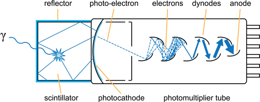
Figure 7. Schematic cross-section of a scintillation crystal coupled to a photomultiplier tube. See text for explanation.
Download figure:
Standard image High-resolution imageOnly a fraction of the photons incident on the photocathode contribute to the anode signal. This fraction has been defined as the PDE  in chapter 2. The PDE equals the product of the quantum efficiency (QE) of the photocathode and the photoelectron collection efficiency of the first dynode (i.e. an electrode that functions as an electron multiplier through secondary emission). The QE is the probability that a photon incident on the photocathode leads to the emission of an electron. The probability that this photoelectron gives rise to a signal at the PMT anode equals the photoelectron collection efficiency of the first dynode. It is common practice, however, to loosely refer to the PDE of a vacuum PM as the 'QE of the photomultiplier.' PMTs with a standard bialkali photocathode typically have a QE of ∼25% around 400 nm, but PMTs with a so-called super-bialkali or ultra-bialkali photocathode may reach a QE of up to ∼35% or ∼43%, respectively (Kapusta et al
2007, Nakamura et al
2010). The red curve in figure 5 shows the QE curve of a PMT with an ultra-bialkali photocathode.
in chapter 2. The PDE equals the product of the quantum efficiency (QE) of the photocathode and the photoelectron collection efficiency of the first dynode (i.e. an electrode that functions as an electron multiplier through secondary emission). The QE is the probability that a photon incident on the photocathode leads to the emission of an electron. The probability that this photoelectron gives rise to a signal at the PMT anode equals the photoelectron collection efficiency of the first dynode. It is common practice, however, to loosely refer to the PDE of a vacuum PM as the 'QE of the photomultiplier.' PMTs with a standard bialkali photocathode typically have a QE of ∼25% around 400 nm, but PMTs with a so-called super-bialkali or ultra-bialkali photocathode may reach a QE of up to ∼35% or ∼43%, respectively (Kapusta et al
2007, Nakamura et al
2010). The red curve in figure 5 shows the QE curve of a PMT with an ultra-bialkali photocathode.
The time between emission at the photocathode and arrival at the first dynode is not the same for all photoelectrons. Differences may occur due to differences in the path lengths as well as the initial speeds of the photoelectrons. These are the major contributions to the TTS of typical PMTs. Additional time dispersion may arise due to fluctuations in the multiplication process. The statistics behind these processes have been studied in depth in the 1960s and 70s and a brief overview of works from that period can be found in section 2.2. In particular, the theory by Hyman (1965) has found widespread use in scintillation detector research and it has been shown that it is a special case of the Seifert model developed more recently (see section 4.3.4).
PMT manufacturers have developed a variety of PMTs optimized for fast timing applications. The first commercial PET scanners utilizing LSO:Ce crystals did not use such fast PMTs, as the systems were optimized for spatial and energy resolution rather than timing. The CRT of these systems was limited to about 1.2 ns (Conti et al 2005). This could be improved by a factor of about two by introducing fast-timing PMTs, along with improved electronics and signal processing (Surti et al 2007, Bettinardi et al 2011, Jakoby et al 2011). Fast-timing PMTs are optimized so that photoelectrons emitted from different points on the photocathode arrive at the first dynode simultaneously as much as possible. This is typically achieved using a plano-concave window (as schematically indicated in figure 7), to reduce path length variations, and accelerator electrodes between the photocathode and first dynode, to boost the electron speed (Wright 2017). The use of a linear-focused dynode structure minimizes the dispersion during the subsequent multiplication stage. A 'screening grid' placed in front of the anode can help to improve the rise time of the anode pulse (Moszynski et al 2016b). While the TTS of classic PM tubes is in the order of ∼ns, fast PMTs may have TTS values better than 200 ps FWHM (Moszyński et al 2006, Szczȩśniak et al 2009, Wiener et al 2010).
The way in which the anode pulse is processed constitutes the final contribution to the time resolution. In general, the electrical properties of PMTs are quite favorable for obtaining good time resolution: they have high internal gain (∼106–108), low dark current, low capacitance (typically ∼10 pF), and the anode has the equivalent circuit of a current source with high bandwidth (∼GHz). The SER of a fast PMT typically has a FWHM in the order of a few nanoseconds. PMT front-end electronics are commonly designed to load the anode with a 50 Ω input resistance, sufficiently low to maintain high bandwidth while matching the characteristic impedance of coaxial cables. If a LED is used to derive a timestamp from the anode pulse, the best time resolution is obtained if the threshold is set at a specific fraction, typically between 0.1 and 0.3, of the average pulse height (Knoll 2010). Such a relatively high threshold makes the time pickoff susceptible to pulse height variation, which inevitably occurs due to the finite energy resolution of the scintillator and the gain dispersion of the PMT. A CFD remedies this problem by triggering on a fixed fraction of the actual pulse height (Gedcke and Mcdonald 1968, Bengtson and Moszynski 1970, Lynch 1975).
A variety of clinical whole-body TOF-PET scanners based on PMTs and L(Y)SO:Ce crystals are and/or have been commercialized, e.g. (Surti et al 2007, Bettinardi et al 2011, Jakoby et al 2011, Kolthammer et al 2014, Kaneta et al 2017, Huo et al 2018). These systems all have a CRT > 400 ps FWHM. However, much better CRTs have been achieved in benchtop experiments using small scintillation crystals coupled one-to-one to fast PMTs. For example, Szczesniak et al (2010) obtained CRTs of 235–245 ps FWHM using 10 mm × 10 mm × 5 mm LSO:Ce crystals coupled to a fast-timing PMT with a QE of 34%, a measured TTS of 520 ± 25 ps FWHM, and a screening grid at the anode (Szczȩśniak et al 2009). Using equally sized LSO:Ce crystals with different concentrations of Ca co-doping coupled to the same PMT, they achieved CRTs of 192–205 ps FWHM.
Wiener et al (2010) reached a CRT of ∼230 ps FWHM with 4 mm × 4 mm × 5 mm LYSO:Ce crystals coupled to a fast PMT with a QE of 0.18 and a TTS of 160 ps FWHM. Comparison of this result with those of Szczesniak et al (2010) confirms the theoretical prediction that  and
and  both are important for good timing. Wiener et al (2010) furthermore performed tests with 4 mm × 4 mm × 5 mm LaBr3:Ce and CeBr3 crystals coupled to the same fast PMT. They achieved CRTs of ∼100 ps FWHM, which may be compared with the CRT of 375 ps FWHM of the LaBr3:Ce(5%) whole-body TOF-PET scanner built by the same group (Daube-Witherspoon et al
2010).
both are important for good timing. Wiener et al (2010) furthermore performed tests with 4 mm × 4 mm × 5 mm LaBr3:Ce and CeBr3 crystals coupled to the same fast PMT. They achieved CRTs of ∼100 ps FWHM, which may be compared with the CRT of 375 ps FWHM of the LaBr3:Ce(5%) whole-body TOF-PET scanner built by the same group (Daube-Witherspoon et al
2010).
The main causes of difference between the benchtop results and the CRT values obtained in TOF-PET systems include the increased crystal length, the use of less expensive PMTs with inferior timing properties, and deterioration of time information due to the use of light sharing. Additional factors may play a role in some systems, such as baseline instability at high count rates, or the use of LEDs instead of CFDs for time pickoff.
4.2.2. Other vacuum photomultipliers
The relatively large TTS of classic PM tubes is a direct consequence of the relatively long distances (∼cm) traversed by the (photo-) electrons. Another disadvantage of the large size of these devices is that light-sharing techniques must be used to read out the arrays of crystals typically used in PET systems. Both factors limit the CRT that can be achieved with such detectors.
Other types of vacuum photomultiplier exist, some of which offer prospects for better timing without sacrificing spatial resolution. One example is the multi-anode PMT (MA-PMT), which collects the amplified current on multiple anodes that can be read out individually. MA-PMTs typically have a square cross section and may be subdivided into e.g. 8 × 8 or 16 × 16 channels that (if we neglect crosstalk) act as independent PMTs. Of particular interest are MA-PMTs equipped with metal-channel dynodes. These consist of parallel columns of micro-machined dynodes, stacked in close proximity to each other to achieve short and consistent electron path lengths. MA-PMTs may have TTS values comparable to those of fast PMTs. Moreover, the multi-anode design reduces the need to use light sharing and, therefore, offers better options for the simultaneous optimization of spatial and time resolution. However, the gain non-uniformity of MA-PMTs can be substantial.
Krishnamoorthy et al (2014) performed experiments using a 49 mm × 49 mm MA-PMT with 8 × 8 anode pads, a QE of ∼25%, and a TTS of ∼0.4 ns. Time pickoff was performed on a common dynode signal using a rise-time-compensated fast-timing discriminator. They obtained a CRT of ∼300 ps FWHM with single, 1.5 mm × 1.5 mm × 12 mm LYSO:Ce crystals. Ko and Lee (2015) tested 23 mm × 23 mm metal-channel MA-PMTs equipped with super-bialkali and ultra-bialkali photocathodes. The common timing signal from the 12th dynodes was amplified and fed into a 12 bit, 5 Gs s−1 waveform digitizer. A CRT of ∼250 ps FWHM was obtained with 4 mm × 4 mm × 10 mm LYSO:Ce crystals coupled to the MA-PMT with ultra-bialkali photocathode (QE ∼37% at 420 nm, TTS ∼0.34 ns).
Another type of dynode with good timing properties is the so-called microchannel plate (MCP). It typically consists of a two-dimensional array of glass capillaries (the 'channels'), each with an inner diameter in the order of ∼10 μm and with the inner wall processed to have the proper resistance and secondary emissive properties. A voltage gradient is applied along the length of the capillaries, so that each channel acts as an independent electron multiplier. The length of the channels typically is in the order of ∼1 mm. By placing the MCP at a similarly short distance from a flat photocathode, the electron path lengths are kept as short as possible. A multi-channel arrangement similar to the MA-MPT is possible, by placing a two-dimensional array of anode pads behind the MCP. As in MA-PMTs, gain non-uniformity can be an issue in such MA-MCP-PMTs. The TTS of a small, single-anode MCP-PMT can be as low as ∼25 ps FWHM. A disadvantage is that part of the photoelectrons backscatter on the front surface of the MCP. These typically show up as delayed peaks in the anode pulses of MCP-PMTs exposed to short light pulses. Thus, they still contribute to the integral charge collected, but the time information carried by the backscattered photoelectrons is mostly lost. The fraction of electrons that backscatter is determined by the ratio of the open area to the total effective area of the MCP.
Choong (2010) tested a commercial MA-MCP-PMT with a photosensitive area of 53 mm × 53 mm and 8 × 8 anode pads. The TTS was measured to be 120 ps FWHM, while the SPTS showed the expected tail due to backscattered photoelectrons. Using a 4 mm × 4 mm × 10 mm LSO:Ce crystal coupled at different positions to the MCP-PMT, he found an average time resolution of 252 ± 7 ps FWHM in the central region, which degraded to 280 ± 9 ps FWHM for edge pixels and 316 ± 15 ps FWHM for corner pixels. Kim et al (2012) performed measurements with 3 mm × 3 mm × 10 mm LYSO:Ce crystals coupled to the center of similar commercial MCP-PMTs read out with transmission-line strips and 5 Gs s−1 waveform digitizers. They reported a CRT of 309 ps FWHM. The large-area picosecond photodetector collaboration recently developed a 20 cm × 20 cm MCP-PMT with position-sensitive readout using transmission-line strips (Adams et al 2015). Achieving good performance while lowering the costs of manufacturing per unit area is a key objective of this project. The TTS, measured using a ∼1 mm diameter laser beam scanned over a 7 mm × 7 mm area, was reported to be 120 ± 14 ps FWHM.
A novel type of dynode currently under development is the so-called tynode (van der Graaf et al 2017), i.e. a transmission dynode in the form of planar, ultra-thin, electron-emitting membranes manufactured in microelectromechanical systems (MEMS) technology. The idea is to stack several of these membranes on top of each other, with a planar photocathode placed directly above the stack. Electrons impinging on the top surface of the top tynode cause the emission of several electrons from the bottom surface, which are accelerated towards the next tynode, and so on. The stack can be mounted onto a pixel chip, resulting in a planar PMT with a thickness in the order of 1 mm. High 2D position resolution and potentially excellent TTS are expected, due to the very short electron path lengths. It has been estimated that a transmission secondary electron yield (TSEY) >4 is required to make this concept practical (Bilevych et al 2016). Recently, TSEY values of up to 5.5 have been measured (Prodanovic 2019).
4.2.3. SPTR versus TTS
Manufacturers of single-photon sensors specify the temporal properties of their devices using several parameters. These can be subdivided into parameters characterizing the single-photon timing performance and the shape of the output pulses. For example, PMT manufacturers commonly use the TTS as a measure of timing performance and furthermore report the rise time, fall time, and FWHM of the SER. A reasonably fast PMT might e.g. have a TTS of ∼0.5 ns, a SER rise time of ∼1 ns, and a fall time that is typically ∼3 times longer. Knowledge of both the TTS and the SER is needed when modeling the signal formation of a scintillator-PMT combination in detail, e.g. when using the models of Hyman (1965) or Seifert et al (2012c).
Manufacturers of solid-state single-photon sensors typically use the SPTR as a measure of timing performance. What is the relationship between SPTR and TTS? Let us examine how the TTS is measured in practice. The photocathode is uniformly illuminated by a pulsed laser, making sure that no more than one photon hits the photocathode per pulse. The PMT output is fed into a time-pickoff circuit (e.g. a CFD) and a histogram of the time differences between the laser pulses and the corresponding PMT anode pulses is recorded. The TTS is quoted as the FWHM (or standard deviation) of the measured time difference spectrum. Now, let us examine two extreme cases. First, we assume that the anode pulses have infinitesimal width. In this case, the width of measured histogram is determined by the variation in signal transit times only. In the second case, we assume that there is no TTS, but the SER has a finite rise and fall time. The width of the histogram is then determined by the slope-over-noise ratio of the SER at the point where it crosses the discriminator threshold (Knoll 2010). The slope at threshold crossing is determined by the shape of the SER and the PMT gain, while the noise is primarily determined by the photocathode dark current (magnified by the same gain as the signal) and the electron multiplication statistics. (Note that external contributions, e.g. due to laser jitter, may be corrected for by measuring the instrument response function (IRF) of the measurement setup.) In practice, TTS measurements are somewhere in between these two extremes. In other words, the measured time difference spectrum includes contributions from TTS as well as noise. Thus, it completely characterizes the SPTR of a vacuum PMT. Indeed, the measured TTS is equal to the SPTR defined in chapter 2, provided that the light source illuminates the photocathode uniformly.
The reason that the term TTS, rather than SPTR, is commonly used for vacuum photomultipliers is of historic origin and reflects the fact that the spread in the transit times of the photoelectrons to the first dynode constitutes the largest contribution to the SPTR of classic PM tubes. As this contribution is greatly reduced in some of the more novel vacuum photomultiplier technologies, it may be appropriate to start using the term SPTR for such devices.
4.3. Silicon photomultipliers
The interest to replace PMTs in PET detectors by semiconductor photosensors exists for several decades already. Advantages of solid-state light sensors over PMTs include a high PDE, low-voltage operation, small size, flexibility in sensor geometric design, ruggedness, and unperturbed performance in strong magnetic fields. These properties enable the development of new detector designs aimed at, for example, compactness, high resolution, DOI capability, and MRI compatibility.
PET detectors based on (p–i–n) photodiodes and avalanche photodiodes (APDs) were explored by various authors in the 1990s and early 2000s (Budinger 1998, Humm et al 2003, Lewellen 2008, Peng and Levin 2010). A main limitation of the photodiode is its lack of internal amplification. In this respect, APDs represented a significant improvement. APDs operate at a large reverse bias (typically several hundreds of volts), giving rise to a high electric field strength in the depletion region of the diode. Charge carriers created upon the absorption of a scintillation photon are accelerated in this field and produce additional ionizations, resulting in the creation of an avalanche. A proportional gain in the order of 102–103 can be achieved in this way. Moreover, the PDE of an APD can be higher than 90%.
APDs have found application in (prototype) PET and PET/MRI systems for e.g. small-animal, organ-specific, and plant imaging (Auffray et al 2006, Spanoudaki et al 2006, Catana et al 2008, Judenhofer et al 2008, Bergeron et al 2009, Bugalho et al 2009, Beer et al 2010, Herzog et al 2011, Schulz et al 2011, Kolb et al 2012). Moreover, they were used in the first commercial whole-body clinical PET/MRI system (Delso et al 2011). Unfortunately, the response of APDs tends to be relatively slow (typically exhibiting a ∼10 ns signal rise time), due to their relatively large diode capacitance. This makes it difficult to achieve a time resolution sufficiently good for TOF-PET using APDs.
A more recent development in the field of solid-state photosensors is the so-called silicon photomultiplier. Figure 8 shows examples of a single SiPM (left) and a 4 × 4 SiPM array, in which each of the individual SiPMs (also called pixels) can be read out individually (right). These devices are of great interest to TOF-PET as they offer a high PDE, a high internal gain, and a relatively fast response. SiPMs can be fabricated using complementary metal-oxide-semiconductor (CMOS) technology, enabling low-cost production when manufacturing large quantities. SiPMs operate at bias voltages of several tens of volt only. The history of development and the principles of operation of (analog) SiPMs have been reviewed by many authors, e.g. (Renker 2006, Renker and Lorenz 2009, Roncali and Cherry 2011, Donati and Tambosso 2014, Bisogni and Morrocchi 2016, Acerbi and Gundacker 2019, Piemonte and Gola 2019, Gundacker and Heering 2020, Vinogradov and Popova 2020). In what follows, the focus will therefore be on timing aspects.

Figure 8. Photographs of (left) a 6 mm × 6 mm single SiPM chip (Broadcom AFBR-S4N66C013) and (right) a SiPM array comprising 4 × 4 SiPMs ('pixels') of 4 mm × 4 mm each (Broadcom AFBR-S4N44P163). Dead space between the SiPM chips is minimized due to the use of through-silicon via (TSV) technology; the second image from the left shows the soldering balls on the backside of the 6 mm × 6 mm chip. Reproduced with permission from Broadcom Inc.
Download figure:
Standard image High-resolution image4.3.1. SiPM topology and principle of operation
The presently most common implementation of the SiPM comprises a large number (typically 102 –105) of APDs operated in Geiger mode and aligned in a two-dimensional array as shown in figure 9 (left). These elements are commonly referred to as single-photon avalanche diodes or microcells. The SPADs are electrically connected in parallel as shown in figure 9 (right), such that the SiPM output current equals the sum of the currents produced by the fired SPADs. Devices with this topology are sometimes called analog SiPMs to distinguish them from their digital counterparts, which are discussed in section 4.3.6.
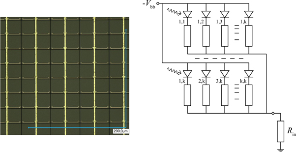
Figure 9. Left: microscope image of the front surface of a Broadcom AFBR-S4N44C013 SiPM, showing the two-dimensional array of 30 μm × 30 μm SPADs and metallization (courtesy of Broadcom Inc.). Right: parallel electrical connection of many SPADs in a SiPM; the symbol  denotes the bias voltage and
  is the input resistance of the readout circuit. Reprinted from Schaart (2020) with permission from Springer.
Download figure:
Standard image High-resolution imageFigure 10 shows an example of the cross-sectional structure of the SPADs in a SiPM. They are operated at a reverse bias voltage  that exceeds the breakdown voltage
  by a few volts. In this regime a triggered avalanche becomes self-sustaining and continues until it is quenched. In most SiPMs this is achieved using a quench resistor placed in series with the diode, as indicated in figure 9 (right).
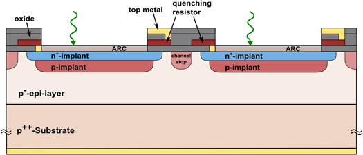
Figure 10. Schematic cross-section of two adjacent SPADs of a SiPM manufactured in n-on-p technology. Reprinted from Acerbi et al (2014b) with permission from the authors and IEEE.
Download figure:
Standard image High-resolution imageThe gain of a SPAD (typically in the order of 105–107) is much higher than that of an APD that is operated in proportional mode. The total charge released in a discharge is independent of the number of initial charge carriers (Popova et al 2015). Thus, a SPAD can detect one photon at a time; it is indeed a single-photon counter. The massive parallel connection of many SPADs in a SiPM allows for a nearly proportional response if the light intensity is sufficiently low, i.e. if there is a negligible probability that more than one photon will hit any SPAD during the time it takes to fully recharge.
SiPMs have a number of non-idealities that can affect the performance of a PET detector. The review papers cited in the first paragraph of this section provide useful information and references on these effects, therefore only some essential points are highlighted here. For example, the gain is a function of the voltage-over-breakdown  where
where  depends on temperature. To achieve stable gain, the SiPM temperature may need to be controlled and/or
  may need to be adjusted continuously to the device temperature. Furthermore, dark counts occur due to the triggering of avalanches by thermally generated electron–hole (e–h) pairs and field-assisted generation of free electrons. Thermal generation is often dominant at room temperature and the resulting dark count rate (DCR) increases with temperature. The DCR of a SiPM furthermore increases with increasing
  and device area. Room-temperature DCR values of commercial SiPMs have decreased from the ∼MHz mm−2 level to less than 100 kHz mm−2 for some devices. Fortunately, because of the relatively short (<1 μs) signal integration times used in PET, the relative contribution of dark counts to the total integrated charge per event can usually be kept small.
A fundamental non-ideality of any SiPM is that its response is inherently non-proportional due to the combined effects of saturation, afterpulsing, and crosstalk. The response can be expressed as:

where  is the equivalent number of fired SPADs, defined as the ratio of the total signal charge and the charge due to a single fired SPAD, while
  is the number of primary triggers, i.e. the number of photons that trigger a discharge in one of the SPADs. Saturation occurs when SPADs are triggered by more than one photon during their recharge time. Afterpulses are due to charge carriers trapped during a Geiger discharge and released at a later time, triggering a new avalanche. The SPAD recharge time, overvoltage, and temperature influence the afterpulsing probability, which typically has a value in the order of 0.1%–10% at room temperature. Crosstalk between SPADs is caused by the optical photons produced within an avalanche, which may trigger discharges in neighboring SPADs. The crosstalk probability may be in the order of 1%–20% and is influenced by the structure of the device and the overvoltage.
A simple model of the influence of saturation on the response of SiPMs is applicable to instantaneous light pulses only and furthermore assumes that crosstalk, afterpulsing, and dark counts are absent. The lower limit of the SiPM response is reached under these conditions. For a SiPM that consists of  SPADs, this lower limit equals:

This simple model may be insufficient if the influences of crosstalk and afterpulsing are not negligible and/or the light pulse is not instantaneous, such as in a PET scintillation detector. An analytical model of the SiPM response, applicable to exponentially decaying as well as instantaneous light pulses, has been developed by Van Dam et al (2010). Other authors have developed Monte Carlo models of SiPMs coupled to scintillators, e.g. Pulko et al (2012). Furthermore, Jha et al (2013) developed a comprehensive but computationally efficient, combined discrete-time discrete-event Monte Carlo model that can be used to simulate not only the expectation value, but also the variance of the SiPM response to light pulses of any shape.
4.3.2. Single-SPAD response of analog SiPMs
To understand the timing properties of a SiPM, it is useful to first consider the signal produced when a discharge occurs in one of its SPADs, the so-called single-SPAD response (SSR). Figure 11 shows an equivalent circuit commonly used to simulate the SSR of SiPMs. The active SPAD comprises a reverse-biased photodiode with capacitance  This diode is placed in series with a quench resistor
  that has a parasitic or intentional parallel capacitance
  The
The  remaining SPADs are represented by the corresponding quantities in the 'passive' section of the equivalent circuit. The quantity
  denotes the parasitic capacitance per microcell, hence
  equals the total parasitic capacitance of the SiPM. This term mainly represents the capacitance of the metal grid, while the capacitance of the bonding pads can be included as well.
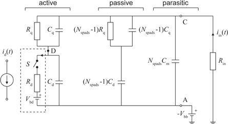
Figure 11. Equivalent circuit used to model the firing of a single SPAD in a SiPM. The branch within the dashed box is sometimes replaced by a current source  See text for explanation of the other symbols.
Download figure:
Standard image High-resolution imageThe closing of the switch S in the active SPAD represents the triggering of a discharge by a photon. At the moment  the switch is closed, the difference between
  and
and  i.e.
i.e.  instantly appears across
  which represents the internal resistance of the diode space-charge region. The resulting current through
  can be described according to Marano et al (2014):

where  and:
and:

The current  causes the voltage at the node D between the diode and the quench resistor to decrease exponentially from the bias voltage
  to
to  (relative to the anode). To hold the cathode at
  the bias supply must deliver a current
  that is proportional to
  and passes through the input resistance
  In the ideal case in which the measured signal is not affected by bandwidth or slew-rate limitations, its rise-time constant therefore equals
  which can be in the range of tens of picoseconds.
The switch remains closed until  reaches the threshold value
  below which the avalanche is no longer self-sustaining. At that point, the switch opens to mimic the quenching of the avalanche. Since
  the total charge that has flown through the diode can be approximated by:

The SiPM gain thus equals  with
with  the unit electron charge.
After the switch has been re-opened, the SPAD will return to its initial state and, consequently,  will return to zero. This process is governed by two time constants, corresponding with the two real poles of the small-signal transfer function of the circuit shown in figure 11. Thus, the SSR can be modeled as (Marano et al
2014):
will return to zero. This process is governed by two time constants, corresponding with the two real poles of the small-signal transfer function of the circuit shown in figure 11. Thus, the SSR can be modeled as (Marano et al
2014):

where 
 and
and  are positive constants, defined such that the integral of the term between brackets equals unity.
The SSR model given in equation (24) is characterized by a rise-time constant  and fall-time constants
  and
and  as illustrated in figure 12 (left). One often speaks of
  and
and  as the 'slow' and 'fast' components of the SSR, respectively (Dolinsky et al
2015). Note that
as the 'slow' and 'fast' components of the SSR, respectively (Dolinsky et al
2015). Note that  is also called the SiPM recharge- (or recovery-) time constant. The values of
  and
and  are given by:


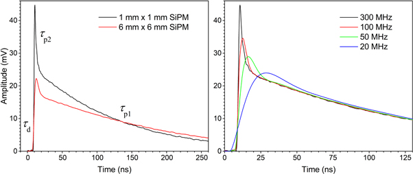
Figure 12. Left: single-SPAD response of 1 mm × 1 mm and 6 mm × 6 mm SiPMs, both measured at 300 MHz bandwidth. Right: SSR of a 1 mm × 1 mm SiPM measured at different bandwidths. The SiPMs were all based on the same 40 μm SPAD and all measurements were performed at 0 °C and  = 4 V. Data taken from Acerbi and Gundacker (2019) with permission from the authors.
Download figure:
Standard image High-resolution imageIn the derivation of equations (25) and (26), it has been assumed that  but, in contrast with Marano et al (2014), not necessarily
The recharge-time constant  reaches a minimum value of
  for
for  Thus,
Thus,  parameterizes the charging of
  (and the corresponding discharging of
  ) through
  Typical values of
  are in the order of ∼10 to ∼100 ns. A small value of
  is beneficial for obtaining good time resolution with scintillators, as will be discussed in section 4.3.4.
The fast time constant  in first-order approximation is proportional to
  Typical values of
  are in the order of nanoseconds. In practice, the fast component of the SSR is only visible if the readout circuit has sufficiently high bandwidth and
  is kept sufficiently small. It is noted that the fraction of the total charge
  contained within the fast component increases if the ratio
  becomes larger. Remembering that
  and
and  are proportional to
  (equations (22) and (23), respectively), it follows that increasing
  for a given value of
  can improve the timing performance of a SiPM design.
Furthermore, equations (25) and (26) show that both  and
and  decrease if
  is made smaller. Since
  and
and  are determined by the SPAD design only (equations (22) and (23), respectively), it follows that the initial slope of the SSR is highest for small values of
  Indeed, the measured SSR curves of a 1 mm2 and a 36 mm2 SiPM based on the same SPAD in figure 12 (left) illustrate that small SiPMs are favorable for detecting single photons with high time resolution.
Several variations of the SiPM equivalent circuit shown in figure 11 exist. The use of the switch S for modeling the triggering of a discharge was proposed by Seifert et al (2009), in accordance with the elementary work from Haitz (1964) and the single-SPAD model from Cova et al (1996). Several authors have adopted this approach (Marano et al
2013, Acerbi and Gundacker 2019) and/or extended it (Villa et al
2015). Marano et al (2014) facilitated the mathematical analysis of the circuit by substituting the series connection of 
 and S by the current source
  defined in equation (21), as indicated by the dashed box in figure 11. The results of such analysis have been summarized above. Jha et al (2013) derived an alternative analytical expression of the SSR, replacing equation (21) by a double-exponential function to account for the fact that the build-up of the avalanche takes a finite amount of time. In contrast, simply modeling
  as a very short current pulse can be sufficient when accurate modeling of the rising edge of the SSR is less important (Corsi et al
2007, Condorelli et al
2011, Licciulli and Marzocca 2016).
as a very short current pulse can be sufficient when accurate modeling of the rising edge of the SSR is less important (Corsi et al
2007, Condorelli et al
2011, Licciulli and Marzocca 2016).
4.3.3. Single-photon timing properties of analog SiPMs
The high internal gain and relatively fast response of SiPMs (section 4.3.2) make them attractive for use in TOF-PET detectors. As with any photosensor, this requires that the first scintillation photons have a high probability of being detected. In principle, efficient crystal-sensor coupling is facilitated by the high refractive index of silicon, e.g.  at 420 nm, the peak emission wavelength of L(Y)SO:Ce. However, the scintillator is usually not in direct contact with Si; besides the fact that a surface passivation layer is required for good sensor performance, most SiPM are mechanically protected using e.g. an epoxy or glass cover, typically with a refractive index of about ∼1.5. Thus, crystal-sensor coupling issues similar to the case of vacuum photomultipliers commonly arise (section 4.2.1). In fact, the small size of SiPMs can make it even more challenging to avoid light loss. For example, bond-wire trenches or other gaps can act as light sinks, especially in SiPM arrays assembled from discrete SiPMs. The introduction of arrays with very small inter-SiPM gaps, based on four-side-buttable sensor chips in TSV packages, is an important improvement in this regard.
The PDE  of a SiPM at sparse illumination conditions is often described as the product of its so-called fill factor (FF), the QE of the SPADs, and the trigger probability
  The FF simply equals the sum of the SPAD active areas divided by the total device area. SiPMs typically have a FF in the range of 20%–80%. The QE of a SPAD equals the probability that a photon incident on its active area creates an e–h pair capable of initiating an avalanche, while
  is the probability that such an e–h pair triggers a pulse of adequate gain to be counted (Dautet et al
1993). The trigger probability depends on the position at which the primary e–h pair is generated, as well as the electric field shape and strength. It increases with increasing
is the probability that such an e–h pair triggers a pulse of adequate gain to be counted (Dautet et al
1993). The trigger probability depends on the position at which the primary e–h pair is generated, as well as the electric field shape and strength. It increases with increasing  The QE may reach values above 90% within a limited range of wavelengths if proper antireflection coatings are applied. The PDE can thus be tuned to the scintillator emission spectrum by adapting the SPAD design, see figure 5 for an example. Below about ∼400 nm, most photons are absorbed in a shallow layer of Si (<0.1 μm) and special processing of the SPADs is necessary to avoid that the resulting e–h pairs recombine at the surface. SiPMs optimized for vacuum ultraviolet wavelengths have thus been developed (Sato et al
2013). Conversely, SPADs have to be made relatively thick for the efficient detection of red light. Above about ∼800 nm, the absorption coefficient of Si becomes so low that photons may penetrate even thick SPADs without being absorbed.
The QE may reach values above 90% within a limited range of wavelengths if proper antireflection coatings are applied. The PDE can thus be tuned to the scintillator emission spectrum by adapting the SPAD design, see figure 5 for an example. Below about ∼400 nm, most photons are absorbed in a shallow layer of Si (<0.1 μm) and special processing of the SPADs is necessary to avoid that the resulting e–h pairs recombine at the surface. SiPMs optimized for vacuum ultraviolet wavelengths have thus been developed (Sato et al
2013). Conversely, SPADs have to be made relatively thick for the efficient detection of red light. Above about ∼800 nm, the absorption coefficient of Si becomes so low that photons may penetrate even thick SPADs without being absorbed.
SiPMs are currently available with PDE values of about ∼60% at 420 nm (Gola et al 2019), significantly exceeding those of state-of-the-art vacuum photomultipliers. It is noted that the accurate measurement of SiPM PDE curves is not trivial and that results may depend on the method used. In particular, care should be taken to eliminate the influence of crosstalk and afterpulsing; these effects do not contribute to the efficiency of the sensor but represent sources of (correlated) noise.
Before discussing the SPTR of a SiPM, it is instructive to consider the SPTR of a single SPAD. Figure 13 shows measured examples of the SPTS of a 20 μm SPAD at different  The SPTS is often described as consisting of a Gaussian part (indicated by the dashed line for
  = 6.5 V) and an exponential tail. The tail is caused by charge carriers photogenerated in the neutral region beneath the active junction, which reach the multiplication region by diffusion (Ripamonti and Cova 1985). The diffusion tail can be suppressed through proper modification of the SPAD design (Ghioni et al
2007), as illustrated in figure 13. In that case, the SPTR is primarily determined by the FWHM of the Gaussian part, which is due to photons absorbed in the depletion region. The width of the Gaussian part is determined by several factors (Lacaita et al
1993, Spinelli and Lacaita 1997, Sciacca et al
2003). These include (1) the drifting of the photo-generated charge carriers to the multiplication region, resulting in a time spread in the order of ∼10 ps per μm thickness of the depletion layer; (2) fluctuations in the subsequent development of the avalanche, determined by longitudinal avalanche multiplication statistics and lateral spreading of the avalanche (Knoetig et al
2014, Popova et al
2015); and (3) non-uniformity of the electric field across the SPAD active area, giving rise to different avalanche build-up characteristics near the border of the SPAD and a worsening of the SPTR value if the whole SPAD is illuminated compared to the center region only (Acerbi et al
2014a, Nemallapudi et al
2016a).
= 6.5 V) and an exponential tail. The tail is caused by charge carriers photogenerated in the neutral region beneath the active junction, which reach the multiplication region by diffusion (Ripamonti and Cova 1985). The diffusion tail can be suppressed through proper modification of the SPAD design (Ghioni et al
2007), as illustrated in figure 13. In that case, the SPTR is primarily determined by the FWHM of the Gaussian part, which is due to photons absorbed in the depletion region. The width of the Gaussian part is determined by several factors (Lacaita et al
1993, Spinelli and Lacaita 1997, Sciacca et al
2003). These include (1) the drifting of the photo-generated charge carriers to the multiplication region, resulting in a time spread in the order of ∼10 ps per μm thickness of the depletion layer; (2) fluctuations in the subsequent development of the avalanche, determined by longitudinal avalanche multiplication statistics and lateral spreading of the avalanche (Knoetig et al
2014, Popova et al
2015); and (3) non-uniformity of the electric field across the SPAD active area, giving rise to different avalanche build-up characteristics near the border of the SPAD and a worsening of the SPTR value if the whole SPAD is illuminated compared to the center region only (Acerbi et al
2014a, Nemallapudi et al
2016a).
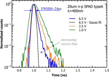
Figure 13. Single-photon timing spectra of a single 20 μm SPAD, for  = 1.0 V (green curve), 2.5 V (orange curve), and 6.5 V (blue curve). The dashed curve represents a Gaussian fit to the SPTS measured at 6.5 V. © 2014 IEEE. Reprinted with permission, from Acerbi et al (2014a).
Download figure:
Standard image High-resolution imageThe SPTR of a SPAD improves with increasing  as illustrated in figure 13. Values in the range of 20–50 ps FHWM are commonly achieved today (Cova et al
1989, Ghioni et al
2007, Acerbi et al
2014a, Brunner et al
2016, Nemallapudi et al
2016a, Cates et al
2018, Nolet et al
2018). It is noted that there may be a trade-off between PDE and SPTR, especially at longer wavelengths; thick SPADs are required for the efficient detection of red light, which comes at the expense of an increased spread in charge carrier drift times (Buller and Collins 2010). It is much easier to achieve good PDE as well as SPTR values in the blue region.
as illustrated in figure 13. Values in the range of 20–50 ps FHWM are commonly achieved today (Cova et al
1989, Ghioni et al
2007, Acerbi et al
2014a, Brunner et al
2016, Nemallapudi et al
2016a, Cates et al
2018, Nolet et al
2018). It is noted that there may be a trade-off between PDE and SPTR, especially at longer wavelengths; thick SPADs are required for the efficient detection of red light, which comes at the expense of an increased spread in charge carrier drift times (Buller and Collins 2010). It is much easier to achieve good PDE as well as SPTR values in the blue region.
In first-order approximation, one might expect that the SPTR of a SiPM that consists of  parallel-connected SPADs is equal to that of a single SPAD of the same type, since the physics of e–h pair creation and avalanche multiplication are the same in each SPAD. In practice, several factors deteriorate the SPTR of a SiPM compared to that of a single SPAD. These include differences between individual SPADs as well as phenomena that occur at the level of the device as a whole.
For example, slight differences in the breakdown voltages of different SPADs may give rise to gain dispersion. Furthermore, a spread in the quench resistor values may cause the pulse shapes (SSR time constants) of different SPADs to be different, see equations (22), (25), and (26). Different lengths and impedances of the metal traces that connect the SPADs to the SiPM output pad may cause additional pulse shape variation as well as a spread in the pulse propagation times; for SiPMs with areas between 9 mm2 and 36 mm2, the corresponding skews were found to range from several tens to several hundreds of ps, depending on the sensor area and metallization layout (Seifert et al 2009, Nagano et al 2012, Acerbi et al 2015, Dolinsky et al 2015). Typically, these skews give rise to a non-Gaussian contribution to the SPTS. It is noted that this contribution is sometimes referred to as 'SiPM TTS.' In this review, however, the term TTS is used exclusively in accordance with section 4.2.3, i.e. as a historic term for the quantity nowadays referred to as SPTR, which includes all sources of single-photon time spread.
Spurious pulses are another phenomenon that worsen the measured SPTR of a SiPM compared to a single SPAD. The DCR, for example, is proportional to  Dark counts have the same characteristics as photon-triggered SPAD pulses and occur at random times, hence they give rise to a uniform background in a SPTR experiment. More importantly, the time at which a photon-triggered SPAD pulse crosses a given threshold changes if the pulse happens to sit on the long tail of a preceding dark count. One might think of the corresponding time spread as resulting from low-frequency noise or baseline variation. It is noted that dark counts also produce crosstalk and afterpulses. The DCR as well as the crosstalk and afterpulsing probabilities increase with increasing
  So, while the SPTR of a single SPAD tends to improve with increasing
  in a SiPM this is counteracted by increasing baseline variation due to spurious pulses. Thus, some form of baseline restoration is often required to achieve optimum SPTR with SiPMs (see also section 4.3.5).
Finally, a high bandwidth readout circuit is required to preserve the rising edge and fast component of the SSR of a SiPM (equation (24)). Figure 12 (right) shows examples of SSR measurements performed at different bandwidths. Marano et al (2016) derived an analytical expression of the SSR of a SiPM coupled to readout electronics, in which  and
and  defined as in figure 14, are used to model the −3 dB cut-off frequency of the readout circuit in the dominant-pole approximation.

Figure 14. Small-signal equivalent circuit of a SiPM connected to a preamplifier with transconductance  input resistance
  output resistance
  and output capacitance
  The voltage gain and –3 dB cut-off frequency of the preamplifier are given by
  and
and  respectively. See text for explanation of the other symbols.
Download figure:
Standard image High-resolution imageRather than just the bandwidth of the readout electronics, however, the transient response of the entire SiPM-electronics chain should be considered (Huizenga et al
2012). In particular, the relatively high equivalent capacitance of a SiPM (up to ∼100 pF mm−2) forms an RC filter with the input resistance  of the readout circuit. Figure 15 illustrates the effect of
  on the SSR. Whereas
  equals ∼20 ns and the fast component is clearly visible at
  = 10 Ω (black curve), the recharge-time constant raises to ∼60 ns and the fast component almost disappears at a 'standard' input impedance of 50 Ω (green curve). Both effects reduce the initial slope of the SSR. As a result, the contribution of the electronic noise to the measured SPTR, determined by the slope-over-noise ratio (Knoll 2010), easily becomes significant, especially for larger SiPMs. Thus, it is important to use low-noise readout electronics and to make the input impedance of the readout circuit as low as possible at signal frequencies.
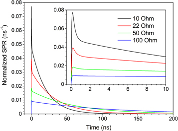
Figure 15. Single-SPAD response of a SiPM modeled according to Marano et al (2014) using  = 500 Ω,
  = 100 kΩ,
  = 100 pF,
  = 5 pF and
  = 104, for
  = 10 Ω (black curve), 22 Ω (red curve), 50 Ω (green curve), and 100 Ω (blue curve). The inset shows the first 10 ns of the same SSR curves. All plots were normalized to unit area under the curve.
Download figure:
Standard image High-resolution imageA factor easily overlooked in this context is the self-inductance of the wiring connections between the SiPM and the input of the front-end electronics, represented by  in figure 14. It appears that a series inductance of only a few nH can already deteriorate the initial slope of the SSR (Seifert et al
2009, Ciciriello et al
2013, Licciulli and Marzocca 2016, Calo et al
2019). Thus, the wiring connections should be designed such that
in figure 14. It appears that a series inductance of only a few nH can already deteriorate the initial slope of the SSR (Seifert et al
2009, Ciciriello et al
2013, Licciulli and Marzocca 2016, Calo et al
2019). Thus, the wiring connections should be designed such that  is kept as small as physically possible.
Cates et al (2018) recently published a study that nicely illustrates all of the above effects. They measured the SPTR of a single 40 μm SPAD as well as 1 mm × 1 mm, 3 mm × 3 mm, and 4 mm × 4 mm SiPMs based on the same SPAD, using a fast readout circuit that minimized the influence of electronic noise. After subtracting the remaining noise contribution, applying a correction for amplitude walk, and compensating for laser jitter, they obtained 'intrinsic' SPTR values of about ∼50 ps FWHM for both the single SPAD and the 1 mm × 1 mm SiPM. The corresponding values for the 3 mm × 3 mm and 4 mm × 4 mm SiPMs were larger (but still well below 100 ps FWHM), which was attributed to the larger differences in trace length in these devices. The authors also determined the SPTR of other brands of 3 mm × 3 mm SiPMs, obtaining values <150 ps FWHM in all cases and showing the importance of carefully optimizing the readout electronics when measuring the SPTR of large-area SiPMs.
4.3.4. Timing performance of SiPM-based scintillation detectors
The high PDE and excellent SPTR of contemporary SiPMs (section 4.3.3) make them attractive as an alternative to PMTs in TOF-PET detectors. Yet, achieving optimum timing performance from a SiPM-based scintillation detector imposes a number of challenges.
A first difference between SiPMs and PMTs concerns the shape and duration of their response to a single photon; whereas the SER of a fast PMT may have a FWHM of a few ns, the recharge-time constant  of a SiPM typically is one or two orders of magnitude larger. When the same scintillator is coupled to a PMT and a SiPM with equal gain, this implies that the initial slope of the SiPM-based detector signal will be much smaller, resulting in a greater sensitivity to electronic noise. For example, figure 16 (left) shows the SER of a typical fast-timing PMT (black curve) in comparison with the SSR of a SiPM. The SiPM has a recharge-time constant of ∼30 ns and a clearly visible fast component when loaded with
  = 5 Ω (green curve). When
  is raised to 50 Ω,
  increases to ∼66 ns and the fast component mostly disappears (red curve). Figure 16 (right) shows the corresponding detector output signals when these photosensors are coupled to a scintillator that decays exponentially with a time constant of 40 ns. Clearly, the SiPM-based detector offers a more favorable pulse when loaded with a low input impedance. Nevertheless, the steepest slope is obtained with the fast PMT in this example. Note that the optimum trigger level is much lower for the SiPM than for the PMT, both in absolute terms and as a fraction of the signal peak value.
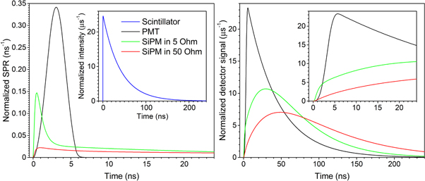
Figure 16. Left: SER of a fast PMT, modeled according to Hyman (1965) as a truncated Gaussian with a FWHM of 3 ns (black curve), and SSR of a SiPM, modeled according to Marano et al (2016) using  = 500 Ω,
  = 260 kΩ,
  = 80 pF,
  = 20 pF, and
  = 104, for
  = 5 Ω (green curve) and
  = 50 Ω (red curve). An electronic bandwidth of 650 MHz was taken into account in all cases. The inset shows a scintillation pulse with
  = 100 ps and
  = 40 ns. Right: convolutions of the scintillation pulse and the SER and SSR curves shown on the left side, using identical colors to identify the different cases. The inset shows the first 15 ns of these detector output signals. All plots in this figure were normalized to unit area under the curve.
Download figure:
Standard image High-resolution imageAdditional factors that need to be considered include the SPAD gain spread, dark counts, and crosstalk. The theory of scintillation detector time resolution by Seifert et al (2012c), which was briefly introduced in section 2.2 already, attempts to incorporate all relevant properties of the scintillator, photosensor, and readout electronics. Here, we briefly review the theory in light of the most recent insights in SiPM performance.
The fully probabilistic Seifert timing model is based on the notion that the measured output signal of a SiPM-based scintillation detector is brought about by a linear combination of so-called single-photon signals (SPS, not to be confused with the SSR of the SiPM). As described in chapter 2, the absorption of a gamma photon at time  results in the emission of a number of scintillation photons at different times
  When a scintillation photon arrives at the SiPM, it may trigger the discharge of a SPAD; in section 4.3.1 this was defined as a primary trigger. The resulting SPS is the outcome of a cascade of physical processes, summarized in figure 17 and discussed in more detail below. It is assumed that all pertinent variables are IID.

Figure 17. Schematic representation of the branching event cascade for a given single-photon signal (SPS) indicating the event timeline and the resulting SPS with (gray) and without (black) crosstalk. See text for explanation of the symbols. © 2012 IEEE. Reprinted with permission from Seifert et al (2012c).
Download figure:
Standard image High-resolution imageThe single-photon signal  is evaluated at the point of measurement, i.e. the time-pickoff circuit. The onset of the SPS at this point of measurement is denoted as
  where the subscript indicates that the observed signal is due to a primary trigger. (Note that signal transport may give rise to a delay between the closing of the switch S in figure 11 and
  hence
hence  ) The probability
  for the SPS to assume a value
  at a given time t is determined by (1) the distribution of
  which will be called the primary trigger distribution
 and (2) the probability distributions governing the formation of the SPS. Both are discussed in the following.
In terms of the parameters introduced in chapter 2, the primary constituent of  is the scintillation photon emission function
  One furthermore has to take into account the factors that contribute to the spread in the delays
  for those photons that give rise to a primary trigger. These are described by the optical transfer time distribution
  and the SPTS
  Thus,
Thus,  equals the convolution of
  and
and  defined in equation (11). In the infinitesimal-crystal approximation, this reduces to the convolution of the emission function and the SPTS. Note that
  and the detected photon distribution
  defined in equation (5) have the same shape, but that there are subtle differences in meaning and usage that warrant different notation.
The modeling of the formation of the SPS is based on the following description of the SSR:

where it is assumed that the shape  of the SSR is the same for all SPADs, while the peak amplitude
  is allowed to vary according to a Gaussian distribution with mean
  and standard deviation
  Note that the SSR is written as a voltage (see equation (24)). Also note that the potential causes of SSR shape variation discussed in section 4.3.3 are ignored in equation (27). The advantage of this approximation is that both
  and the distribution of a can be measured in a straightforward way (Seifert et al
2012c).
and the distribution of a can be measured in a straightforward way (Seifert et al
2012c).
As illustrated in figure 17, a primary trigger may lead to a single SPAD pulse (SPSpt) or a superposition of a SPSpt and a crosstalk pulse (SPSpt+ct). The contribution of crosstalk to  is modeled on the basis of the SiPM crosstalk probability
  and a PDF
  that governs the delay
  between the primary and crosstalk pulses. Measurement of
  is relatively straightforward (Seifert et al
2012c). The distribution
is relatively straightforward (Seifert et al
2012c). The distribution  will be discussed later in this section.
The resulting description of  is used to calculate the corresponding expectation value
 ![${E}\left[{v}_{{\rm{sps}}}| t\right]$](https://content.cld.iop.org/journals/0031-9155/66/9/09TR01/revision3/pmbabee56ieqn508.gif) and variance
and variance ![${\rm{Var}}\left[{v}_{{\rm{sps}}}| t\right]$](https://content.cld.iop.org/journals/0031-9155/66/9/09TR01/revision3/pmbabee56ieqn509.gif) as a function of time. These apply to the SPS triggered by each of the
as a function of time. These apply to the SPS triggered by each of the  primary triggers. Note that
  varies from event to event, as determined by the light yield and energy resolution of the scintillator, as well as the OTE and the photosensor PDE. Taking these factors into account, the time-dependent expectation value
 ![${E}\left[{v}_{{\rm{\Sigma }}}| t\right]$](https://content.cld.iop.org/journals/0031-9155/66/9/09TR01/revision3/pmbabee56ieqn512.gif) and the variance
and the variance ![${\rm{Var}}\left[{v}_{{\rm{\Sigma }}}| t\right]$](https://content.cld.iop.org/journals/0031-9155/66/9/09TR01/revision3/pmbabee56ieqn513.gif) of the SiPM signal
of the SiPM signal  in response to a scintillation pulse can be calculated. Electronic noise is included in the signal variance as an additive term
  Together this yields:


with  the standard deviation of the number of primary triggers:

in which  is the intrinsic energy resolution of the scintillation material (Dorenbos et al
1995).
is the intrinsic energy resolution of the scintillation material (Dorenbos et al
1995).
Finally, the single-detector timing uncertainty is approximated by the ratio of the square root of ![${\rm{Var}}\,[{v}_{{\rm{\Sigma }}}| t]$](https://content.cld.iop.org/journals/0031-9155/66/9/09TR01/revision3/pmbabee56ieqn518.gif) and the derivative of
and the derivative of ![${E}\,[{v}_{{\rm{\Sigma }}}| t]$](https://content.cld.iop.org/journals/0031-9155/66/9/09TR01/revision3/pmbabee56ieqn519.gif) at the time
at the time  at which
  is expected to cross a given threshold voltage
  with the result:

As discussed in section 2.2, Donati et al (1970) have shown that this approximation is valid when  is large, as is the case in state-of-the-art TOF-PET detectors. Note that for two detectors in coincidence, the CRT equals
  if the
  are Gaussian-distributed.
In case  is Poisson distributed (
 → 0), crosstalk is negligible (
 → 0), and electronic noise is negligible as well (
 → 0), equation (31) reduces to:

where:

As mentioned in section 2.2, equation (32) is equivalent with the so-called straight response in the timing model by Hyman (1965), with  representing the SiPM equivalent of the PMT gain dispersion. The equivalence of the two timing models in this special case is noteworthy as they were derived via conceptually very different approaches.
The model is formulated such that the scintillator- and SiPM-related input parameters can be obtained from standard measurements as much as possible. Moreover, no conditions are imposed on the shape of functions such as  or
or  other than that they fulfill the requirements on a PDF. This implies, for example, that the model can be applied to scintillators of any size and shape and that the SPTS can be non-Gaussian. That said, a critical assessment of both the terminology and the assumptions made in the original paper is warranted in light of our current knowledge of SiPMs.
For example, Seifert et al (2012c) referred to  as the 'charge carrier TTS.' In line with what was discussed in section 4.3.3, the term SPTS now seems more appropriate. It is emphasized that the influence of the SPAD gain spread should be eliminated in the measurement of the SPTS, since this contribution is treated independently in the model. Similarly, one should minimize the influence of electronic noise, while any remaining noise should be corrected for. The work by Cates et al (2018) discussed at the end of section 4.3.3 is an excellent example of how to measure the SPTS of SiPMs.
The rationale for the approximation made in equation (27) has already been discussed. As mentioned there, this approximation neglects potential shape differences between the SSRs of different SPADs due to differences in length and impedance of the metal traces between the SPADs and the SiPM output (section 4.3.3). However, any spread in the pulse propagation delays  that may occur for the same reason are accounted for by
Another approximation in the model is that SiPM saturation is ignored; normally this effect is negligible during the early part of the scintillation pulse, where the optimum trigger point is typically found. For the same reason, afterpulsing is neglected.
Yet another assumption is that each primary trigger may give rise to a single crosstalk event only. This could be a limitation in some cases, although the timing deterioration due to the crosstalk pulses generated by scintillation photons is often found to be small (Seifert et al
2012c, Vinogradov 2015, Gundacker et al
2016). In addition,  was assumed to be proportional with the primary discharge current in the original formulation by Seifert et al (2012c), which is consistent with the recent definition of 'prompt' (or direct) optical crosstalk by Piemonte and Gola (2019). Treating all crosstalk events as prompt crosstalk represents a worst-case approximation from a timing perspective; so-called 'delayed' optical crosstalk events occur at a later time on average and are less likely to affect the SiPM signal
  at the optimum trigger time. Since the formalism accepts any PDF for
  a more detailed definition of this function that accounts for prompt as well as delayed crosstalk could be incorporated in the model if necessary.
Figure 18, taken from the original paper, compares the predicted and measured CRT of two LYSO:Ce-SiPM detectors as a function of the trigger threshold and for different values of  The general shape of the curves shows a striking similarity with the single-timestamp results (crosses) in figure 4. Even though a given threshold level does not correspond with a unique number of fired SPADS, this similarity is consistent with the assumption that the shape of the curves is dominated by photon counting statistics (Seifert et al
2012b).
The general shape of the curves shows a striking similarity with the single-timestamp results (crosses) in figure 4. Even though a given threshold level does not correspond with a unique number of fired SPADS, this similarity is consistent with the assumption that the shape of the curves is dominated by photon counting statistics (Seifert et al
2012b).
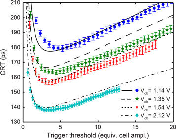
Figure 18. Comparison between predicted (lines) and measured (symbols) CRT of two 3 mm × 3 mm × 5 mm LYSO:Ce crystals coupled to Hamamatsu MPPC-S10362-33-50C SiPMs, as a function of the threshold voltage  and for different
  . © 2012 IEEE. Reprinted with permission, from Seifert et al (2012c).
Download figure:
Standard image High-resolution imageFigure 18 furthermore illustrates that  and
and  need to be jointly optimized. As the PDE and SPTR improve with increasing
  the best CRT is found at
  = 2.12 V in this experiment. Since the optimum threshold voltage is only a few times higher than the amplitude of the SSR, one would expect that the influence of the scintillator energy resolution (amplitude walk) is small, potentially favoring the use of simple, low-noise time-pickoff solutions, such as a LED, over more complicated circuits. Indeed, Seifert et al (2012c) found that the use of a CFD instead of a LED (both applied computationally to previously sampled waveforms) improved the measured CRT by less than 2%. Of course, in cases in which a suboptimal threshold and/or a very wide energy window is used, walk compensation may still be beneficial (Du et al
2017). Also, the dependence of the SiPM gain on temperature (see section 4.3.1) implies that the optimum threshold voltage my drift over time unless the SiPM gain is stabilized. This may be achieved, for example, by temperature regulation or automated adjustment of
= 2.12 V in this experiment. Since the optimum threshold voltage is only a few times higher than the amplitude of the SSR, one would expect that the influence of the scintillator energy resolution (amplitude walk) is small, potentially favoring the use of simple, low-noise time-pickoff solutions, such as a LED, over more complicated circuits. Indeed, Seifert et al (2012c) found that the use of a CFD instead of a LED (both applied computationally to previously sampled waveforms) improved the measured CRT by less than 2%. Of course, in cases in which a suboptimal threshold and/or a very wide energy window is used, walk compensation may still be beneficial (Du et al
2017). Also, the dependence of the SiPM gain on temperature (see section 4.3.1) implies that the optimum threshold voltage my drift over time unless the SiPM gain is stabilized. This may be achieved, for example, by temperature regulation or automated adjustment of  as a function of device temperature.
It was mentioned before that the influence on the CRT of crosstalk pulses generated by scintillation photons tends to be small. Crosstalk can nevertheless affect the time resolution of SiPM-based scintillation detectors in a different way, as shown by Gola et al (2014). Figure 19 shows the measured CRT of such a detector as a function of  at different temperatures. The curves can be explained in terms of the Seifert timing model.
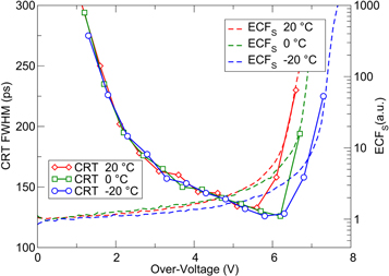
Figure 19. CRT versus  measured with 2 mm thick, Teflon-wrapped LYSO:Ce scintillators coupled to 2 mm × 2 mm FBK RGB SiPMs, at different temperatures, compared with the corresponding excess charge factor due to the scintillator (ECFS), i.e. the ratio of the measured dark current (dark counts plus crosstalk pulses generated by dark counts) with and without the scintillator on top of the SiPM. Reproduced from Gola et al (2014). © 2014 Institute of Physics and Engineering in Medicine. All rights reserved.
Download figure:
Standard image High-resolution imageThat is, up to about ∼2 V, the CRT is limited by the electronic noise term in equation (31) and the rapid improvement with increasing  is due to the increase of both the PDE (hence,
  ) and the SPAD gain (hence,
  ). It is noted that Gola et al (2014) eliminated the influence of dark count-induced baseline fluctuations using an analog filtering technique. Hence, only the (constant) noise of the readout electronics is included in the slope-over-noise ratio in this
  region.
Between about ∼3 and ∼6 V, readout noise is no longer dominant. In line with Seifert et al (2012c), we may assume that also the scintillator energy resolution and crosstalk contribute little to the CRT at these values of  In other words, we are now in the regime where equation (31) tends to reduce to equation (32). The CRT keeps decreasing since both the PDE (hence,
  ) and the SPTR (hence,
  ) improve with increasing
One would expect this trend to continue until the improvement of the PDE and SPTR saturates and/or the DCR becomes so large that adequate baseline restoration is no longer possible. The latter effect would give rise to an increase of the electronic noise term in equation (31). In fact, this term is expected to increase steeply above a certain value of  where the crosstalk probability reaches a value of 1 and the number of crosstalk pulses generated by dark counts starts to diverge. However, Gola et al (2014) stated that the PDE of their SiPM is not yet saturated at
  = 6 V, while crosstalk divergence is normally observed above ∼12 V only. This paradox was resolved when they found that the presence of the scintillator enhances the optical crosstalk probability. This external crosstalk component makes that divergence occurs more quickly, around ∼6 V in this particular measurement. Because of the temperature dependence of the (intrinsic) DCR, the exact value of
  at which divergence occurs is different for each curve in figure 19.
The increasing understanding of the factors that determine the time resolution of SiPM-based scintillation detectors has led to impressive results in benchtop experiments, which typically employ very small scintillation crystals to optimize  and
and  A CRT of ∼100 ps FWHM was achieved for the first time in 2009, using 3 mm × 3 mm × 5 mm LaBr3:Ce(5%) crystals coupled directly to 3 mm × 3 mm Hamamatsu S10362-33-050C SiPMs with 50 μm SPADs (Schaart et al
2010). The same value was reached a few years later by Schmall et al (2014) with 4 mm × 4 mm × 5 mm LaBr3:Ce(30%) crystals coupled to 4 mm × 4 mm NUV SiPMs from FBK with 50 μm SPADs. This group subsequently achieved a CRT as good as 69 ps FWHM with 4 mm × 4 mm × 5 mm CeBr3 crystals coupled to 4 mm × 4 mm FBK NUV-HD SiPMs, which had a better PDE than the NUV SiPMs used in the previous study (Schmall et al
2016).
A CRT of ∼100 ps FWHM was achieved for the first time in 2009, using 3 mm × 3 mm × 5 mm LaBr3:Ce(5%) crystals coupled directly to 3 mm × 3 mm Hamamatsu S10362-33-050C SiPMs with 50 μm SPADs (Schaart et al
2010). The same value was reached a few years later by Schmall et al (2014) with 4 mm × 4 mm × 5 mm LaBr3:Ce(30%) crystals coupled to 4 mm × 4 mm NUV SiPMs from FBK with 50 μm SPADs. This group subsequently achieved a CRT as good as 69 ps FWHM with 4 mm × 4 mm × 5 mm CeBr3 crystals coupled to 4 mm × 4 mm FBK NUV-HD SiPMs, which had a better PDE than the NUV SiPMs used in the previous study (Schmall et al
2016).
Around the same time, other groups were achieving sub-100 ps CRTs with LSO:Ce-like crystals, enabled by the ongoing development of SiPM technology as well as the optimization of the scintillation material (see section 3.2). For example, Nemallapudi et al (2015) coupled 2 mm × 2 mm × 3 mm LSO:Ce crystals co-doped with 0.4% Ca to 3 mm × 3 mm FBK NUV SiPMs with 40 μm SPADs and reached a CRT of 85 ps FWHM. This result was later improved to 73 ps FWHM using the FBK NUV-HD SiPM with 25 μm SPADs, which reaches a PDE as high as 55% near 420 nm (Gundacker et al 2016). In the meantime, Cates and Levin (2016) achieved 80 ps FWHM with 2.9 mm × 2.9 mm × 3 mm LGSO:Ce(0.025 mol%) crystals coupled to 4 mm × 4 mm FBK NUV-HD SiPMs with 25 μm SPADs, while Piemonte et al (2016) reported a CRT of ∼100 ps FHWM with 3 mm × 3 mm × 5 mm LYSO:Ce crystals coupled to the same type of SiPMs. In a more recent experiment, Gundacker et al (2019) coupled their 2 mm × 2 mm × 3 mm LSO:Ce,Ca(0.4%) crystals to 4 mm × 4 mm FBK NUV-HD SiPM with 40 μm SPADs (providing a higher fill factor than the 25 μm device) and no entrance window (enabling direct coupling of the crystal to the bare SiPM). The authors estimate that roughly ∼44% of the emitted scintillation light was detected in this setup. Using a readout circuit similar to that developed by Cates et al (2018) for SPTR measurements, they achieved an impressive CRT of ∼58 ps FWHM.
Such low CRT values are not yet achieved in SiPM-based whole-body TOF-PET systems, for which the current state-of-the art is in the range of 200–400 ps FWHM (Hsu et al
2017, Zhang et al
2018, Deng et al
2019, Rausch et al
2019, van Sluis et al
2019). In part, this difference is due to the use of much larger crystals, possibly in combination with light-sharing techniques, and the associated deteriorating effect of suboptimal  and
and  on the potential timing performance. The readout electronics challenges encountered in such multichannel systems are another factor of importance, therefore these will be briefly discussed in the next section.
4.3.5. Readout of SiPM-based scintillation detectors
In section 4.3.2 it was discussed that high-bandwidth readout electronics are required to preserve the rising edge and fast component of the SSR of a SiPM, see e.g. figure 12 (right). It was furthermore explained that the high sensor capacitance may result in unfavorable shaping of the SSR unless the preamplifier input impedance is kept small at signal frequencies (figure 15). Likewise, the initial slope of the SiPM signal in response to a scintillation pulse was found to improve strongly when the input impedance, including the series inductance of the wire connections, is kept to a minimum (figure 16).
An interesting way to mitigate these requirements is by equipping the SiPM with an additional terminal that is parallel-connected to all of the individual diodes through small capacitances (Dolinsky et al 2013, Yeom et al 2013, Jackson et al 2014). Such a 'fast' output can have an equivalent capacitance that is one or two orders of magnitude smaller than the anode–cathode capacitance. The gain is similarly reduced, but the SSR is significantly faster. Meanwhile, the anode–cathode pulse can be optimized independently for energy determination.
Another approach is bootstrapping, in which signal is passed from the cathode to the anode to balance the voltage across the device and reduce its effective capacitance. This can e.g. be done with a transformer, using one side of the transformer as a low-impedance current loop between the anode and the cathode. Excellent results can be obtained with balanced-to-unbalanced (balun) configurations (Cates et al 2018, Gundacker et al 2019) as well as balanced circuits (Zhang 2016).
Besides the transient response, baseline variation due to the long tails of dark counts can affect the CRT of a SiPM-based scintillation detector. Various solutions have been proposed. If the full waveform is sampled for each event, digital baseline restoration may be performed a posteriori (Schaart et al
2010, Gola et al
2012, Bieniosek et al
2016a). One may also consider high-pass filtering, e.g. by means of the previously discussed fast output (Yeom et al
2013, Jackson et al
2014) or an external CR filter (Dolinsky et al
2013, Bieniosek et al
2016a). However, the baseline may not be restored perfectly, as the application of a simple CR filter to exponentially decaying pulses tends to give rise to undershoot. This can be avoided by implementing a pole-zero (PZ) cancellation circuit rather than a CR filter in between the SiPM and the preamplifier (Knoll 2010). Indeed, Gola et al (2013) showed that a short pulse with a clean return to zero can be obtained if the PZ circuit is matched with 
Optimum implementation of such solutions in PET scanners with thousands of channels is less than trivial. Indeed, multichannel SiPM readout is a topic of much research. As it is impossible to discuss all developments in detail here, only some general trends are highlighted.
The possibility to digitize the waveforms of all detector pulses was mentioned already. Compact and affordable digitizers with sampling rates >1 GHz exist that facilitate multichannel implementation of this approach (Cho et al 2011, Ronzhin et al 2013, Ashmanskas et al 2014, Park et al 2018). Time-multiplexing can be used to reduce costs, but leads to an increased DCR on the multiplexed channel (Grant and Levin 2015, Kim et al 2016, Bieniosek et al 2016a, Won et al 2016a). At the time of writing, waveform sampling of individual events is mostly used in research setups.
Many TOF-PET systems use application-specific integrated circuits (ASICs) for reading out the SiPMs. A variety of ASICs has been developed in recent years, offering functionalities such as signal amplification, time pickoff, and energy determination, as well as secondary functions such as gain and offset regularization. Some ASICs are user-configurable, making them compatible with different types of SiPM and facilitating the development of prototype TOF-PET systems. Much effort is spent on the development of ASICs for SiPMs and the challenges are manifold; the classical tradeoff between bandwidth and power dissipation is just one of them. For details, the reader is referred to Calo et al (2019), who have recently reviewed the state-of-the-art in this field.
Digitization of the time information provided by an ASIC or other front-end circuit can be done using conventional TDCs. However, several groups have implemented TDC functionality in field-programmable gate arrays (FPGAs) (Fishburn et al 2013, Aguilar et al 2015, Won et al 2016b, Kim et al 2018, Venialgo et al 2019). This is considered an efficient approach as many PET systems already make use of FPGAs for processing the digitized data. Some groups even propose FPGA-only readout, feeding the SiPM signals directly into FPGA input/output (I/O) pins configured to act as voltage comparators (Xi et al 2013, Palka et al 2017, Won and Lee 2018).
4.3.6. Digital silicon photomultipliers (dSiPMs)
Similar to analog SiPMs, dSiPMs consist of a two-dimensional array of SPADs. Instead of a passive quench resistor, however, a logic circuit is integrated locally with each SPAD, as indicated in the simplified dSiPM microcell circuit shown in figure 20. The microcell electronics monitor the voltage across the SPAD and, when triggered by a discharge, execute an active quenching and recharge cycle. Moreover, each local circuit is connected to digital readout electronics elsewhere on the chip, such as a timing circuit and a photon counter (figure 21). Additional electronics may be integrated to control the operation of the sensor (including e.g. functionality for reducing the total DCR by masking noisy SPADs) and to acquire, (pre-) process, and read out the signals produced by the microcells. The state-of-the-art in dSiPM technology and its use in PET devices has recently been reviewed (Schaart et al 2016). Therefore, dSiPMs will be discussed only briefly and with a focus on timing performance.

Figure 20. Simplified circuit of the basic building block of a digital SiPM, the so-called microcell, which consists of a SPAD and the associated microcell electronics. Reprinted from Haemisch et al (2012). Copyright (2012), with permission from Elsevier. CC BY-NC-ND 3.0.
Download figure:
Standard image High-resolution image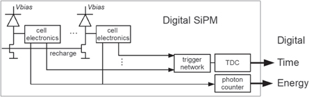
Figure 21. Schematic representation of a dSiPM. © 2009 IEEE. Reprinted, with permission, from Frach et al (2009).
Download figure:
Standard image High-resolution imageSimilar to analog SiPMs, the response of a dSiPM is non-proportional except under sparse illumination conditions. dSiPMs are not affected by after-pulsing, but saturation, crosstalk, and dark counts still play a role. The lower limit of the response of both analog and digital SiPMs is given by equation (20). Van Dam et al (2012b) developed a more comprehensive model of the expected value and variance of the number of photons counted by a dSiPM in response to a given amount of energy deposited in a scintillator.
The factors influencing the PDE of a SiPM were discussed in section 4.3.3. The fill factor is particularly relevant in the case of dSiPMs; the area taken up by the microcell electronics, TDCs, and auxiliary electronics can take up a significant fraction of the total sensor area. This is one of the reasons why so-called SPAD/TDC arrays, a device in which each SPAD is connected to its own TDC and that is used in e.g. 3D optical imaging (Veerappan et al 2011), are not commonly used in PET detectors. Since most of the time information is carried by the first few scintillation photons, see e.g. figure 4 (left), multiple SPADs can share the same TDC in dSiPM designs optimized for TOF-PET.
The SPTR of a single SPAD was discussed briefly in section 4.3.3. In a dSiPM, a locally integrated time pickoff circuit detects the breakdown of a SPAD (figure 20), preventing unfavorable pulse shaping as occurs in analog SiPMs (section 4.3.2). In principle, this allows the sensor designer to utilize the steep initial rise of the avalanche current (equation (21)) and apply a very low threshold level (Ghioni et al 2007). This makes the time pickoff process less sensitive to gain and shape differences between SPAD pulses, resulting in more accurate timing, better uniformity, and lower sensitivity to temperature drifts at the sensor level. On the other hand, new causes of time blurring come into play in dSiPMs. For example, the SPTR is affected by propagation time differences (skews) in the digital trigger network. Thus, careful balancing of the network is required (Haemisch et al 2012, Mandai and Charbon 2013). Other sources of timing uncertainty include the resolution and nonlinearity of the on-chip TDCs (which need to be optimized through calibration) and clock distribution jitter.
Besides the PDE and SPTR, the time resolution of a dSiPM-based scintillation detector is influenced by the rank(s) and the number of detected photon(s) used to estimate the time of interaction (figure 4). Whereas the threshold level of a time-pickoff circuit connected to an analog SiPM must be carefully optimized (figure 18), in a dSiPM this is the case for the logical operations applied to the timing signals produced by the microcells. In fact, the fully digital operation of dSiPMs make them true photon-counting devices, preserving at least partly the quantized nature of the time information embedded in the optical signal. As a result, the CRLB discussed in section 2.3 is well suited for the understanding and optimization of dSiPM design choices (e.g. the number of TDCs) and operational parameters (e.g. the trigger settings) (Seifert et al 2012b, Mandai et al 2014, Venialgo et al 2015).
Frach et al (2009) introduced the first dSiPM prototype developed specifically for PET. All SPADs in this device were connected to a single TDC via a balanced trigger network. Frach et al (2010) subsequently developed a production version of the device, known today as the Philips Digital Photon Counter (DPC). Each chip (also called die) comprises 2 × 2 pixels, each pixel containing 50 × 64 microcells. The four pixels share a pair of TDCs and an acquisition controller. A valid event in any of the pixels starts the acquisition in all four of them and the resulting digital data packet contains the photon counts and the timestamp of the trigger signal. Sixteen dies are combined into a 4 × 4 array (also called tile), thus providing 8 × 8 dSiPMs pixels in a 32 mm × 32 mm device (Degenhardt et al 2010). Using so-called neighbor logic, an event in one of the dies can be used to force data acquisition in one or more of its neighbors (Haemisch et al 2012).
The trigger network of the DPC can be programmed to timestamp either the first, second, third, or fourth registered photon of an event. Moreover, the device is equipped with so-called validation logic, to distinguish scintillation events from dark counts (figure 22). That is, once the trigger condition is met, a second, higher-level threshold must be passed within a user-defined validation time to complete the remainder of the acquisition cycle. Else, a fast reset is issued. Given that the duration of the readout cycle is in the order of hundreds of ns (limited fundamentally by the time required for integrating the scintillation pulse), such a provision is important to avoid excessive dead time, especially when the device is operated at low trigger settings and/or at high temperatures.

Figure 22. Schematic representation of the data acquisition cycle of the DPC3200 digital SiPM. Adapted from Tabacchini et al (2014). © 2014 IOP Publishing Ltd and Sissa Medialab srl. All rights reserved.
Download figure:
Standard image High-resolution imageThe trigger and validation conditions are implemented by subdividing the pixels into so-called sub-pixels and validation regions, respectively, and applying (configurable) logical interconnections to these sub-regions. Multiple cells may fire within a given sub-region, but only the first can change its logical state. Therefore, both the trigger and validation processes inherently are of a probabilistic nature and should be configured carefully to assure optimum operation of a dSiPM-based scintillation detector. To facilitate this analysis, Tabacchini et al (2014) derived an analytical model relating the probability of triggering and validation to the number of fired microcells.
The PDE of the DPC exceeds 40% at 420 nm (Kumar et al 2018). Brunner et al (2016) characterized the timing performance of individual SPADs, single pixels, and full DPC chips using a femtosecond laser. The SPTR of the SPADs was measured to be 48 ps FWHM, whereas the pixels and the entire sensor chip were found to be have SPTR values of ∼100 ps FWHM and ∼170 ps FWHM, respectively, when the 20% noisiest cells were switched off. The differences between these numbers were attributed to trigger network skews and electronic contributions. Van Dam et al (2013) measured a CRT of ∼120 ps FWHM using two DPC arrays operated in coincidence, each with a 3 mm × 3 mm × 5 mm LSO:Ce,0.2%Ca crystal coupled to one of its pixels. In similar setups, Yeom et al (2014) obtained a value of ∼135 ps FWHM with 3 mm × 3 mm × 5 mm LYSO:Ce crystals, Liu et al (2016) obtained a CRT of ∼130 ps FWHM using 2 mm × 2 mm × 5 mm LYSO:Ce crystals.
The DPC is the only dSiPM used in a commercial TOF-PET system at the time of writing. The sensor tiles are equipped with matrices of 4 mm × 4 mm × 19 mm LYSO:Ce crystals in a one-to-one coupling geometry and CRT values between 310 ps FWHM and 330 ps FWHM have been reported for this system (Zhang et al 2018, Rausch et al 2019).
Several other dSiPMs are under development for PET. For example, Braga et al (2014) presented the SPADnet-I sensor, a 9.9 mm × 5.5 mm device containing 8 × 16 pixels, each consisting of 4 so-called mini-SiPMs that share a data management circuit with photon counting and TDC functionality. The pixels are connected by an H-tree-like adder network that allows monitoring the total photon count at up to 100 Msamples/s, which is used for detecting and initiating the readout of scintillations events. As another example, the so-called multichannel digital SiPM can timestamp up to 48 photons per scintillation pulse while achieving a fill factor of ∼55% (Carimatto et al 2015, Venialgo et al 2015). This is made possible by making use of column-parallel TDCs.
Three-dimensional integration is an interesting approach to resolve the tradeoff between PDE and SPTR in dSiPMs. For example, a SPAD array fabricated in a custom process may occupy the top tier and a deep-submicron CMOS technology node can be used as the bottom tier. This allows connecting each SPAD to its own TDC without sacrificing fill factor (Tétrault et al 2015, Nolet et al 2016). In principle, one can calibrate the time response of each SPAD/TDC channel and compensate for skews occurring at the sensor level. Nolet et al (2018) designed and tested a 2D prototype of a single SPAD/TDC channel of such a device. They reported a SPTR of 17.5 ps FWHM for the complete channel (SPAD, quenching circuit, and TDC), which can be seen as a promising step towards the development of a full scale 3D digital SiPM. The same group recently presented an ASIC comprising a 16 × 16 array of SPAD readout circuits with in-pixel TDCs and embedded digital signal processing with an array timing jitter of ∼18 ps after skew correction (Nolet et al 2020).
5. New approaches in TOF-PET detector development
Chapters 3 and 4 summarize the state-of-the-art in scintillation materials and photon sensing technology, respectively. Innovations in both areas have made it possible to improve the CRT values of clinical PET scanners to ∼200 ps FWHM at the time of writing, while efforts towards ∼100 ps research systems are ongoing (Xie et al 2019). The introduction of the SiPM appears to be the main driver of time resolution improvement in clinical systems during the last ∼5 years. This is partly related to the fact that recent SiPMs offer PDE and SPTR values substantially better than those of PMTs (section 4.3.3). Another important factor is the improvement of the photon transfer kinetics resulting from the lower degree of light sharing (chapter 2); whereas the number of crystals in a PMT-based system typically is about two orders of magnitude larger than the number of sensor channels, this ratio is close to or equal to one in SiPM-based systems.
While further development of SiPM performance can be expected in the coming years, a very important parameter like the PDE already approaches ∼60% in some of the currently available devices. This, together with the fact that the efficiency and kinetics of optical transfer become more important as the CRT becomes smaller, necessitates new approaches to allow for substantial further progress. This chapter highlights some of the developments that could pave the way for sub-100 ps clinical TOF-PET systems, without losing sight of other crucial performance requirements.
5.1. Time-of-interaction estimators
Chapters 3 and 4 cover a series of developments that have enabled us to significantly increase the amount of time information available in PET detector signals. It is crucial to combine such hardware innovations with an efficient estimator of the time of interaction  for the CRT to approach the CRLB discussed in section 2.3. It was pointed out in sections 2.4 and 4.3.4 that relatively simple estimators, such as a LED, can approach the CRLB quite closely in a well-designed SiPM-based detector. Nevertheless, various studies indicate that the CRT can be improved in certain cases by using more advanced estimators.
For example, one may use a number of LEDs programmed at different threshold voltages to take multiple timestamps from an analog detector pulse and estimate  by linear interpolation or more advanced methods (Kim et al
2009, Deng and Xie 2015). Similarly, dSiPMs that have the capability of timestamping more than one photon per event allow improvement of the CRT using advanced estimators, not necessarily at great computational expense (Venialgo et al
2015, Lemaire et al
2020a, 2020b).
by linear interpolation or more advanced methods (Kim et al
2009, Deng and Xie 2015). Similarly, dSiPMs that have the capability of timestamping more than one photon per event allow improvement of the CRT using advanced estimators, not necessarily at great computational expense (Venialgo et al
2015, Lemaire et al
2020a, 2020b).
In setups in which the waveform of an analog detector is sampled, it has been shown that ML estimation can be performed efficiently on a subset of the full waveform and allows better time estimation than a digitally implemented LED especially if the sample rate is kept low to reduce costs (Barrett et al 2009, Ruiz-Gonzalez et al 2018). It has also been demonstrated that the TOF can be estimated directly from a pair of digitized detector waveforms by means of a convolutional neural network, using simple point-source measurements for obtaining the training data (Berg and Cherry 2018b).
5.2. Optimization of optical transfer
The importance of the optical transfer parameters  and
and  was discussed in chapter 2. Whereas the energy resolution is primarily affected by
  both
both  and
and  influence the CRT. That is, as many of the scintillation photons as possible must be transferred to the photosensor as quickly as possible.
Turtos et al (2016) stated that, even in well-designed scintillation light yield experiments, some 20% to 30% of the light remains trapped within the crystal. This suggests that one can enhance the CRT by improving the crystal-sensor coupling, also in existing PET detector designs. There are some obvious ways to achieve this, although they require careful implementation to be successful. For example, some scintillators are birefringent (van Dam et al
2012a), if only slightly so (Erdei et al
2012). Thus, the orientation of the crystal axes with respect to the photosensor can affect the light transfer in some cases. Potentially stronger effects may be expected from the geometric shape of the crystal, the treatment of the crystal surfaces, the choice of reflector material, and the way the reflector is applied. There are many publications on how these factors affect energy resolution, but these only address  and, therefore, cannot be extrapolated straightforwardly to timing performance. Understanding how the crystal geometry, surface treatment, and reflectors affect the CRT requires time-resolved simulations (Yang et al
2013, Ter Weele et al
2015c, Roncali et al
2017) and experiments (Gundacker et al
2014, Berg et al
2015, Ter Weele et al
2015b, Nemallapudi et al
2016b).
and, therefore, cannot be extrapolated straightforwardly to timing performance. Understanding how the crystal geometry, surface treatment, and reflectors affect the CRT requires time-resolved simulations (Yang et al
2013, Ter Weele et al
2015c, Roncali et al
2017) and experiments (Gundacker et al
2014, Berg et al
2015, Ter Weele et al
2015b, Nemallapudi et al
2016b).
Conventional approaches to minimize the probability of total internal reflection at the crystal-sensor interface include antireflective layers on the photosensor surface and the application of optical adhesives between the crystal and sensor. An approach currently under investigation is already used to enhance the light extraction from light-emitting diodes, viz the use of a thin slab of photonic crystal as a tunable, index-matching interface between the light emitter and the output medium. Salomoni et al (2018) have recently reviewed this research field. Promising results have been demonstrated and much of the current research is aimed at finding a reliable, scalable, and cost-effective production method for applying photonic crystal slabs on scintillators.
5.3. Novel detector designs
The methods discussed in sections 5.1 and 5.2 can be used to upgrade existing detector designs. A more fundamental step forward is to adapt the entire detector for optimum TOF-PET performance. This is an area where the possibilities of SiPMs are not yet fully exploited.
As mentioned in chapter 2, optical transfer kinetics become increasingly important at CRT values <100 ps FWHM. In essence, three causes of time resolution loss are associated with optical transfer: (1) the dependence of the mean optical path length between the point of interaction  and the photosensor on
  which in conventional, high-aspect-ratio crystals introduces a DOI-dependent signal delay; (2) the spread in the optical path lengths of the first detected photons for given
  which depends on the detector geometry and the properties of the optical interfaces; and (3) the dependence of this spread on
  Equation (18) offers a measure of the best achievable CRT in the presence of these three effects (Toussaint et al
2019). A simple way to reduce all of them in a conventional TOF-PET detector would be to reduce the crystal length, but this is at odds with the FOM defined in equation (2). Consequently, much of the current research focuses on the development of new detector geometries that minimize the optical transfer time dispersion and/or enable DOI-correction of the measured timestamps. The latter concept could be referred to as a form of time resolution recovery (TRR). Interestingly, the DOI can also be used to reduce parallax blurring in the reconstructed images (i.e. spatial resolution recovery).
Equation (18) offers a measure of the best achievable CRT in the presence of these three effects (Toussaint et al
2019). A simple way to reduce all of them in a conventional TOF-PET detector would be to reduce the crystal length, but this is at odds with the FOM defined in equation (2). Consequently, much of the current research focuses on the development of new detector geometries that minimize the optical transfer time dispersion and/or enable DOI-correction of the measured timestamps. The latter concept could be referred to as a form of time resolution recovery (TRR). Interestingly, the DOI can also be used to reduce parallax blurring in the reconstructed images (i.e. spatial resolution recovery).
Several TOF/DOI detector geometries are currently under study within this context. An obvious approach for high-aspect-ratio crystals (e.g. 3 mm × 3 mm × 20 mm) is dual-sided readout (DSR), in which photosensors are coupled to both of the 3 mm × 3 mm crystal faces. This reduces the OTTS and enables DOI correction at the same time. Simple time-of-interaction estimators, such as taking the average of the timestamps obtained on the front and back sides, appear to work quite well (Casella et al 2014, Seifert and Schaart 2015). The optical transfer characteristics influence the DOI and TOF performances in different ways, so a trade-off is typically made by fine-tuning the crystal surface properties or using a technique like sub-surface laser engraving (Blackberg et al 2018, Mohammadi et al 2019).
It is also possible to couple a one-dimensional array of SiPMs to one of the long (3 mm × 20 mm) sides of the crystal. Compared to DSR, the total photosensor area per crystal is even larger, resulting in excellent OTE and minimal transfer time spread. Indeed, outstanding CRT values have been demonstrated with this detector geometry (Moses et al 2010, Cates and Levin 2018).
Edge readout is a variation of the previous two themes, which literally approaches the positioning problem from a different angle. Here, rectangular scintillator slabs are stacked into a pile and sensor arrays are placed along the lateral edges of the slabs (Li et al 2018b, Peng et al 2019). The light distributions measured by the SiPM arrays are used to decode the interaction position, while the DOI is given by the slab number in which the event takes place.
Dual-sided, side, and edge readout all involve unconventional photosensor placement, where SiPMs have the important advantages of being compact and almost transparent to 511 keV gamma rays. There also exists a variety of TOF/DOI detector concepts based on more conventional backside readout (BSR). These can be broadly classified into methods based on pulse-shape modulation and light sharing.
In the well-known phoswich detector, each detector channel comprises two or more crystals with dissimilar pulse shapes (but, ideally, equal light yield), stacked on top of each other. The crystal layer in which the event took place is decoded by pulse shape analysis. Classification can be based on differences in decay time (Yamamoto et al 2016, Chang et al 2017, Ko and Lee 2017) or rise time (Schmall et al 2015). A variation on this concept uses a luminescent coating on the front part of a long crystal, which absorbs and re-emits a DOI-dependent fraction of the scintillation light, resulting in a modulation of the pulse shape (Kwon et al 2016a).
DOI encoding through light sharing can be achieved in various ways. A well-known approach is to stack two or more two-dimensional crystal arrays on top of each other, in such a way that the light emitted by crystals in different layers is distributed in different ways over the pixels of the photosensor array. Excessive light sharing deteriorates  so the light of each crystal should be shared among a few photosensor pixels only. Still, the light distribution should be unique for each crystal. Examples in which this has been achieved include an array of prism-shaped crystals stacked on a layer of rectangular crystals (Bieniosek et al
2016b) and multiple layers of rectangular crystal arrays that each have a different arrangement of reflector foils between the crystals (Yoshida et al
2015). DOI-dependent light sharing can also be achieved in a single-layer crystal array, e.g. using patterned reflectors between the crystals (Ito et al
2013, Lehnert et al
2016, Brown et al
2020), or by means of a light guide placed on the crystal array surface opposite to the photosensor (Niknejad et al
2017, Pizzichemi et al
2019).
so the light of each crystal should be shared among a few photosensor pixels only. Still, the light distribution should be unique for each crystal. Examples in which this has been achieved include an array of prism-shaped crystals stacked on a layer of rectangular crystals (Bieniosek et al
2016b) and multiple layers of rectangular crystal arrays that each have a different arrangement of reflector foils between the crystals (Yoshida et al
2015). DOI-dependent light sharing can also be achieved in a single-layer crystal array, e.g. using patterned reflectors between the crystals (Ito et al
2013, Lehnert et al
2016, Brown et al
2020), or by means of a light guide placed on the crystal array surface opposite to the photosensor (Niknejad et al
2017, Pizzichemi et al
2019).
It is emphasized that one cannot compare the CRTs reported in the above studies directly, as they were all obtained using different scintillation materials, sensors, electronics, and estimators. To judge how effective the different concepts are for the minimization of optical transfer time dispersion and/or DOI-correction of the timestamps, one should (1) compare the CRT to that obtained with a tiny crystal of the same material under otherwise equal experimental circumstances and (2) make sure that the CRT in both measurements is dominated by photon counting statistics, in other words that the contributions due to the readout electronics and the time estimation method are negligible.
While good CRTs have been reported for the designs mentioned in this section, they all have disadvantages. Pulse shape modulation and light sharing by definition are suboptimal from the viewpoint of photon emission and transfer kinetics. Pulse shape methods rely on a variation of the emission function  and/or the optical transfer time distribution
  with DOI, hence these functions cannot both be optimal at all depths. Light sharing tends to increase both the mean and the variance of the optical path lengths compared to one-to-one coupling. Strategies such as DSR and side readout do not have these issues; in fact, they do not affect
  tend to improve both
  and
and  and enable DOI-correction of the timestamps. Unfortunately, such unconventional sensor placement strategies are still often greeted with skepticism when it comes to the costs and practicality of implementing them in clinical systems.
5.4. Monolithic scintillator detectors
The monolithic scintillator detector is a TOF/DOI concept that, in its basic form, consists of a relatively large (typically several cm3), continuous slab of scintillation material read out by a pixelated photosensor coupled to the back surface. The three-dimensional position of interaction  in the crystal is derived from the measured light pattern, e.g. using a machine-learning algorithm. Thus, the essence of the concept lies in a combination of relatively simple hardware and advanced signal processing.
In fact, the simplicity of the hardware is at the root of the excellent TOF-PET performance that can be achieved with this type of detector. First, multiple timestamps are available per event, even if each photosensor pixel generates a single timestamp only. The lower bound on the CRT tends to decrease with an increasing number of time stamps, as illustrated by the blue circles in figure 4 (left). Second, the percentage of the total crystal surface covered by the photosensor is considerably larger than in a pixelated crystal array. This reduces the average number of reflections per photon and, therefore, the randomness in the optical transfer kinetics. Third, the timestamps recorded by the different photosensor pixels are strongly correlated with  So strongly, in fact, that they can be used as explanatory variables to estimate
  with decent accuracy (Tabacchini et al
2015). This correlation, combined with the fact that an estimate
with decent accuracy (Tabacchini et al
2015). This correlation, combined with the fact that an estimate  of
of  is derived a priori from the light intensity map, makes it possible to compensate for the influences of both the optical transfer time distribution
  and the SPTS
  of the photosensor. Van Dam et al (2013) demonstrated this using a ML algorithm that estimates the time of interaction
  from the measured set of timestamps, given
  on the basis of an empirical model of the order statistics that can be obtained from a simple measurement. In other words, they utilized the combined availability of
  and a set of timestamps to reduce the three causes of optical transfer time dispersion listed at the beginning of section 5.3, as well as the influence of the SPTR (all of which are taken into account in the derivation of equation (18)). Thus, the maximum-likelihood interaction-time estimation (MLITE) approach from Van Dam et al (2013) can be seen as an advanced form of TRR.
It is noted that the monolithic scintillator is not at all a new idea. Some of the earliest clinical PET systems were based on monolithic NaI(Tl) slabs read out by arrays of PMTs, even though these systems had no DOI capability yet (Karp et al 1990). The monolithic scintillator detector as we know it today was initially developed with preclinical and organ-specific systems in mind (Joung et al 2002, Bruyndonckx et al 2004, LeBlanc and Thompson 2004, Vaska et al 2004, Wilson et al 2004, Lerche et al 2005, Maas et al 2006, Llosà et al 2009, Schaart et al 2009, Kaul et al 2013, España et al 2014, Gonzalez et al 2016, Moliner et al 2017, Krishnamoorthy et al 2018, Gonzalez et al 2019). The use of such monolithic scintillators in clinical PET systems was in fact foreseen in an early stage already (Delorme et al 1996). However, the realization that monolithic scintillators are attractive for TOF-PET arose much more recently, as a result of the increasing insight into scintillation photon order statistics (section 2.3).
Using MLITE, Van Dam et al (2013) reached CRTs of ∼160 ps FWHM and ∼185 ps FWHM, respectively, with 10 mm and 20 mm thick monolithic LSO:Ce,Ca crystals coupled to dSiPM arrays in BSR geometry. This can be compared to the value of 120 ps FWHM achieved with 3 mm × 3 mm × 5 mm crystals of the same material on the same sensor. Around the same time, Seifert et al (2013) reached a CRT of ∼198 ps FWHM with a 10 mm thick LaBr3:Ce monolithic crystal coupled to an analog SiPM array. All of these measurements were done in BSR configuration.
A few years later, Borghi et al (2016a, 2016b) reached CRTs of ∼214 ps FWHM and 147 ps FWHM with 32 mm × 32 mm × 22 mm LYSO:Ce crystals in BSR and DSR configuration, respectively. These values may be compared to the value of ∼135 ps FWHM obtained by Yeom et al (2014) with 3 mm × 3 mm × 5 mm LYSO:Ce crystals coupled to the same type of dSiPM array. Moreover, Borghi et al (2016a, 2016b) reported detector spatial resolutions of ∼1.7 mm FWHM and ∼1.1 mm FWHM, in combination with DOI resolutions of 3.7 mm FWHM and 2.4 mm FWHM, for the BSR and DSR detectors, respectively. The energy resolution was ∼10% FWHM in all cases. Borghi et al (2015, 2016b) furthermore demonstrated a number of methods to make the calibration and operation of the monolithic scintillator detector in a full clinical PET system more practical.
Tabacchini et al (2017) simulated the expected imaging performance of the BSR and DSR detectors in comparison to pixelated crystal arrays with DOI capability. They concluded that a crystal pitch of 3.2 mm or 1.3 mm, in both cases with three DOI layers, would be needed to match the performance of the BSR or DSR detector, respectively, in terms of contrast recovery and small-lesion detectability.
Borghi et al (2018) subsequently demonstrated the imaging performance of the BSR detector experimentally in a 70 cm diameter tomographic setup. They measured a CRT of ∼212 ps FWHM in combination with an almost uniform spatial resolution of ∼3 mm FWHM, up to 25 cm radial distance if DOI correction was applied (figure 23).
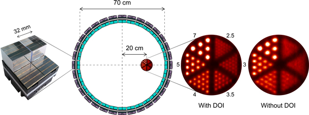
Figure 23. Left: photograph of a module with two out of four monolithic scintillator detectors mounted. Center: schematic overview of tomographic geometry. Right: TOF ML-EM reconstructed images of a Derenzo-like phantom with its center positioned at 20 cm radial distance, with and without DOI correction. The diameter of the hot rods is 2.5, 3.0, 3.5, 4.0, 5.0, and 7.0 mm. Adapted from Borghi et al (2018). © 2018 Institute of Physics and Engineering in Medicine. CC BY 3.0.
Download figure:
Standard image High-resolution imageAn increasing number of groups is performing research on monolithic scintillator TOF/DOI detectors, focusing, for example, on the further improvement of position estimation efficiency (Muller et al 2018), the use of analog SiPMs in such detectors (Lamprou et al 2020), and their application in clinical PET systems (Mikhaylova et al 2017, Vandenberghe 2018).
Figure 23 (right) illustrates a point of importance for the development of future clinical TOF-PET systems. PET reconstructed image resolution has long been limited by a lack of counts and the improvement of system resolution is clinically meaningful only if the SNR is improved as well (Phelps et al 1982). Due to the combination of TOF and longer axial FOVs, this is made possible today. Indeed, the high effective sensitivity of their systems has enabled some manufacturers to reduce the crystal pitch and improve the reconstructed resolution (Badawi et al 2019, van Sluis et al 2019). Consequently, parallax effects are expected to become more important (Kaul et al 2013, Thoen et al 2013) and it can be foreseen that future clinical TOF-PET systems will need detectors with DOI capability for both parallax correction and TRR.
Monolithic scintillator TOF/DOI detectors appear well suited for realizing these objectives in the near future. Remembering the FOM defined in equation (2), we see that the total photosensor area remains the same as in a system based on pixelated crystal arrays, while the crystal fill factor and, therefore, the term  reaches a maximum for a given crystal thickness. Combined with excellent timing, high spatial resolution, DOI capability, and good energy resolution, it appears reasonable to expect that monolithic scintillator detectors can enable the next milestone in clinical PET performance.
5.5. Prompt photons
Various researchers have investigated the use of radioluminescent processes other than scintillation for PET. For example, TOF-PET detectors based on the Cherenkov effect have been proposed (Ooba et al 2004, Miyata et al 2006, Dolenec et al 2010, Lecoq et al 2010, Brunner et al 2013, Somlai-Schweiger and Ziegler 2015, Ota et al 2019). Cherenkov photons are created almost instantaneously by the hot electron created upon the absorption of a 511 keV photon in a dielectric material, if the electron moves faster than the phase velocity of light in that material (Klein et al 2019). Other examples of processes that can lead to (near-)instantaneous ('prompt') emissions are core-valence luminescence (Shibuya et al 2010) and hot intraband luminescence (Omelkov et al 2018).
Important challenges in the application of such prompt emissions originate from the very low number of photons produced by a 511 keV photon (e.g. in the order of ∼101 in efficient Cherenkov radiators). This makes the CRT highly sensitive to the efficiency and kinetics of photon generation, transfer, and detection. Selecting only the events with the highest photon count typically yields the best CRT, but this goes at the expense of the term  in equation (2). Moreover, the low photon count complicates event positioning and energy determination.
To overcome these issues, Brunner and Schaart (2017) and Kwon et al (2016b) independently demonstrated the use of Cherenkov photons for timing in BGO, while relying on the scintillation light for energy and position determination. Figure 24 shows the luminescence response of BGO upon excitation by an annihilation photon, revealing a significant Cherenkov component with a FWHM of about 160 ps, preceding the slower (but much brighter) scintillation component.
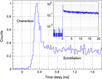
Figure 24. Luminescent response of BGO during the first 2 ns following excitation by 511 keV annihilation photons, measured using a dSiPM-based time-correlated single-photon counting setup. The inlay shows the response within the first 20 ns on a logarithmic time scale. Data taken from Brunner and Schaart (2017).
Download figure:
Standard image High-resolution image
BGO was used in many commercial PET systems until the 2000s, but manufacturers have mostly switched to L(Y)SO:Ce since then (chapter 3). BGO nevertheless ranks among the highest in terms of the parameters  ≈ 7.1 g cm−3 and
  ≈ 75 (cf. table 1), it is less expensive than lutetium-based scintillators, and has a high Cherenkov yield. Thus, the hybrid Cherenkov/scintillation approach may offer prospects for reviving BGO as a cost-efficient TOF-PET detector material, e.g. for use in emerging PET markets and/or total-body TOF-PET systems (Badawi et al
2019, Karp et al
2020). Again, the main challenge arises from the low Cherenkov photon count, which makes that the two timestamps of a given coincidence may arise from Cherenkov photons only, scintillation photons only, or a mixture thereof. This can result in non-Gaussian timing spectra, which needs to be taken into account during image reconstruction (Efthimiou et al
2020). Fortunately, more and more groups are picking up on the idea and better and better results are being achieved, amongst others through the use of the latest generation of SiPMs and readout electronics (Cates and Levin 2019, Gundacker et al
2019, Kwon et al
2019). Several variations on the hybrid readout theme have been proposed, such as Cherenkov/scintillation detection in liquid Xe (Ferrario 2018) or the combination of Cherenkov timing with energy and positon determination from charge collection in metalorganic liquids (Yvon et al
2014) and wide-bandgap semiconductors (Arino-Estrada et al
2019).
≈ 75 (cf. table 1), it is less expensive than lutetium-based scintillators, and has a high Cherenkov yield. Thus, the hybrid Cherenkov/scintillation approach may offer prospects for reviving BGO as a cost-efficient TOF-PET detector material, e.g. for use in emerging PET markets and/or total-body TOF-PET systems (Badawi et al
2019, Karp et al
2020). Again, the main challenge arises from the low Cherenkov photon count, which makes that the two timestamps of a given coincidence may arise from Cherenkov photons only, scintillation photons only, or a mixture thereof. This can result in non-Gaussian timing spectra, which needs to be taken into account during image reconstruction (Efthimiou et al
2020). Fortunately, more and more groups are picking up on the idea and better and better results are being achieved, amongst others through the use of the latest generation of SiPMs and readout electronics (Cates and Levin 2019, Gundacker et al
2019, Kwon et al
2019). Several variations on the hybrid readout theme have been proposed, such as Cherenkov/scintillation detection in liquid Xe (Ferrario 2018) or the combination of Cherenkov timing with energy and positon determination from charge collection in metalorganic liquids (Yvon et al
2014) and wide-bandgap semiconductors (Arino-Estrada et al
2019).
Whereas the timing theory of fast and bright scintillators is well understood (sections 2.3, 4.3.4), this is not the case for prompt photons yet. Gundacker et al (2016, 2018) and Lecoq (2017), Lecoq et al (2020) used the formalism by Seifert et al (2012b) to investigate the CRT improvement that could be achieved by adding a hypothetical, fixed number of prompt photons to the emission of existing scintillators. While this study provides qualitative insight into the influence of prompt photons on the CRT, the number of photons produced by the Cherenkov effect and other prompt phenomena is not at all fixed and, therefore, the quantitative results have to be considered with caution. Even more so, because the Seifert timing model itself may tend towards overly optimistic lower bounds for ultrafast and weak emissions (section 2.3). Given these uncertainties, Monte Carlo simulations may represent the most reliable method for time resolution calculations involving prompt emissions at the time of writing, provided that they are performed carefully and with attention for detail (Tetrault et al 2017, Kwon et al 2019). It is hoped that a useful lower bound of the CRT achievable with prompt emissions will be developed and validated in the near future.
5.6. Towards 10 ps PET?
The idea that direct three-dimensional measurement of the point of annihilation should be possible if gamma cameras had sufficient time resolution probably is about as old as the concept of coincidence detection itself. Combining the just-developed CRLB model of scintillator time resolution (Seifert et al 2012b) with knowledge of the fundamental performance limits of lanthanide-doped scintillators (Dorenbos 2010), Schaart et al (2011, 2012) predicted that the foreseeable development of SiPMs might at some point enable clinical PET systems with sub-100 ps FWHM time resolution. However, they also argued that (1) a CRT < 20 ps FWHM would be required to enable direct event localization in clinical PET, (2) such a paradigm shift would be hard to reach with lanthanide-doped scintillators, and (3) a new detector concept would therefore be needed to achieve this 'holy grail' of PET imaging.
These statements still appear valid at the time of writing (Schaart et al 2020b). In accordance with the calculations presented back then, Gundacker et al (2019) recently achieved CRTs of 58 ± 3 ps FWHM and 98 ± 3 ps FWHM with 2 mm × 2 mm × 3 mm and 2 mm × 2 mm × 20 mm LSO:Ce,Ca crystals, respectively. The crystals were coupled to high-end SiPMs, in a benchtop experiment in which all optical and electronic factors of importance were carefully optimized. While this achievement demonstrates excellent experimental skill, the SiPMs used had a PDE of ∼60% already, so it appears unlikely that a CRT improvement by a factor of ∼5 in realistically sized crystals will emerge from the further improvement of SiPM technology alone.
Interestingly, Ota et al (2019) recently achieved a CRT of 30 ± 2 ps FWHM using a pair of so-called Cherenkov-radiator-integrated MCP-PMTs. In essence, these are MCPs in which the entrance window has been replaced by 3.2 mm thick lead-glass Cherenkov radiator. As the photocathode is applied directly to the lead glass,  and
and  are greatly improved. Ota et al (2019) furthermore covered the lead glass top surfaces with black tape to avoid reflections and selected only the events with the highest photon count. They acknowledge that the resulting detection efficiency does not yet satisfy the requirements of a clinical PET detector (Ota et al
2020). Nevertheless, their outstanding experimental result shows that the physics of positron annihilation do not prohibit a CRT of 30 ps FWHM. This is an important finding that warrants continued research into ultrafast timing detectors.
are greatly improved. Ota et al (2019) furthermore covered the lead glass top surfaces with black tape to avoid reflections and selected only the events with the highest photon count. They acknowledge that the resulting detection efficiency does not yet satisfy the requirements of a clinical PET detector (Ota et al
2020). Nevertheless, their outstanding experimental result shows that the physics of positron annihilation do not prohibit a CRT of 30 ps FWHM. This is an important finding that warrants continued research into ultrafast timing detectors.
In fact, a variety of novel methods for timestamping annihilation photons with ultrahigh precision is currently under investigation. In particular, researchers in the high-energy physics community are advocating the '10 ps challenge' and the wide variety of radiation detection expertize available within this field is hoped to help enable a breakthrough at some point in future. Some of the novel approaches being proposed are based on ultrafast luminescent phenomena, such as Cherenkov radiation, cross-luminescence, hot-intraband luminescence, and tunable emissions from quantum-confined systems in nano- or metamaterials (Lecoq et al 2020). In addition to such self-generating transducer concepts, passive sensor approaches are being explored, for example based on the modulation of optical properties due to the interaction of ionizing radiation in transparent media (Lecoq et al 2014, Tao et al 2016).
Modulating sensors are beyond the scope of the theoretical framework that forms the basis of this review. Furthermore, it was explained that the results obtained by applying existing timing theory to the weak and (near-) instantaneous types of luminescence discussed in e.g. (Lecoq et al 2020) should be considered with caution (see the pertinent comments in sections 2.3 and 5.5). The more detailed discussion of novel timing approaches will therefore be left for future publication. At this point, it is hoped that more researchers will join this exciting new area of research and that they will not only hypothesize new methods for ultraprecise timing, but also contribute to the development of the theory needed to quantify and optimize their potential for TOF-PET. Moreover, it is hoped that they will work on new solutions with the clinical end in mind, taking into account, for example, the arguments that lead to equation (2).
6. Summary and conclusion
Since the introduction of the first commercial whole-body TOF-PET/CT scanner based on lutetium oxyorthosilicate crystals in 2006, a variety of TOF systems have been released. The benefits of TOF are well established; in fact, systems with TOF capability are considered the clinical standard in many countries today. State-of-the-art CRT values have improved from 500 to 700 ps FWHM in the second half of the 2000s to ∼200 ps FWHM at the time of writing. For a large part, this improvement has been made possible by the replacement of PMTs by SiPMs, which not only offer better PDE and SPTR, but also facilitate the optimization of the efficiency and the kinetics of scintillation light transfer.
This work discusses the factors that determine the time resolution of state-of-the-art PET detectors (figure 3). It discusses how the improvement of timing performance requires careful optimization of all pertinent aspects of the detection chain; one 'simply has to do everything right' to achieve the best possible CRT. A sound and quantitative understanding of the physics involved facilitates such efforts greatly. Therefore, this paper starts with a review of scintillation detector timing physics (chapter 2). It is shown how the quantized nature of the time information contained in the scintillation signal makes that order statistics dominate the time resolution of state-of-the-art detectors. As a result, CRLB analysis of the CRT appears a useful tool for the rational optimization of TOF-PET detector designs. It also offers an objective benchmark for analyzing the performance of hardware components as well as signal processing algorithms. Various groups have validated (and extended) this theory for the fast and bright scintillators used in current TOF-PET scanners. That said, its applicability to novel systems, e.g. based on prompt but weak emissions, needs to be examined in more depth.
Once the theoretical foundation has been set forth, chapters 3 and 4 discuss the main components of a TOF-PET detector: the scintillator and the photosensor. The parameters that influence timing performance are explained and the history and state-of-the-art in both areas are reviewed. It is shown how the optimization of scintillation materials, advances in photosensor technology, and the development of dedicated readout electronics all contribute to the ongoing improvement of CRT values. Maintaining the right balance between the relevant parameters is crucial. For example, a faster emission may not outweigh a reduction in light yield, while a better SPTR may not compensate for a loss of PDE.
Next, the importance of detector design is discussed (chapter 5). It is shown that the optimization of photon transfer kinetics becomes more and more important, the better the CRT becomes. Therefore, the development of detector designs that allow the minimization of optical transfer time dispersion and/or the recovery of the resulting time resolution loss should be a priority in the coming years. In general, a design that allows the independent measurement of the DOI facilitates TRR. An additional incentive for combining TOF and DOI capability is that PET system developers are starting to exploit the high effective sensitivity of TOF-PET systems to further improve the system spatial resolution, resulting in greater sensitivity to parallax errors (figure 23). The monolithic scintillator detector is one example of a design that enables the simultaneous optimization of time, energy, and spatial resolution, including parallax correction and TRR, while offering maximum detection efficiency as well as a practical format for implementation in clinical systems.
Given the current understanding of timing physics and the foreseeable developments in PET detector technology, a system-level CRT of about ∼100 ps FWHM, in combination with high detection efficiency, spatial resolution, and energy resolution, appears to be an ambitious but realistic target for the next generation of clinical PET systems. It will be interesting to see what will come next. In principle, neither the physics of positron annihilation nor the statistics of scintillation detector timing appear to rule out the possibility of improving the CRT below 100 ps, even though this will require the implementation of advanced methodologies such as TRR. Yet, it remains to be seen whether it will be possible to realize a system-level CRT in the order of ∼10 ps (Schaart et al 2020b). On the basis of the current knowledge, it appears unlikely that this can be achieved with detectors that utilize conventional scintillators (Schaart et al 2011, 2012). As a result, the search for new methods to timestamp annihilation photons with ultra-high precision is a rapidly growing area of research (Lecoq et al 2020).
Notwithstanding the exciting prospects, the aim to further improve time resolution must be put into perspective. For example, the experience obtained in the 1980s with TOF-PET systems based on BaF2 and CsF already teaches us important lessons about the trade-off between time resolution and other detector performance parameters (section 3.2). Throughout this review, the intent has been to not focus on time resolution per se, but to keep in mind that the goal is to improve the (quantitative) imaging performance of PET and to increase its value as a tool for research and (personalized) medicine.
The concept of total-body PET, for example, offers an alternative route towards greatly improved sensitivity and (therefore) reconstructed spatial resolution (Badawi et al 2019). It furthermore offers unprecedented clinical possibilities, such as sub-second total-body dynamic imaging (Zhang et al 2020). Even though total-body systems are still very expensive, there is little doubt that they will be successful as research tools. It will be exciting to see the outcomes of the studies performed with such systems and it cannot be excluded that these will significantly affect our insights into the clinical possibilities and potential of PET. This, in turn, may affect the current wisdom regarding trade-offs in PET scanner design. For example, total-body PET could push the emphasis in PET instrumentation R&D towards cost-effectiveness rather than just timing performance. In this context, it is interesting to compare the previously cited, two-meter long Explorer system at UC Davis with systems that have a reduced axial length but still reach ultrahigh sensitivity through excellent TOF performance, such as the PennPET Explorer (Karp et al 2020, Pantel et al 2020). More in general, highly sensitive but affordable systems could facilitate more widespread use of PET, e.g. by enabling new clinical applications.
In conclusion, at least three PET detector research priorities appear warranted for the coming years: (1) TOF/DOI detector concepts and TRR methods that enable the development of (sub-) 100 ps, high-resolution clinical PET systems for whole-body and/or organ-specific imaging, (2) cost-effective TOF-PET detectors to advance total-body PET and facilitate more widespread use of PET in general, and (3) novel approaches for timestamping annihilation photons with the aim to make 10-ps PET possible in future. It is hoped that this paper will be of help to researchers working on these as well as other TOF-PET instrumentation developments. There remain many exciting opportunities for physicists and technology developers to make meaningful contributions to the further development of PET and thereby increase the value of molecular imaging in clinical research and practice.
Acknowledgments
I would like to thank the many people in the field who have in one way or another helped me shape my thinking about medical imaging instrumentation, fast scintillation detectors in particular. Naturally, any single-author paper is biased to some degree. A particularly strong source of bias has been my collaboration with Herman van Dam and Stefan Seifert, with whom I have been fortunate enough to work together for about six years. During this time, we developed a way of thinking about scintillation detectors and timing that provides the perspective from which this review was written. It is hoped that this makes it a meaningful addition to other review and roadmap articles recently published on TOF-PET. I would also like to thank Francis Loignon-Houle and Maxime Toussaint for thoughtful feedback on my generalization of their RMSE large-crystal time resolution model. Finally, I would like to thank Fabio Acerbi, René Bakker, Giacomo Borghi, Stefan Brunner, Thomas Frach, Alberto Gola, Jan Huizenga, Ryosuke Ota, Torsten Solf, Andreas Thon, and Masao Yoshino for help with and input for some of the figures.