

Abstract
Infrared (IR) and terahertz plasmons in two-dimensional (2D) materials are commonly excited by metallic or dielectric grating couplers with deep-submicron features fabricated by e-beam lithography. Mass reproduction of such gratings at macroscopic scales is a labor-consuming and expensive technology. Here, we show that localized plasmons in graphene can be generated on macroscopic scales with couplers based on randomly oriented particle-like nanorods (NRs) in close proximity to graphene layer. We monitor the excitation of graphene plasmons indirectly by tracking the changes in reflection/absorption spectra of methylene blue (MB) or polymethyl methacrylate(PMMA) molecules deposited on the structure. Hybridization of spectrally broad graphene plasmon and narrow molecular oscillators results in enhanced oscillator strengths and Fano scattering related lines asymmetry in reflection spectra.
Export citation and abstract BibTeX RIS
1. Introduction
Plasmons in two-dimensional (2D) electron systems are characterized by deep-subwavelength confinement of electromagnetic energy enabling their applications in sensitive photodetection [1–4], electromagnetic emission [5], light modulation [6] and bio-sensing [7]. The wavelength of 2D plasmons defining their ultimate confinement is about two orders of magnitude below the free-space radiation wavelength. Strong localization of 2D plasmons is paid off by large momentum mismatch between plasmons and free-space photons. As a result, couplers with sub-micron feature size are required to excite 2D plasmons [7–10]. A typical size of grating elements is order of ∼300–100 nm in the far-infrared (IR) (1–30 THz) and ∼100–10 nm in the mid-IR (30–60 THz) spectral range [7, 10].
Mass reproduction of periodic sub-wavelength gratings using e-beam lithography is labor-consuming and expensive technology, especially when dealing with macroscopic (millimeter-scale) samples which are required for THz and IR detection and harmonics generation applications. However, if metal grating is strongly coupled to graphene, i.e. a thickness of separating spacer is well below the plasmon wavelength, the THz/midIR plasmon field is localized mostly under metallic elements [7, 11, 12]. In this regime, the dispersion of plasmons depends on the width of a metallic strip but not on gratings period [13, 14]. It is natural to question whether it is necessary to use a periodic grating for excitation of plasmons or periodicity plays a secondary role and the same effect can be achieved in aperiodic (random) structures? In this paper, we provide positive answer to the above question, and demonstrate that self-assembled arrays of randomly oriented nanorods (NRs) in close proximity to graphene can be exploited for excitation of THz/midIR plasmons.
Our approach to plasmon excitation using random structures is expected to contribute substantially to development of devices which exploit nonlinear harmonics generation in midIR/nearIR range [15, 16] and enhanced IR molecular oscillators [7, 10]. A nontrivial idea of using self-assembled nanoparticles may also significantly simplify the device fabrication and thus boost the development of new cheap graphene-based devices for midIR and subTHz/THz nanophotonics, photodetection, nonlinear optics, super-resolution imaging and many more. Indeed, macroscopic arrays of metallic nanoobjects are readily prepared by a number of cost-effective self-assembly methods including physical deposition, Langmuir-Blodgett, nanosphere lithography. All these methods provide an excellent alternative to expensive e-beam lithography.
However, a direct spectroscopic observation of graphene plasmons excited under the randomly oriented metallic nanoobjects faces serious experimental issues. Indeed, to extract a plasmonic contribution to absorption by using Fourier transform infrared spectroscopy (FTIR), one should obtain transmission/reflection spectra for both parallel and perpendicular polarized light in respect to gratings strips [13]. The oriented elements allow one use spectrum recorded in parallel polarization as a reference. In case of random NRs' orientation this symmetry is broken and a direct extraction of graphene plasmon band from a raw FTIR data is hampered.
In this letter, we report on indirect monitoring of localized graphene plasmon in the middle IR range of 1200–1600 cm-1 which is generated with help of randomly oriented particle-like Au NRs of ∼50 nm length and ∼13 nm in diameter which are strongly coupled to graphene. More specifically, we monitor the effects induced by graphene plasmon, namely the enhanced oscillator strengths of IR absorption transitions in methylene blue (MB) and PMMA molecules and Fano scattering processes caused by hybridization of broad graphene plasmon and narrow molecular oscillators. Note that term 'coupling' here does not mean the hybridization of graphenes and rods plasmons, which is hardly probable due to very different resonance frequencies. However, Au rods do compensate the mismatch of wave vectors for radiation in free space and inside graphene, thus, enabling the graphene plasmon excitation.
2. Methods
Multilayered graphene/Al2O3/Au rods structures shown in figure 1(a) were fabricated. Au NRs of ∼50 nm length and 9–14 nm in diameter were synthesized by seed-mediated protocol [17]. A quasi-homogeneous 1 cm2 macroscopic array of isolated Au NRs was deposited on SiO2/Si substrate by using polyvinylpiridine assisted method described elsewhere [18]. A typical image of deposited NRs is shown in figure 1(b) and the distribution of the rods diameter is shown in the inset. Lower resolutionscanning electron microscopy (SEM) image in figure S1(a) (available online at stacks.iop.org/NANO/32/035201/mmedia) of the supplementary data illustrates the homogeneous coverage of macroscopic area by NRs. The rods length distribution is presented in figure S1(b). Al2O3 spacers of 3–8 nm thick were deposited on top of rods by using atomic layer deposition method. The thicknesses of Al2O3 spacers were measured by using spectroscopic ellipsometry. Chemical vapor deposited monolayer graphene was transferred on top of the samples by using standard wet transfer technique (see supplementary for more details). Finally, a drop of 10–2 M of MB diluted in deionized water was deposited/dried on the sample surface with/without graphene or 300 nm thick PMMA film was deposited on the sample by spin coating technique.
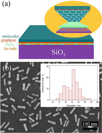
Figure 1. Multilayer graphene/Al2O3/Au-rods structure (a); a typical SEM image of Au nanorods on SiO2/Si substrate (b); distribution of Au rods' width is shown in the inset.
Download figure:
Standard image High-resolution imageThe following samples were prepared: bare Au 50 nm rods/SiO2 (Sample A), Au 50 nm rods capped by 4 nm of Al2O3 (Sample B), Au 50 nm rods with Gr deposited on top (Sample C) and Gr/Al2O3/Au rods structures (Sample D, E and F) with 4 nm, 6 nm and 8 nm Al2O3 spacers, correspondingly. Besides, similar samples containing 100 nm or 180 nm Au NRs were also studied (see supplementary).
3. Results
A typical Raman spectrum of reference sample with graphene on SiO2/Si substrate is shown in figure 2(a). It reveals a high frequency E2g Raman active phonon (G peak) at ∼1596 cm-1, A1g mode (D peak) at ∼1333 cm-1 and 2D mode at ∼2651 cm-1 which corresponds to two-photon scattering process. Note, that D mode represents a breathing of six-atom ring and is activated when point defects are present [19].

Figure 2. Raman scattering spectra of graphene/SiO2/Si (Sample A) (a) and graphene/Al2O3/Au-rods/SiO2 (Sample D) (d); the statistics of G and 2D modes' width is shown in corresponding histograms (b), (c) for Sample A and (e), (f) for Sample D. A strong fluorescent background in spectrum (d) is subtracted.
Download figure:
Standard image High-resolution imageA typical Raman spectrum for samples with graphene deposited on Au NRs/SiO2 substrate is shown in figure 2(d). All G, D and 2D modes for samples with NRs are shifted to red compared to similar phonons in graphene deposited on smooth SiO2/Si surface and are observed at 1586 cm-1, 1318 cm-1 and 2634 cm-1. The significant shift of all G, D and 2D modes to smaller photon energy is likely related to strong tensile strain in graphene induced by large roughness of the surface with Au NRs. A shift of 2D mode was reported by Zhang et al for graphene deposited on top of Ag particles [20]. Similar shifts and broadening of all graphene modes were also reported for graphene suspended on pair of Au nanodisks [21]. A tensile strain is opposite to previously discussed effect of compressive stress in graphene capped by SiO2 layer upon annealing where G, D and 2D modes are shifted to larger photon energy for ∼15 cm-1, 13 cm-1 and 29 cm-1, correspondingly [22]. A statistics of graphene spectra is analyzed by measuring Raman signal map at 25 points on the samples surface and is shown in histograms figures 2(b), (c) and (e), (f) and for graphene on flat and rough surface with NRs correspondingly. See also Table TS1 for more details.
Both ID/IG ratio, the width of D peak as well as G peak are increased in case of Gr/Al2O3/Au-rods samples which evidences that a larger amount of zero-dimensional point-like defects are activated compared to graphene on smooth SiO2/Si surface [23, 24]. More specifically, the widths of D, G and 2D modes are 40 ± 16 cm-1, 38 ± 7 cm-1 and 46 ± 3 cm-1 in Gr/Al2O3/Au-rods samples which are larger than 34 ± 5 cm-1, 11 ± 2 cm-1 and 37 ± 2 cm-1 measured for Gr/SiO2/Si structures. It is known that not all defects can contribute to increased ID/IG ratio but only those do which activate electron scattering between K and K' valleys [25].
Optical transmission spectra of Gr/Al2O3/Au rods structure (Sample D) and bare Au NRs/SiO2 (Sample A) as well as of Sample B with Au rods capped by Al2O3 layer and of Sample C with graphene deposited directly on rods are shown in figure 3(a). Here we discuss only the samples with 50 nm Au rods. The other spectra of samples with 100 nm and 180 nm Au rods which reveal similar trends are available in supplementary.
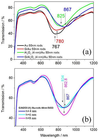
Figure 3. Optical transmission spectra of bare Au 50 nm rods (Sample A) (black), rods with graphene layer on top (Sample C) (red), rods with deposited 4.4 nm Al2O3 film only (Sample B) (green) and Gr/Al2O3(4 nm)/Au rods/SiO2 nanostructure (Sample D) (blue) (a); altered transmission of Gr/Al2O3(h)/Au rods/SiO2 structures in Samples D, E and F with altered spacer thickness h (b).
Download figure:
Standard image High-resolution imageOptical absorption spectra allow one to follow the details of rods-to-graphene coupling. Spectra of bare Au rods in Sample A reveal a major band of longitudinal plasmonic mode with maximum at 767 nm and minor band at 516 nm, corresponding to transversal plasmon. A major plasmon band describes a result of superposition of resonances in many individual rods. Therefore the width and position of the band are influenced by positions and damping factors γ of individual plasmons as well as by rods size distribution. Upon the depositing of Al2O3 layer on rods the dielectric constants of a surrounding particle medium are altered which results in a red shift of the rods' plasmons. More specifically, a longitudinal plasmon band at 767 nm observed in Sample A is red shifted for ∼58 nm upon the depositing of 4 nm Al2O3 layer as shown in figure 3(a). Similar shifts of longitudinal plasmons in samples with 100 nm and 180 nm Au rods are shown in figures S4 and S6. The details of on positions and widths of discussed plasmons are summarized in table TS2.
Deposition of graphene on top of Al2O3/Au rods results in further red shift of rods plasmon as shown in figure 3(b) and table TS2. More specifically, a longitudinal plasmon of 50 nm Au rods is shifted for 100 nm, 71 nm and 96 nm in respect to resonance of bare Au rods at 767 nm upon the rods are capped by corresponding 4 nm, 6 nm and 8 nm Al2O3 layers. Similar shifts for 100 nm and 180 nm rods are shown in figures S5 and S6. Deposition of graphene immediately on top of Au NRs results also in minor red shift of longitudinal plasmon. In particular, in case of 50 nm rods the plasmon band is red shifted for 13 nm which accords well to 10 nm shift observed for Ag particles coupled to graphene reported by Zhang et al [20]. In both cases when rods are touching graphene as well as when they are electrically isolated the plasmon band is broadened, which also is in agreement with previous studies [20, 26, 27] and is understood in term of increased Ohmic losses (and also damping rate γ) induced by penetration of plasmonic field into graphene. In addition, for rods which do contact graphene the plasmon is suppressed as shown in figure 3(a) which supports the assumption on decreased plasmons' Q-factors. Remarkable, that for samples with graphene isolated from Au rods with dielectric spacer a plasmon intensity is much less affected by nearby graphene layer, however the band is broadened as shown in figures 3(a) and S4, S6. We speculate that additional red shifted plasmonic mods are likely generated in result of strong coupling which are similar to those observed for particles coupled to continuous metallic film [28]. In particular, Okamoto et al found that these additional modes become more pronounced with increase of the Ez component of incident radiation which is perpendicular to the substrate. We speculate that in system of coordinate of an NR an appearance of Ez component is activated by (i) curved surface of graphene laying on a rough surface. Besides, a strong coupling likely also results in increased light scattering which broadens low energy part of transmission spectra. A careful analysis of plasmon band width for Samples D, E and F shown in figure 3(b) reveals a slightly decreased extinction for sample F with thicker Al2O3 spacer (see table TS2). Indeed, new types of plasmonic oscillations should become less pronounced at larger rod-to-graphene gap as the 'tails' of the enhanced electric field near Au rods worth penetrate to conducting graphene layer in that case. Similar effect was found for samples with 100 nm rods as shown in figure S5. More details on reduction of the width of rods' plasmons with decrease of 'coupling strength' can be found in table TS2. In particular the width of longitudinal plasmon band (measured at I0/ ) is reduced from 209 nm to 185 nm for samples with 50 nm rods and from 250 nm to 218 nm for samples with 100 nm rods when spacer thickness is increased from 4 nm to 8 nm.
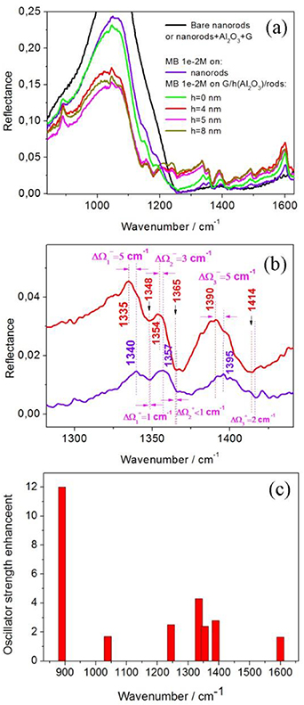
We use organic molecules as reporters to monitor the excitation of graphene plasmon in the middle IR range assisted by randomly oriented particle-like NRs which are strongly coupled to graphene. Bruker Vertex 80 V FTIR spectrometer equipped with Hyperion 2000 microscope and liquid nitrogen cooled MCT detector shown in figure S7 was used to record IR reflection/transmission spectra. MB and PMMA molecules have many narrow molecular oscillators in the range of 800–1600 cm-1 [29]. All the samples with bare Au rods or Gr/Al2O3/Au rods without MB layer on top do show nearly identical reflectance spectra with characteristic broad band at ∼900–1250 cm-1 assigned to SiO2 phonon absorption as shown in figure 4(a). Zoomed spectrum is shown in figures 4(b) and S8. Upon the deposition of dye molecules a number of spectral features are appeared which describe the absorption by molecular oscillators [29]. Comparison of reflectance/absorbance spectra measured on the surface of the very same sample in area with and without graphene reveal that MB molecules deposited on Gr/Al2O3/rods/SiO2 show larger molecular oscillator strengths compared to those observed for MB/rods/SiO2 sample as shown in figure 4(a). Besides spectral features in reflection spectra are shifted in samples with graphene as shown in figure 4(b). Interesting that oscillator strengths are better enhanced in Samples D-F with Gr/Al2O3/rods/SiO2 structures compared to Sample C where graphene has electric contact with metallic rods. The estimated enhancements of molecular oscillator strength induced by generated graphene plasmon are shown in figure 4(с). By analyzing these enhancements of many close positioned molecular oscillators one may visualize a position of generated broader graphene plasmons which induce the observed effect. Moreover, the present enhancement itself evidences the fact that graphene plasmon is indeed generated with assistance of randomly oriented Au NRs. Interesting, that apart from graphene plasmon band at ∼1000–1600 cm-1, even greater enhancement is also detected for molecular oscillator at 890 cm-1. We speculate that a rod is able to generate graphene plasmons which are collinear or perpendicular to the rods main axis. Indeed, the rods of ∼50 nm length and ∼13 nm diameter do likely excite two corresponding plasmons at ∼1300 cm-1 and ∼900 cm-1 which agrees well with theoretically estimated dispersion for graphene plasmons which are strongly coupled to strips of periodic metallic grating [13, 30–33]. The details on enhanced MB oscillators and spectral features shifts are available in Table TS3. As shown in Figure S9 a similar increased strengths of narrow PMMA molecular oscillators are observed in transmission/reflection spectra of PMMA(300 nm)/Gr/Au rods/SiO2 sample in the range of 1100–1740 cm-1, which supports our statement on generation of graphene plasmon associated to rods of 13 nm in diameter. A lowered transmission is also observed in the range of ∼600–1000 cm-1. Unfortunately, the oscillators of PMMA which are excited in this range are broad, which does not provide enough confidence that graphene plasmon which corresponds to the 50 nm length of NRs is generated in this sample.
Figure 4. Middle IR reflection spectra of MB molecules (10–2 M) on graphene/Al2O3/50 nm Au rods/SiO2 substrates with altered thickness h of Al2O3 spacer. Spectra of bare Au rods (Sample A) and graphene/Al2O3/Au rods/SiO2 structures (Samples D,E,F) without MB molecules are nearly identical (black) (a); zoomed spectra of Samples D with deposited MB taken in areas with/without graphene to illustrate SEIRA induced spectral shifts and enhanced oscillator strengths (b); graphene plasmon induced enhancement of strengths of MB molecular oscillators (с).
Download figure:
Standard image High-resolution image
4. Discussion
Reflection spectra of all the samples with graphene and deposited molecules also reveal spectral shifts up to 5 cm-1 and asymmetric shape of lines related to molecular oscillators in the range of 1200–1650 cm-1 which is typical for so called Fano scattering processes due to coupling of broad graphene plasmon with narrow MB or PMMA oscillators [34, 35]. Notable that molecular oscillators are affected only in the range where graphene plasmon is expected. Indeed, earlier reports [13, 30–33] showed that periodic metallic grating with strips of 9–14 nm width which are strongly coupled to graphene should assist excitation of spectrally broad localized graphene plasmon in the range of ∼1200–1600 cm-1, which accords well with our results. Similar effects induced by coupling of broad and narrow resonances which result in Fano scattering are also observed in other studies for metallic gratings [33] and meta-surfaces [35] coupled to graphene and molecules, graphene nanoribbons coupled to molecules [7, 10], periodic terahertz dipole nanoantennas spaced by nanogaps and coupled to quantum dots [36], and other coupled plasmonic systems [34, 37, 38].
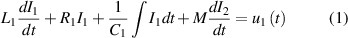
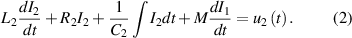
An analogy of Fano resonance to classical harmonic oscillator system was discussed in several studies [34, 37, 38]. Indeed, a coupled broad graphene plasmon at ω1 and narrow molecular oscillator at ω2 with damping rates of γ1, γ2 (γ1 ≫γ2) are described by pair of Kirchhoff's equations similar to those describing the current oscillations in a pair of inductively coupled electric RLC-circuits, on which two harmonic electromotive forces u1(t) and u2(t) do effect:
By introducing a dimensionless coupling constant  , normaized electromotive forces
  ,
,  , damping rates
  ,
,  and eigen-frequencies of decoupled circuits
  ,
,  , we find the ampltudes of current oscilations in coupled system (see supplementary for more details):
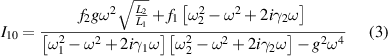
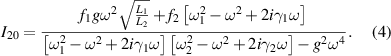
Current amplitudes  and
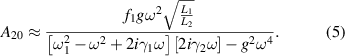
and  in this two RLC-circuits are mathematically described exactly the same as amplitudes of electronic oscillations in graphene plasmon and molecular dipole oscillator, correspondingly. At frequency ω ≈ ω2
of molecular oscillator one may assume that
in this two RLC-circuits are mathematically described exactly the same as amplitudes of electronic oscillations in graphene plasmon and molecular dipole oscillator, correspondingly. At frequency ω ≈ ω2
of molecular oscillator one may assume that  , i.e. only a graphene plasmon is coupled to external field and molecular dipole oscillations affected by plasmon follow the equation similar to
A coupling constant is responsible for repulsion spectral features near frequencies of molecular oscillators and the dispersion of refractive index, and, thus, a reflection spectrum of a graphene-molecule hybrid is altered. Therefore, narrow molecular oscillators as well as broad graphene plasmon do reveal extra shape asymmetry. Moreover, when molecular oscillator is coupled to graphene plasmon near molecular resonance the dispersion is altered with different rate. In result a lower energy part of reflection spectrum near molecular resonance, i.e. a 'peak' part is faster shifted to lower energy compared to higher energy 'valley' part. This effect is well resolved in observed reflection spectra in figure 4(b) where spectral shifts of 'peaks' ΔΩ- as large as 5 cm-1 and some smaller alterations of 'valleys' ΔΩ+ are detected. Moreover, the greater spectral shifts are observed for lines with greater enhanced oscillator strength, which well agrees to the model. See also table TS3 for more details on some resolved shifts ΔΩ- of peak feature of lines in reflection spectra.
Graphene-based structures are extensively studied for their possible applications in optoelectronic devices with electrical tuning of mid-IR plasmons [39]. By now our efforts to homogeneously deposit chemically functionalized Au rods on top of Al2O3/graphene surface faced to serious experimental issues. However, we believe that above difficulties will be overcome in further studies. During the publication of this research we became aware that Epstein et al have recently succeed in depositing the Ag nanocubes on hBN/graphene structure and demonstrated the electrical tuning of graphene plasmons [40]. Moreover, the spectral range of graphene plasmons excited with help of 50 nm nanocubes well corresponds to our results for Au rods-graphene hybrids. Thus, we believe that our results will find applications in future gate tunable graphene-based IR photonic devices.
Strong nonlinear optical response of graphene is extensively studied in broad spectral range from the near-IR [41] to THz [15]. Obtained generation of high harmonics [16] and combined frequencies by applying four-wave mixing schemes [15] enables one to design new types of ultrafast photonic devices [16, 42]. We believe that our approach of using hybrid graphene-nanoparticle systems to excite THz/middle IR plasmons will contribute substantially to development of this topic.
In summary, the organic molecule are used as reporters to indirectly monitor the generation of graphene plasmons assisted by aperiodic self-assembled arrays of metallic NRs. The strengths of molecular oscillators are 4–12 times enhanced by localized electric field near graphene surface within broad plasmonic bands. Hybridization of broad graphene plasmon and narrow molecular oscillators results in Fano scattering related asymmetry of reflection spectra. The proposed idea of using nanoparticles to excite graphene plasmons may boost the development of new cost effective graphene-based devices for middle IR and subTHz/THz nanophotonics, graphene harmonics generation, super-resolution imaging and photodetection.
Acknowledgments
Sample fabrication, study of middle IR properties, Raman scattering and modeling were supported by Russian Science Foundation, Grant No. 16-19-10557. Samples were fabricated using equipment of MIPT Shared Facilities Center with financial support from the Ministry of Science and Higher Education of the Russian Federation, Grant No. RFMEFI59417X0014. Atomic layer deposition was supported by Research Program No. 066-2019-0004 of the Ministry of Science and Higher Education of the Russian Federation. Study of optical absorption properties was supported by Russian Foundation for Basic Research according to the research project No. 18-02-00151A.
Supplementary Material
Supplementary material for this article is available online