
Abstract
A graphene/In2O3 bilayer (termed as GI-bilayer) is proposed as a transparent conducting electrode with remarkably improved areal-uniformity. To fabricate this new structure, an In2O3 layer with a thickness of less than 50 nm was grown by atomic layer deposition and then a graphene layer was grown by chemical vapor deposition and subsequently transferred onto the as-grown In2O3 layer. Electrical and optical properties of the GI-bilayer were systematically studied to verify effects of the underlying In2O3 layer. Hall measurements and following analysis showed a conductance enhancement of the GI-bilayer owing to p-type doping of graphene. Specifically, Raman analysis and ultraviolet photoelectron spectroscopy were performed to prove p-type doping of the graphene in the GI-bilayer. In addition, the GI-bilayer exhibited the significantly improved uniformity of the sheet resistance compared to that of a conventional monolayer of graphene. There was a duality on the role of the In2O3 underlayer in the GI-bilayer. It acted as a dopant layer to the graphene and lowered the sheet resistance from 863 to 510 Ω/sq as well as compensated microscale defects on graphene. More importantly, the In2O3 underlayer resulted in the extremely reduced standard deviation of sheet resistance from 150 to 7.5 Ω/sq over the area of 49 cm2.
Export citation and abstract BibTeX RIS

Original content from this work may be used under the terms of the Creative Commons Attribution 3.0 licence. Any further distribution of this work must maintain attribution to the author(s) and the title of the work, journal citation and DOI.
1. Introduction
Transparent conducting electrode (TCE) is one of the most important components of various optoelectronic devices such as touch screen panels [1], displays [2], solar cells [3], and light-emitting diodes [4]. In such applications, a sheet resistance less than 100 Ω/sq with a high optical transmittance to visible light (above 90%) is typically required to satisfy the minimum industrial standard established for TCE materials [5]. Currently, Sn-doped indium oxide—known as indium tin oxide (ITO)—is widely used as a TCE material because of its low resistivity (∼10–4 Ω cm) as well as its high optical transmittance at visible wavelengths [6]. However, TCEs based on oxide materials have a limited application in flexible electronics owing to their inherent brittle nature originated from either ionic or covalent bonding in plastic deformation [7, 8]. In this context, graphene has been proposed as an attractive TCE material for flexible optoelectronic devices [9–11]. As is well known, graphene comprises a single layer of carbon atoms having in-plane sp2-bonds and shows a unique combination of electrical, optical, and mechanical properties that are suitable for flexible TCEs [12–15]. In that sense, graphene has been considered as reinforcement to improve the mechanical flexibility of brittle oxides [16–20]. One such example is constructing a bilayer structure consisting of graphene and oxide film. For instance, Liu et al fabricated graphene/ITO bilayer structure and conducted electromechanical tensile and bending tests [17]. They showed that the change on electrical resistance of graphene/ITO bilayer was effectively retarded in contrast to bare ITO films, whose resistance increased rapidly as the strain increased. Lee et al also showed enhanced electromechanical durability of ITO/graphene bilayer in comparison with polycrystalline ITO films [19]. In these cases, graphene in bilayer structure acted as mechanical support for protecting a failure of brittle ITO [17–20]. Theoretical analysis based on fracture mechanics revealed that incorporated graphene layer enhanced fracture energy of oxide film in bilayer structure [18, 20]. These results clearly demonstrated that fracture resistance of graphene/oxide bilayer structure could be remarkably enhanced compared to that of brittle oxide.
As well as the advantages of the hybridization on mechanical properties, there have been several attempts to investigate the electrical properties of graphene/oxide bilayer structure [21–27]. In spite of significant progress for growth, transfer, and doping of graphene [28–32], several limitations still exist for practical applications of graphene-based electrodes: electrical conductivity of single-layer graphene is still too lower than that of conventional ITO, and a lack of large-area electrical reliability of graphene electrode [13, 33]. In particular, both macro- and microscale defects that can be generated during the growth and transfer process are known to critically deteriorate the large-area electrical reliability of graphene electrode [34, 35]. Several methods including usage of heptane as a transfer medium with improved contact between graphene and target substrate have been proposed to minimize microscale defects in graphene [33–36]. However, these approaches are still far from industrial applications due to the number of target substrates they can be applied to being limited [34] or the additional requirement for a suspending holder [36]. To overcome these shortcomings of the electrical properties of graphene via hybridization with oxide, considerable efforts have been devoted [21–27]. On depositing a few nm of MoO3, V2O5, WO3, and ZnO on graphene, metal oxide induced charge transfer doping of graphene was attributed to the work function difference of two materials [22–24, 26]. In addition, Lee et al demonstrated flexible organic light emitting diodes which exhibited superior external quantum efficiency of 40.8% for single-junction structure owing to the synergetic interplay of graphene/TiO2 bilayer electrode [16]. In that sense, graphene/oxide hybridization could provide a strategy for the realization of graphene-based electrodes in optoelectronic devices.
To this end, we propose a bilayer structure comprising graphene and In2O3, focusing on large-area electrical uniformity and analysis on its transport properties. This new structure is termed as GI-bilayer. The GI-bilayer was prepared by transferring CVD-grown monolayer graphene onto atomic layer deposition (ALD)-grown In2O3. As shown in figure 1, homogeneously deposited conducting In2O3 layer was introduced as a complementary layer to provide an electrical path to circumvent the microscale defects on the graphene and enhance the electrical property of graphene. We report the effects of a complementary In2O3 layer on the areal-uniformity of the sheet resistance, electrical properties, and optical transparency in terms of the thickness of the In2O3 layer. In addition, we also conducted a detailed analysis of the change in electrical properties of graphene and In2O3 sublayers induced by hybridization. It provides insight into the effects of the hybridization on electrical properties of the p–n-layer-stacked bilayer. (i.e. p-type of graphene and n-type of In2O3) As a result, we could obtain large-area uniformity of the conductance using the In2O3 underlayer only with a few nanometers thick despite the presence of microscale defects on the graphene. Moreover, the GI-bilayer exhibited remarkably enhanced electrical conductance owing to p-type doping on the graphene. Hall measurements and following analysis with multilayer Hall measurement model [37], Raman spectrum, and ultraviolet photoelectron spectroscopy (UPS) are used to further investigate the nature of p-type doping on the graphene in GI-bilayer.
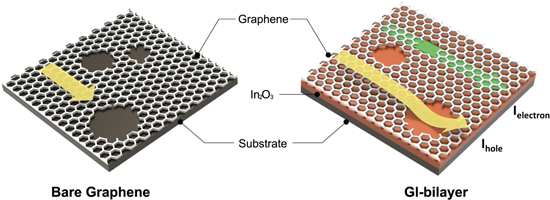
Figure 1. Schematic diagram of GI-bilayer. The GI-bilayer was prepared by transferring CVD-grown monolayer graphene onto ALD-grown In2O3. Underlying In2O3 layer in GI-bilayer provides an electrical bypath to circumvent the microscale defects on the graphene.
Download figure:
Standard image High-resolution image2. Experimental details
2.1. Deposition of In2O3 film
In2O3 thin films were deposited using an flow-reactor type ALD system (LUCIDA D-100, NCD Co., Ltd, Korea) at a deposition temperature of 217 °C as reported in our previous results [38]. Trimethylindium (TMIn, EG Chem Co., Ltd, Korea) and water vapor (H2O) were used as a precursor and a reactant, respectively, and the temperature of the canisters containing them was maintained at 50 °C and room temperature, respectively. One ALD cycle consisted of TMIn 1 s pulse—N2 purge 10 s—H2O 3 s pulse—N2 purge 10 s.
2.2. Graphene growth and transfer
Monolayer graphene was synthesized by CVD on electropolished 25 μm thick copper foils (Alfa Aesar #13382). First, Cu foil was loaded into a quartz tube and heated to 1015 °C in an Ar and H2 atmosphere under ambient conditions. A two-step growth process under gas flows of Ar (50 sccm), H2 (12 sccm), and CH4 (0.5 and 1 sccm for each step) was implemented to grow a fully covered graphene layer on Cu foil with a grain size of ∼50 μm [32]. GI-bilayer was prepared by transferring graphene onto the ALD-grown In2O3 thin film substrate by PMMA-assisted wet transfer [13]. After transferring the graphene, annealing was conducted at 300 °C for 1 h in a H2 environment under ambient conditions to remove the PMMA supporting layer.
2.3. Characterization
The thickness of the In2O3 film was measured by ellipsometry (wavelength: 632.8 nm). Surface morphology of the CVD-grown graphene was observed by scanning electron microscopy (MERLIN compact field emission SEM, ZEISS), and the quality of the synthesized graphene was determined by Raman spectroscopy (UniRam system with Princeton charge-coupled device detector and 532 nm laser source). Sheet resistance of GI-bilayer was measured by a four-point probe station. The electrical transport properties of graphene, In2O3, and GI-bilayer were investigated using a Hall measurement system (HL 5500PC, BIO-RAD). For Hall measurements, 1 × 1 cm2 samples were prepared with van der Pauw test configuration and subjected to a 0.510 T magnetic field at room temperature. Work function of the graphene in GI-bilayer and bare graphene were determined by UPS. The measurements conducted by an AXIS Ultra DLD (Kratos, Inc.) equipped with a He I lamp (hν = 21.2 eV) in normal emission geometry. UV–vis spectrum was acquired by a Carry 5000 UV–vis-NIR spectrometer (Varian) to investigate the optical properties of bare graphene, In2O3 films, and the GI-bilayer.
3. Results and Discussion
Figure 2 shows the Raman spectrum of CVD-grown graphene transferred on the SiO2 substrate and SEM micrographs of two different regions of the graphene layer obtained. The Raman spectrum clearly shows a G band (∼1580 cm−1) and 2D band (∼2700 cm−1) while the defective D band (∼1350 cm−1) was only very weakly detected. The intensity ratio of the G and 2D bands (I2D/IG: ∼2) and narrow full width half maximum of the 2D band (28 cm−1) clearly indicate that a monolayer dominant graphene was synthesized by our CVD process [39]. The sheet resistance (Rs) of graphene was measured as 860 Ω/sq, with a sheet carrier concentration of 5.37 × 1012 cm−2 and Hall mobility of 1490 cm2 V−1 s−1: these values suggest that the quality of our graphene was comparable to that of other undoped monolayer graphene specimens [14]. Nonetheless, various types of defects were observed on the graphene surface as shown in figure 2(b). These defects include not only the typical wrinkles, but also the areas representing non-graphene regions formed by delamination. These microscale defects were mainly formed during the PMMA-assisted wet etching of the Cu substrate and subsequent transfer process [28]. Even though a portion of graphene had been damaged during the handling process, most of graphene surface exhibited typical clean morphology of CVD-grown graphene as shown in figure 2(c). The nonuniformity of the electrical properties of graphene related to these defects and its compensation with underlying In2O3 layer will be discussed later.
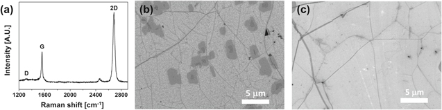
Figure 2. Characterization of CVD-graphene layer grown by two-step process. (a) Raman spectrum of graphene on SiO2. (b) and (c) SEM images of graphene transferred on SiO2 substrate.
Download figure:
Standard image High-resolution imageFigure 3 shows the growth behavior and electrical and optical properties of ALD-In2O3 films. Firstly, figure 3(a) shows the thickness of the In2O3 film as a function of the number of ALD cycles. As typical in the ALD growth, the thickness increased linearly as increasing the number of ALD cycles. A growth rate per cycle (GPC) was 0.042 nm and this value well agrees with our previous results [38]. Figure 3(b) shows the sheet resistance (left) and resistivity (right) of the ALD-grown In2O3 films as a function of the film thickness (10–50 nm). The resistivities of the ALD-In2O3 film were almost constant down to a thickness of 30 nm (∼1.5 × 10⁻³ Ω cm), but it gradually increased up to 3.0 × 10⁻³ Ω cm as the film thickness decreased further down to 10 nm. Apparently, it seems that surface scattering effect became more dominant in the films thinner than 20 nm [40]. The measured Hall mobilities also confirmed this hypothesis, as the analysis showed an almost constant value of mobility (∼45 cm2 V−1 s−1) except that of 10 nm-thick In2O3 (30 cm2 V−1 s−1). Optical transmittances of the In2O3 films are shown in figure 3(d). The In2O3 film exhibited highly transparent characteristics over the visible region and a transmittance of 90.8% or more is obtained when the film thickness was below 30 nm at a wavelength of 550 nm. However, the optical transmittance decreased gradually to 85.3% and 78.0% as the film thickness increased to 40 and 50 nm, respectively.

Figure 3. Characterization of ALD In2O3 film. (a) Thickness of In2O3 film as a function of number of ALD cycles. (b) Sheet resistance and resistivity of ALD In2O3 (c) Hall mobility and sheet carrier concentration of In2O3. (d) Optical transmittance measurement results with respect to thickness of In2O3. Quartz substrate was used as a reference for calibration of the optical transmittance.
Download figure:
Standard image High-resolution imageThen, we studied the electrical and optical properties of the GI-bilayer (figure 4). Figure 4(a) shows the sheet resistance of the GI-bilayer with various thicknesses of the In2O3 films both measured (black dot) and calculated (red dot) based on a parallel resistor model. The reference point (thickness of zero) is also shown for the bare graphene with a sheet resistance of 863 Ω/sq. As the thickness of the In2O3 films increased from 10 to 50 nm, the Rs of GI-bilayer gradually decreased down to 237 Ω/sq. Notably, even the GI-bilayer with the 10 nm-thick In2O3 layer showed a dramatically low Rs (443 Ω/sq) compared to that of the bare graphene (863 Ω/sq). Both the bare 50 nm-thick In2O3 film and the GI-bilayer with the same thickness of In2O3 exhibited Rs values of 251 and 231 Ω/sq, respectively. This indicates the charge conduction was dominated by more electrically conducting In2O3 film in this case.
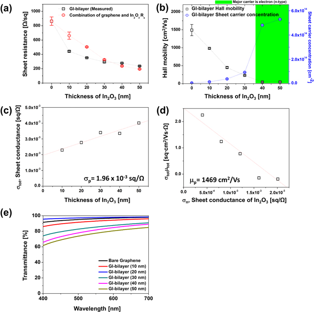
Figure 4. Electrical and optical properties of GI-bilayer. (a) Measured Rs of GI-bilayers as a function of thickness of In2O3 (black). Estimated Rs from values of bare graphene and In2O3 according to the combination of two parallel resistors consisting of graphene and In2O3 are also presented (red). (b) Sheet carrier concentration and Hall mobility of GI-bilayer on the thickness of underlying In2O3 layer. Sheet carrier concentration and Hall mobility of bare graphene are also represented for 0 nm of In2O3. (c) Sheet conductance (σtot) of GI-bilayer according to the thickness of In2O3 film and linear fit to extract sheet conductance of graphene sublayer in GI-bilayer (σp). (d) Plot of σtot·μtot against σn and linear fit to extract mobility of graphene sublayer in GI-bilayer (μp). (e) Optical transmittance of bare graphene and GI-bilayers according to the thickness of In2O3.
Download figure:
Standard image High-resolution imageAssuming that graphene and In2O3 in the GI-bilayer can be considered as two individual resistors, the sheet resistance of GI-bilayer can be considered as that of a parallel series of the two resistors. Therefore, we can calculate the expected Rs of GI-bilayer as a combination of two parallel resistors (i.e. the combination of graphene and In2O3 Rs). The values of each sublayer in GI-bilayer can be taken from the experimentally measured values, namely Rs,Gr = 863 Ω/sq and Rs,In as shown in figure 3(b). The combination of graphene and In2O3 Rs is represented as a red line in figure 4(a). Interestingly, at the low thickness region (10- and 20 nm-thick In2O3), an obvious difference was noted between the measured value (black line) and the combination of graphene and In2O3 Rs (red line). In the case of GI-bilayer with 10 nm-thick In2O3, the measured Rs was 443 Ω/sq and the combination of the graphene and In2O3 Rs values was 661 Ω/sq. This result strongly indicates that the electrical property of graphene sublayer is modified by the underlying In2O3 in GI-bilayer. On the other hand, it seems that the measured Rs value is rather slightly higher than the combination of graphene and In2O3 Rs for GI-bilayer with 40- and 50 nm-thick In2O3. For instance, the estimated and measured Rs of GI-bilayer with 40 nm-thick In2O3 exhibited 237 and 278 Ω/sq, respectively. It would be attributed to contact resistance between graphene and underlying In2O3 sublayer which played a significant role only if the charge conduction was dominated through underlying In2O3 film. The contact resistance of vertical transport between graphene and In2O3 was estimated as 42 Ω by assuming partially connected In2O3 layer with series contact resistances formed in areas lying below the top contacts on the graphene layer [37].
Figure 4(b) shows both the sheet carrier concentration and Hall mobility of GI-bilayer as a function of the underlying In2O3 layer thickness. Hall mobilities of GI-bilayers gradually decreased from 982 to 47.4 cm2 V−1 s−1 as increasing thickness of In2O3. Interestingly, we found that the major carrier in the GI-bilayer changed from the hole (p-type, up to a 30 nm-thick In2O3) to electrons (n-type, for 40- and 50 nm-thick In2O3). The sheet carrier concentration gradually increased from 5.37 × 1012 cm−2 for the bare graphene to 9.31 × 1013 cm−2 for the GI-bilayer with 30 nm-thick In2O3. Then, the majority carrier of GI-bilayer changed from hole to electron as shown in figure 4(b). In this region, the Rs of the In2O3 layer was significantly lower than that of graphene (863 Ω/sq for graphene and 278 Ω/sq for 40 nm of In2O3). The thick In2O3 film dominated the electron conduction of the overall GI-bilayer. As follow, the sheet carrier concentration and Hall mobility of GI-bilayer showed similar values for 40 and 50 nm bare In2O3, as shown in figure 3(c).
The majority charge carrier in each sublayer was different: In2O3 is an n-type material and graphene is a p-type material. Therefore, the electrical properties observed for GI-bilayer should be interpreted as concomitant conduction of electrons and holes in each sublayer. In this point of view, we conducted detail analysis to identify the electrical properties of each sublayer in the GI-bilayer. Similar analysis has been proposed by Bierwagen et al, who determined the electrical properties of a p–n-layer-stacked structure using Hall measurements [41]. They used this model to analyze the electrical properties of p-doped InN, which shows a strong surface electron accumulation layer. Here, the surface accumulation layer works as an n-type conduction path independent of the p-type bulk region [41]. Therefore, this model can be directly used to extract the electrical properties of each sublayer of GI-bilayer. The model provides an estimate of the total sheet conductance (σtot) as the sum of the sheet conductance of the 2-dimensional p-type layer (σp) and that of the bulk n-type layer (σn), as follows:
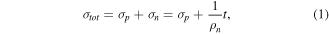
where t and ρn are the thickness and resistivity of In2O3, respectively. σtot is the inverse of the measured Rs of GI-bilayer as shown in figure 4(a). Thus, σtot as a function of t as shown in figure 4(c). One thing has to be addressed is the assumption on the constant resistivity of In2O3 (ρn) in GI-bilayer. We assumed the constant resistivity of In2O3 to apply multilayer Hall measurement model for the GI-bilayer, although resistivity of bare In2O3 films at the low thickness region (from 10- to 20 nm-thick In2O3) exhibited a range of variation. However, as shown in figure 4(c), the values of σtot increased linearly with the constant slope as a thickness of In2O3 increased, and also fitted well with a linear regression model based on equation (1). It means that our experimental data matched well the model given by equation (1) with a constant value of ρn. Further, extracted resistivity of In2O3 based on slope of linear fitting is 2.28 × 10⁻³ Ω cm, which is comparable to that of measured values. These results imply that our assumption on the constant resistivity of In2O3 in the GI-bilayer is valid for multilayer Hall measurement model. On the other hand, the Rs of graphene in the GI-bilayer extracted from the y-intercept of the linearly fitted line in figure 4(c) was 510 Ω/sq. Again, it was confirmed that the Rs of graphene decreased drastically for the GI-bilayer compared to that (863 Ω/sq) of bare graphene.
Table 1. Electrical properties of bare graphene and graphene in GI-bilayer.
| Graphene | Sheet conductance [×10–3 sq Ω−1] | Rs [Ω/sq] | Carrier mobility [cm2 V−1 s−1] | Sheet carrier concentration [×1012 cm−2] |
|---|---|---|---|---|
| Bare graphene | 1.28 | 863 | 1490 | 5.37 |
| Graphene in GI-bilayer | 1.96 | 510 | 1469 | 8.34 |
The sheet carrier concentration and Hall mobility of each sublayer could also be extracted based on Bierwagen's approach [41]. When both electrons and holes work as effective charge carriers in composite materials, the Hall coefficient is expressed using equation (2) and rewritten as a function of sheet conductance (σ) and mobility (μ) as shown by equation (3), where sheet conductance σ = nqμ, and sheet carrier concentration n [41, 42]

where σtot, μtot, and ntot are the measured values of the GI-bilayer, and σp, μp, σn, μn, n, and p are the properties of each p and n-type sublayer. Figure 4(d) shows the linear fitting of σtotμtot as a function of σn based on equation (3). By substituting the σp values given by equation (1), we can easily extract the mobility of graphene in GI-bilayer from the y-intercept for the linear fitting of σtotμtot against σn with Hall effect data for the GI-bilayer. The extracted mobility value of graphene in GI-bilayer was 1469 cm2 V−1 s−1 (figure 4(d)), almost the same as that of bare graphene (1490 cm2 V−1 s−1). In addition, the sheet carrier concentration of graphene in GI-bilayer was obtained from the extracted sheet conductance (figure 4(c)) and Hall mobility (figure 4(d)). The calculated sheet carrier concentration of graphene in GI-bilayer increased from 5.37 × 10¹² (bare) to 8.34 × 1012 cm−2 (in GI-bilayer), as shown in table 1. In other words, graphene in GI-bilayer is p-type-doped by the underlying In2O3, which results in the enhancement of the sheet conductance of graphene in GI-bilayer.
We also measured the optical transmittance of the GI-bilayers for visible light prepared on quartz substrates, as shown in figure 4(e). For each thickness of In2O3, the optical transmittance was observed as simply the sum of the absorption values of bare In2O3 and graphene. With the In2O3 films thinner than 20 nm, we could achieve industrially applicable optical transmittance of the GI-bilayer: more than 93% transparency at a wavelength 550 nm.
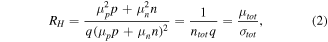
Raman spectroscopy and UPS analysis were further conducted to elucidate the p-type doping of graphene in the GI-bilayer (figure 5(a)). On comparing the positions of the G and 2D bands, a blue shift in the peak position (from 1592 to 1600 cm−1 for G band, from 2722 to 2728 cm−1 for 2D band) was clearly observed. This blue shift was reported for numerous p-type doped graphene[39, 43] and is regarded as a feature of p-type doping of graphene. Therefore, p-type doping of the graphene in the GI-bilayer was double-checked.
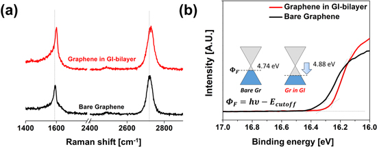
Figure 5. P-type doping on graphene in GI-bilayer. (a) Representative Raman spectrum of bare graphene (black) and graphene in GI-bilayer (red). Perpendicular guidelines indicate peak position of G and 2D bands of the bare graphene. (b) Enlarged UPS spectrum for low-kinetic-energy part of bare graphene and the one in the GI-bilayer. Schematic represents Fermi level shift of the graphene.
Download figure:
Standard image High-resolution imageFurthermore, UPS analysis more directly revealed a change in the electronic energy state of graphene. Figure 5(b) shows the enlarged UPS spectrum of bare graphene and GI-bilayer. UPS can be used to determine the work function by checking the cut-off binding energy since it depends on work function of materials (ΦF = hν − Ecutoff, figure 5(b)). Fermi levels of the bare graphene and graphene in the GI-bilayer were 4.74 eV and 4.88 eV, respectively. This depicts down-shift of the Fermi level due to the p-type doping, which is consistent with Hall measurement results and Raman spectrum. Therefore, it is clear that the hole concentration of graphene in the GI-bilayer increased by the doping and it resulted in the remarkable conductance enhancement of the GI-bilayer.
Reliability of the TCE with a large-area uniform Rs is another major requirement for practical application. In this context, large-area Rs uniformity of GI-bilayer was investigated. Figure 6 shows a histogram and mappings within 7 × 7 cm2 scale of bare graphene and the GI-bilayer. The Rs was measured at 11 × 11 points fairly distributed in the whole area. In the Rs mapping of graphene on SiO2 wafer, some macroscale areas showed a significantly higher Rs compared to the mean value (figure 6(c)) [28, 34]. On the other hand, excellent Rs uniformity of GI-bilayer is indicated by the same color in the contour map and the narrow distribution of the Rs histogram. We also confirmed outstanding Rs uniformity of the GI-bilayer by the standard deviation of Rs and % Rs uniformity, which are listed in table 2. The % Rs uniformity, which is a reliability parameter for practical manufacturing processes, is defined by the following equation [44]
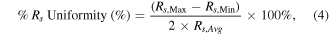
where Rs,Max, Rs,Min, and Rs,Avg are the highest, lowest, and average values of the measured sheet resistance (Ω/sq), respectively. A wide distribution of measured Rs data denotes poor Rs uniformity with a high % Rs uniformity value. In the case of bare graphene, Rs uniformity of 151.1% was noted and this value is about three times higher than the average value. The Rs standard deviation for GI-bilayer decreased by an order of magnitude compared to that bare graphene, from 149.74 to 7.5 Ω/sq. The % Rs uniformity of GI-bilayer also showed a value of only 17.7%, which is acceptable for practical applications. This drastic enhancement in the Rs uniformity can be attributed to the underlying In2O3 layer, which compensated the charge transport degradation on the defects of graphene. The excellent Rs uniformity of GI-bilayer provides another key advantage for practical applications.
Table 2. Areal sheet resistance uniformity of bare In2O3, graphene and the GI-bilayer.
| Material | Rs average [Ω/sq] | Rs standard deviation [Ω/sq] | % Rs uniformity (%) |
|---|---|---|---|
| In2O3 only | 1211.4 | 11.4 | 1.82 |
| Bare graphene | 863.24 | 149.74 | 151.1 |
| GI-bilayer | 353.56 | 7.5 | 17.7 |

Figure 6. Large-area Rs uniformity of the GI-bilayer. Contour map of Rs for (a) bare graphene and (b) GI-bilayer with 20 nm-thick In2O3 underlayer. (c) Rs histogram of bare graphene and the one in the GI-bilayer with 20 nm-thick In2O3.
Download figure:
Standard image High-resolution image
4. Conclusions
In this work, we investigated the electrical and optical properties of the GI-bilayer as a TCE with the improved areal-uniformity. By introducing the In2O3 underlayer, the sheet resistance of graphene decreased significantly from 863 Ω/sq (conventional monolayer graphene) to 510 Ω/sq (graphene in the GI-bilayer). This decrease was interpreted as a result of p-type doping on the graphene induced by the underlying In2O3 layer. Multilayer Hall measurement model, Raman spectroscopy and UPS suggested a clue of p-type doping of graphene in GI-bilayer. More importantly, it should be emphasized that the GI-bilayer exhibited the extreme uniformity on the large-area scale [standard deviation of only 12 Ω/sq over the large area of 49 cm2] owing to the super-uniform ALD-grown In2O3 layer underneath the graphene. Specifically, it was proposed that the In2O3 underlayer acted as a current bypath for a damaged region on the graphene. These results suggest that our GI-bilayer is a promising material that can be used in the fabrication of a highly reliable TCE.
Acknowledgments
This work is supported by the Nano Material Technology Development Program through the National Research Foundation of Korea (NRF) funded by Ministry of Science and ICT (MSIT) of Korea (2015M3A7B4050454, 2017R1D1A1B03035058, and 2019R1A2C2005783). This research was also supported by BioNano Health-Guard Research Center funded by the Ministry of Science and ICT (MSIT) of Korea as Global Frontier Project (H-GUARD_2013M3A6B2078943).