
Abstract
InAs nanowires (NWs) are recognized as a key material due to their unique transport properties. Despite remarkable progress in designing InAs NW device structures, there are still open questions on device variability. Here, we demonstrate that noise spectroscopy allows us to study not only the parameters of traps, but also to shed light on quantum transport in NW structures. This provides an important understanding of structural behavior as well as the background and strategy required to design NW structures with advanced properties.
Export citation and abstract BibTeX RIS

Original content from this work may be used under the terms of the Creative Commons Attribution 3.0 licence. Any further distribution of this work must maintain attribution to the author(s) and the title of the work, journal citation and DOI.
Introduction
InAs nanowires (NWs) have unique properties due to the high mobility of the material and, as a consequence, this allows to demonstrate conductive channels with ballistic conductivity and 1D conductors at appropriate transverse dimensions (tens of nanometers) [1–10]. The violation of conditions for ballistic or 1D transport as a result of molecular binding event to the surface may lead to a radical change in the resistance of nanowires. This effect can be used to develop surface-sensitive field-effect transistor (FET) structures, i.e. biosensors with internal amplification. The formation of 1D conductivity can be determined by the resistance behavior of a sample, taking values that are multiples of the quantum resistance: RK = h/2e2 ≈ 12.9 kΩ [11]. However, under conditions of strong depletion in the channel of a metal-oxide semiconductor (MOS) InAs structure, the resistance reaches hundreds and thousands of kilo-ohms. In these conditions, the detection of quantum conduction effects using I–V characteristics becomes difficult. Therefore, new experimental methods have to be developed. The depletion mode realized at low voltages is especially important for InAs biosensors, since operation at voltages exceeding a certain threshold leads to degradation of both the electrolyte layer and the gate insulator of FET. The latter manifests itself as a voltage-induced capture of free charge carriers by metastable states in a dielectric [12]. In this respect, the operation of NW devices at low voltages is preferable for the detection of small signals of biological objects.
To obtain data on the conductivity behavior of nanowire structures and the fluctuation phenomena several methods can be applied: measurements of I–V characteristics and thermoelectric properties [7–9], as well as noise [4] methods that allow accessing the single-electron random processes, manifested in the form of so-called random telegraph noise (RTS) [13–17]. The latter is a powerful tool for investigating the stochastic and dynamic characteristics of capture and emission processes related to a single trap. In addition, it can also be used to detect molecular charges on the surface of the dielectric layer of a FET structure used as a biosensor (BioFET) [18]. It has been demonstrated that the sensitivity of BioFETs using RTS noise analysis can be increased considerably. Thus, noise spectroscopy can be applied as a highly sensitive tool, indicating the charge state change. At the same time, variability effects influence the electrical characteristics of InAs NW structures, and therefore have to be examined and explained to realize the full potential of the structures and enable the design of devices with predefined properties.
Here, we report on transport and noise properties of InAs nanowire structures. We studied the evolution of the current–voltage (I–V) characteristics and noise parameters of the structures at different temperatures. The data allow us to extract important parameters of traps responsible for RTS noise. On the basis of these data we propose noise spectroscopy as a tool for investigating conduction mechanisms, including quantum phenomena. Thus, the results show the strategy of the investigation of the electronic properties of InAs NW structures, where conductivity is mostly determined by quantum and ballistic mechanisms.
Experimental details
The structures studied are shown schematically in figure 1(a). NWs with diameters of 20 nm were grown using metal organic chemical vapor deposition. Then the NW structures were coated with a 5 nm thick Al2O3 dielectric layer and transferred onto a Si/HfO2 substrate with patterned Ni contacts. The detailed fabrication protocol is described in [9]. It should be noted that the contact resistance is an extremely important parameter determining the device performance [19]. In our case the contact resistance is negligibly small as it was estimated using measurement results of transmission line model (TLM) structures (see [9]).
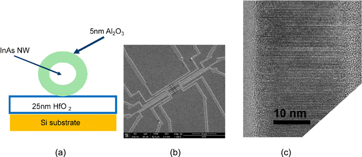
Figure 1. (a) Schematic of NW structures studied, (b) SEM image of one of the InAs nanowire chips, (c) TEM image of one of the InAs nanowires.
Download figure:
Standard image High-resolution imageThe scanning electron microscopy (SEM) image and a high resolution transmission electron microscopy (TEM) image of the InAs NW chip studied is shown in figures 1(b) and (c), respectively. The InAs NW was contacted with several electrodes to measure the transport properties of the NW structures in the TLM. The chip was encapsulated and investigated at different temperatures in the temperature range from 300 K down to 100 K.
We studied three nanowire segments with lengths of 600, 900 and 1200 nm as well as a NW sample with a length of 3 μm. The Si substrate was used as a gate electrode for current flow control. Current−voltage characteristics of the NWs were measured using a Keithley 2400 and 2430 current/voltage measurement units. Both units demonstrate a maximum measurement resolution of 10 pA providing an accurate measurement of both drain-source and gate-source currents. Low-frequency noise characteristics were measured using fully automated ultralow noise measurement setup. The gate-source and drain-source biases were applied to the sample using rechargeable batteries and an ultralow noise variable resistor. The time-dependent source-drain voltage fluctuations were first pre-amplified using an in-house-fabricated ultralow noise preamplifier and then amplified to the measurable range using low-noise amplifier. The noise data collection was performed using U2542A data acquisition module that transfers collected data to a PC via a high-speed USB 2.0 interface. The measured time-dependent source-drain voltage fluctuations were then translated into a voltage power spectral density, SV, in the range from 1 Hz to 100 kHz using fast Fourier transform method. In order to obtain reliable noise characteristics of the samples under study, the number of averages was set at 100 and all measurements were performed in a custom-built Faraday cage to block any external electromagnetic fields.
Results and discussion
In general, nanowire structures demonstrate good scaling and electric properties. This was confirmed by studying the resistance of TLM structures as a function of length [9]. The structures with electron concentrations of about 3 × 1017 cm−3, corresponding to a conductivity of 500 S cm−1 in bulk InAs material [8], demonstrated high mobility values of about 1600 cm2 V−1 s−1 at room temperature. Figure 2 shows typical output characteristics of the InAs nanowire structure with a length of 3.0 μm measured at different gate voltages, VG, in the range from 0 to 2 V at room temperature. The characteristics reflect n-type conductivity behavior. The values of  were averaged over 10 consecutive measurements. It should be noted that the gate leakage current was negligibly small.

Figure 2. Output characteristics of InAs NW with a length of 3.0 μm in (a) linear and (b) double logarithmic scales measured at different gate voltages,  0, 0.25, 0.50, 0.75, 1.00, 1.25, 1.50, 1.75, 2.00 (see inset) at T = 297 K. The dashed line illustrates linear dependence.
Download figure:
Standard image High-resolution imageFigure 3 shows drain current dependence on the back-gate voltage applied to the InAs nanowire biased at different drain-source voltages, VDS, measured at room temperature. The values of  were averaged over 10 consecutive measurements. It can be seen that the dependences
  are linear up to
  At larger
  voltages, the dependences become steeper. Therefore, it can be argued that the measured voltage range corresponds to the near-threshold region.
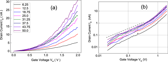
Figure 3. Transfer characteristics of InAs NW with a length of 3.0 μm at different drain voltages, VDS (mV): 6.25; 12.50; 18.75; 25.00; 31.25; 37.50; 43.75; 50.00 plotted in (a) linear and (b) double logarithmic scales, T = 297 K.
Download figure:
Standard image High-resolution imageWe also found that the drain current a little bit decreased at large gate voltages when the device was swept at a lower gate bias sweep rate. Figure 4(a) shows the transfer characteristics measured with different sweep rates. The effect of the gate bias sweep rate on the electronic characteristics can be explained by the contribution of metastable states (with a large time constant) localized at the interface between the InAs core and Al2O3 dielectric shell, which was used as a passivation layer. The slow bias sweep (stationary regime) resulted in depletion of the electrons and in turn caused the reduction in current and carrier density. On the contrary, applying a negative voltage to the gate in slow-sweep mode led to enrichment by electrons and an increase in current with time, as observed in [12]. This effect demonstrates the dependence of the current through the InAs NW sample on the gate voltage in the steady-state mode, as presented in figure 4(a), black curve. The n-type conductivity of the samples was determined using characteristic behavior: increasing drain current with increasing back-gate voltage. The application of a positive voltage to the gate, as in traditional metal-oxide semiconductor FETs (MOSFETs), led to an increase in the number of free electrons and, as a consequence, to an increase in the current in the channel. However, over time, the number of free electrons decreased due to trapping by slow traps in the dielectric. This is a result of increasing capture probability due to a reduced barrier under the action of an electric field in the gate insulator (the Poole–Frenkel effect). This process can be seen in figure 4(b), which shows the I–V characteristics of InAs NWs measured at different temperatures. In order to extract the threshold voltage Vth (V) we used the method of extrapolation from IDS–VG curve in the linear region [20], i.e. in the voltage range VG = (1–2) V (see figure 3(a)).

Figure 4. (a) Transfer characteristics of InAs NW with L = 600 nm measured at fast (black) and slow (red) sweeps, T = 296 K, VDS = 10 mV; (b) the transfer characteristics of 900 nm long InAs nanowire measured at different temperatures (indicated on the inset), VDS = 10 mV.
Download figure:
Standard image High-resolution imageAs can be seen in the graph, as the temperature decreases, the effect of capturing free carriers on the traps in the dielectric decreases, demonstrating the influence of thermo-activation mechanism.
A distinctive feature of the material studied here is the high mobility of free charge carriers. We determined the mobility of InAs NW electrons from the transfer characteristics at different temperatures. The effective mobility was determined at maximum transconductance using transfer characteristic measured at VDS equal 25 mV. Oxide capacitance, COX, was calculated taking into account the cylindrical shape of the nanowire. For the calculation we used literature values of dielectric constant for HfO2 equal to 18 and for Al2O3 equal to 3.9. The results are shown in figure 5(a). As can be seen, the value of mobility increased at a temperature of 220 K and approached a value of about 2500 cm2 V−1 s−1. The high mobility values reflect the good quality of the NW samples and are in agreement with data reported in the literature [9]. We registered a tendency towards decreased mobility at temperatures T < 170 K and at T > 270 K due to changes in dominant scattering mechanisms.

Figure 5. (a) Temperature dependence of the mobility, determined using measured ID(VG) characteristics for 3.0 μm long InAs NW sample; (b) the conductance of 3.0 μm length InAs NW as the function of the gate voltage, measured at VDS = 25 mV and temperature T = 120 K. The sequence of several repeated sweeps was shifted for clarity and shown in the inset.
Download figure:
Standard image High-resolution imageSingle-electron phenomena
Figure 5(b) shows the conductivity dependence on the voltage applied to the gate, VG, taken at three different sweeps and measured at T = 120 K. The curves practically coincide, except for the instability regions between 0.5 and 0.8 V. The instabilities reflect transitions between two definite discrete levels. The transitions are registered at approximately the same voltages VG. It can be concluded that at the temperatures below than 120 K metastable centers with long lifetimes that cause jumps in drain current are activated mainly by voltage rather than by temperature. This reflects the fact that transitions occur between centers with approximately the same energies, but over relatively large distances, in accordance with the theory of hopping conductivity with variable hopping length [21].
It should be noted that RTS fluctuations with large time constants are registered in a certain voltage range in the steady-state regime, namely where the jumps in current are observed (in figure 5(b), the range is  ). The low probability of transitions (a large time constant) indicates that transitions between spatially-spaced states predominate at relatively low temperatures. This fact again demonstrates a significant width of the depletion region under the surface dielectric due to the presence of spatial quantization.
The dependence of the conductance of the 3 μm long nanowire on the gate voltage is shown in figure 6(a) for different temperatures. The non-monotonicity of the changes in the position of the curves with temperature can be clearly seen, i.e. an abrupt change in the conductance with a change in temperature.

Figure 6. (a) The conductance of the sample with length L = 3 μm as a function of the gate voltage, measured during the first voltage sweep at VDS = 10 mV and different temperatures; (b) the temperature dependence of the conductance in the NW sample measured at different VG, at  during the first sweep measurement with minimum drift.
Download figure:
Standard image High-resolution imageA more detailed analysis of the temperature dependences for several voltage values as a function of the gate voltage VG is shown in figure 6(b). As can be seen in figure 6(b), a number of conductance levels can be distinguished and are labeled in the figure from a to n.
A quite significant amplitude of the current jumps is registered (see figure 7(a)). The relative amplitude of the current (ratio) can reach a value of 0.96 in the channel. No dependence on temperature was observed. The typical value of the ratio was found to be ∼0.25. At T = 210–220 K, relatively large scattering in data was measured.
Figure 7. (a) The relative amplitude of current jumps in the NW sample with length L = 3 μm, obtained at different temperatures; (b) temperature dependence of the number of conduction electrons in a channel of the sample with length L = 3 μm obtained for two values of the voltage VG (shown in the inset).
Download figure:
Standard image High-resolution imageThe stepwise behavior of the temperature dependences can be explained by an increase in the number of free electrons in the channel, or a change in the number of parallel channels (quantum modes) of conductivity through the nanowire as a result of the capture/emission of electrons and the increase in the temperature. Since the probability of an electron passing through one mode in the channel is less than unity, this mode of conductivity acts as a quantum barrier. The fact that we are dealing with single electrons is evidenced by a calculation showing that the number of electrons must be countable: from ∼1 at low temperatures to 13–15 electrons with increasing of temperature at VG = 0 (see figure 7(b)).
The quantum nature of the conductivity assumed in the samples is due to a diameter which is of the order or smaller than the de Broglie wavelength:

where  is the kinetic energy of the electron:
 is the rest mass,
  is the effective mass of the electron. The energy is equal to
  and
and  at room temperature and T = 100 K, respectively. Taking into account that the effective mass of the electron in InAs at low impurity concentrations is
  the de Broglie wavelength is estimated using equation (1) to be 154 nm at room temperature and 272 nm at T = 100 K. Thus, the diameter of the InAs nanowires studied (20 nm) is much smaller than these values, which implies the presence of a one-dimensional conductivity in the nanowires.
In addition, temperature dependence of threshold voltage (see figure 8(a)), obtained for samples of different lengths, reflects non-trivial behavior as a function of sample length. This can also be explained by the tendency of 1D conductivity formation and supports the estimations.

Figure 8. (a) Threshold voltage as a function of temperature, obtained for InAs NW samples of different lengths at different temperatures at VDS = 25 mV; (b) noise spectra of InAs NW segment (L = 600 nm), measured at different back-gate voltages in the range: VBG = (−0.3)–(1.0) V and VDS = 10 mV, T = 297 K.
Download figure:
Standard image High-resolution image1D transport was confirmed by the results of noise spectroscopy data, as it will be shown below.
Noise spectroscopy
The noise measurement results are shown in figure 8(b). The measured noise spectra of InAs nanowires demonstrated 1/f behavior (flicker) noise with intensity depending on the back-gate voltage. However, several Lorentzian components related to random telegraph signal noise (discussed below) can be resolved in the noise spectra of InAs nanowires.
The current spectral density of the 1/f noise, SI, as a function of drain current, IDS, is usually described by Hooge's empirical relation [22]:

where f is the frequency,  is the dimensionless Hooge's parameter and N is the total number of free charge carriers (
 ). After some transformations, the expression for
  can be presented in the form:
where  is the drain-source voltage, R is the sample resistance, q is the electron charge,
  is the electron mobility in the sample. The
  dependences on the current are shown in figure 9(a) for three samples at a frequency f = 10 Hz at a temperature T = 150 K. Note that at this temperature, 1/f components dominate in the noise spectra at the low frequencies. Therefore, the representation of
  is correct here. Unlike samples of length L = 900 nm and L = 1200 nm, a sample of length L = 600 nm demonstrates substantially smaller values of
  approaching the typical value
  and depends only slightly on the drain current. This reflects the fact that noise is predominantly determined by scattering in current-conducting bulk regions of the contacts in this case, and the electrons are not scattered in the sample itself due to their ballistic motion.

Figure 9. (a) Current dependences of  samples of different lengths at temperature T = 150 K, obtained at frequency f = 10 Hz and voltage on samples
  = 10 mV; (b) typical time trace of random telegraph signal noise observed in the InAs NW samples, T = 297 K.
Download figure:
Standard image High-resolution imageSeveral Lorentzian components can be found in the noise spectra. For these components, the characteristic time constant is determined as:

where  and
and  are the mean time corresponding to the capture and emission current levels (figure 9(b)), respectively.
We first estimated parameters of RTS noise that was observed in an InAs nanowire with a length of 1200 nm. The results are shown in figure 10. The emission time constant  does not depend on gate voltage and
  demonstrates a weak dependence on the gate voltage applied to the sample (see figure 10(a)). Such behavior indicates that the trap center is located in the region where the concentration of free carriers is independent of gate voltage changes.

Figure 10. (a)  and
and  time constants as a function of the back-gate voltage applied to the InAs nanowire with a length of 1200 nm, T = 297 K. (b) The amplitude of RTS noise as a function of gate voltage measured for the same sample at VDS = 10 mV.
Download figure:
Standard image High-resolution imageRTS fluctuations are observed mainly at temperatures above T = 180 K. At lower temperatures, only 1/f noise appears in the investigated frequency range (see figure 11(a)). Generation-recombination fluctuations (in the form of RTS fluctuations) do not appear in the noise spectra because their time constants are too large, although such oscillations are present visually on the oscillogram.

Figure 11. (a) Temperature dependence of the spectral density of the normalized current noise of a sample with length L = 3 μm at a frequency f = 1 Hz, obtained at VG = 2 V and VDS = 10 mV; (b) Arrhenius plot, obtained using noise spectra measured for the sample of L = 1200 nm.
Download figure:
Standard image High-resolution imageThe disappearance in the RTS noise spectra of high-frequency components with time constants τ < 1 s at temperatures T < 200 K may indicate the presence of a barrier at the InAs/Al2O3 interface whose height and/or width increases with decreasing temperature. This is probably a consequence of the increased role of electron quantization in energy and the formation of the 1D channel due to the enhancement of confinement with decreasing temperature.
We then determined the activation energy of the traps using an Arrhenius plot. Figure 11(b) shows the temperature dependences of  where τ is the time constant of the generation-recombination (GR) process. The energy depths of the active traps were determined. Well-defined donor traps with an energy
  and
and  were different. The activation energies of the third level (red circles on figure 11(b)) with an energy of 360 meV is very close to the value of the InAs bandgap (indicated by the dotted line in figure 11(b)), suggesting the presence of band-to-band transitions or transitions between small acceptor levels near the top of the valence band and the bottom of the conduction band.
The obtained activation energies agree well with the literature data [23]. In addition, we registered several GR noise components. Surprisingly, the parameters of the components changed synchronously. This indicates the presence of quantized states in the conduction band with the same trap exchanging an electron with several states.
The characteristic length for 1D transport can be estimated as follows. For a concentration in the NW channel of  which remains almost constant with temperature, the Fermi wavelength can be obtained using the following relations:
  Using
Using  =
=  then
then  Thus, for a nanowire diameter of 20 nm, the quantization effect can be registered In this respect, our data on noise spectroscopy provide direct information on the formation of well-separated quantized levels in the structure and on exchange processes between these levels and single trap positioning near the InAs/dielectric interface.
Figure 12 shows a number of τ (VG) characteristics and the low-frequency Lorentzian noise plateau values, SI(0). The data reflect capture/emission processes related to several active centers (depicted as 1–5) present in an InAs nanowire structure with a length of 600 nm.

Figure 12. (a) The time constant of capture-emission processes as a function of gate voltage, obtained for the NW sample of L = 600 nm; (b) the low-frequency Lorentzian noise plateau values, SI(0), extracted from measured noise spectra, as a function of gate voltage. T = 297 K.
Download figure:
Standard image High-resolution imageThe Lorentzian noise, reflecting GR processes  can be described using the following relation:
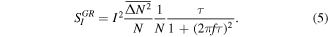
As can be derived from the equation (5),  changes are related to changes in
  This means that the amplitude of the relative dispersion
  for each Lorentzian component in the noise spectrum decreases with an increasing charge carrier number N.
The probability of such transitions differs, as confirmed by the difference in the time constants under equal conditions. As can be seen in figure 12, the time constants corresponding to transitions between the bottom of the conduction band and the neighboring quantum states differ by almost one order of magnitude. The results can be explained within the following model.
The model representation of the band structure with the quantum levels is shown in figure 13. The Fermi level shifts with the application of voltages to the gate and/or channel, which leads to a change in the conditions for electron exchange between the levels. The bottom of the conduction band for the non-quantum case is the level E = 0.

Figure 13. Schematic representation of the band structure with quantum levels for 1D conductivity in a NW sample.
Download figure:
Standard image High-resolution image
Under the influence of gate voltage or temperature, the population of the quantum levels E1–E4 changes. As a result of such redistribution of the carriers the number of conduction channels N varies and the conductivity of the sample changes abruptly (see figure 9), respectively. The jumps in the conductivity change determines by the fact that each channel has a quantum conductivity  where R is the reflection coefficient of the electron wave from the contacts. The total conductivity in this case is equal to:

The coefficient  can take values in the range of 0 <
  depending on the energy of the electrons, the specific quantum level and the degree of scattering. For this reason, the distances between the discrete levels of conductivity (see figure 6) change accordingly.
Conclusion
The transport and noise properties of high-quality InAs NW samples of different lengths were studied in a wide temperature range down to 100 K. Non-trivial behavior of the temperature dependence of the threshold voltage was explained by the tendency of 1D conductivity formation. Our results on noise spectroscopy provide important information for confirming the formation of 1D conductivity at room temperature with a particularly strong quantization effect in the low-temperature range. In addition, the activation energies of the active traps causing fluctuations were determined as 50 and 100 meV. The traps are responsible for increased noise levels at temperatures above 200 K and an increasing drain current. A model was proposed to explain the registered effect of the synchronous change in the parameters of the Lorentzian noise component. Our results demonstrate that operational regimes with low current are preferable to exploit the full potential of quantization effects in the channels of InAs NW structures.
Acknowledgments
Y Kutovyi greatly appreciates a research grant from the German Academic Exchange Service (DAAD). Authors acknowledge Lynne M Gignac from IBM Thomas J Watson Research Center for high resolution TEM image of InAs nanowire structure.