

Abstract
In this paper, we study intersubband characteristics of GaN/AlN and GaN/Al0.4Ga0.6N heterostructures in GaN nanowires structurally designed to absorb in the mid-infrared wavelength region. Increasing the GaN well width from 1.5 to 5.7 nm leads to a red shift of the intersubband absorption from 1.4 to 3.4 μm. The red shift in larger quantum wells is amplified by the fact that one of the GaN/AlN heterointerfaces (corresponding to the growth of GaN on AlN) is not sharp but rather a graded alloy extending around 1.5–2 nm. Using AlGaN instead of AlN for the same barrier dimensions, we observe the effects of reduced polarization, which blue shifts the band-to-band transitions and red shifts the intersubband transitions. In heavily doped GaN/AlGaN nanowires, a broad absorption band is observed in the 4.5–6.4 μm spectral region.
Export citation and abstract BibTeX RIS
1. Introduction
Semiconductor nanowires, at the forefront of device miniaturization, have already seen a wide range of successful applications in chemical and biological sensing, optoelectronics and electronic devices [1–4]. Nanowire research is driven by their potential advantages, such as their small electrical cross section and large surface-to-volume ratio, which allows elastic relaxation of the misfit strain, hence extending the range of possibilities for the device designer.
In spite of a number of demonstrations of resonant electron transport in heterostructured nanowires [5–10], their application in the domain of intersubband optoelectronics remains relatively unexplored. In these devices, nanowires have been proposed as a way to independently control the electrical and the optical device cross section by changing the nanowire density [11, 12]. Also, three-dimensional (3D) confinement of carriers opens up new possibilities to control carrier relaxation times [13, 14]. Intersubband absorption was demonstrated in GaN/AlN multi-quantum-wells grown on self-assembled GaN nanowires [15, 16]. The transitions were broad though, with a full width at half maximum of 400 meV, and were limited to the short-wavelength infrared region even for large GaN quantum disks, due to strong many-body effects. Ajay et al [17] studied the effect of doping and dopants (Si- and Ge- doping) on the intersubband absorption of GaN/AlN heterostructures on GaN nanowires reporting narrower absorption linewidths, around 250 meV. The first demonstration of an intersubband photodetector in a single nanowire was reported by Lähneman et al [18] using the same GaN/AlN material system. When excited with a laser at 1.55 μm, the device displayed a photocurrent that scaled linearly with the impinging laser power. More recently, Karimi et al [19] reported the first intersubband photodetector using a nanowire ensemble as active region. In their case, the active heterostructures consisted of InAsP quantum disks on InP nanowires, and the photocurrent spectrum peaked at 12.4 μm.
Infrared absorption at room-temperature was also reported in InGaN/GaN nanowire heterostructures [20], although its atribution to intersubband absorption is not clear. Also in planar layers, the observation of intersubband absorption in InGaN/GaN structures proved more challenging than in the case of GaN/AlGaN, due to the difficulty to synthesize homogeneous InGaN alloys and chemically sharp InGaN/GaN interfaces [21, 22]. As a result, research on intersubband optoelectronics using III-nitrides has focused on the GaN/(Al, Ga)N material combination.
The GaN/AlN material combination remains highly interesting due to the possibility to cover a broad range of the infrared spectrum [23–27], including the short-wavelength infrared (1–3 μm), mid-infrared (3–5 μm) and far-infrared (15–1000 μm). However, the observation of intersubband absorption in GaN/AlN nanowire heterostructures is so far limited to 1.3–1.95 μm. It is hence important at this point to venture to longer wavelengths. To this end, we propose either by using larger quantum wells or by using AlGaN ternary alloys as quantum well barriers, thus reducing the internal electric field in the wells.
In this paper, we demonstrate intersubband absorption in GaN nanowires with GaN/(Al, Ga)N heterostructures structurally designed to absorb in the mid-infrared wavelength region. To obtain a red shifted intersubband transition, we follow two approaches, the first one involving increasing the GaN well width in GaN/AlN heterostructures from 1.5 to 5.7 nm, which leads to a shift of the intersubband absorption from 1.4 to 3.4 μm. Through the second approach, we demonstrate intersubband absorption in GaN/Al0.4Ga0.6N heterostructures, thereby reducing the effects of polarizations, which shifts the intersubband transitions to cover the mid-infrared spectral range from 4.5 to 6.4 μm.
2. Methods
The design of the samples is performed using the nextnano3 8-band k · p Schrödinger–Poisson equation solver [28], with the material parameters described in [29]. We compare the results of 1D and 3D calculations. For 1D calculations, we considered three periods of the multi-quantum-well, with periodic boundary conditions. The structure was assumed biaxially strained in such a way that the in-plane lattice parameter corresponds to the lattice parameter a of an AlGaN layer with an Al mole fraction equal to the average Al content of the GaN/(Al, Ga)N heterostructure. For the 3D calculations, the nanowire was defined as a regular hexagonal prism with minor radii being 20 nm. In length, it consisted of a 100 nm long base GaN section, followed by 20 periods of GaN/(Al, Ga)N quantum wells, and a 30 nm thick GaN cap. This cap layer was designed to reduce the sensitivity of the structure to the surface states of the (000-1) top nanowire surface. The difference in polarization between the GaN cap and the underlying multi-quantum-well results in a negative charge sheet at the (Al, Ga)N/GaN cap interface, which favors the accumulation of electrons at that point regardless of the degree of occupancy of the surface states. The GaN base and the GaN/AlN heterostructure were laterally surrounded by a 5 nm thick AlN shell (2 nm thick AlN in the case of the GaN/Al0.4Ga0.6N heterostructure), and the whole nanowire structure was enclosed in a rectangular prism of air, permitting elastic deformation. The 3D strain distribution is calculated by minimization of the elastic energy assuming zero stress at the nanowire surface.
Self-assembled (000-1)-oriented GaN nanowires were synthesized on floating-zone Si(111) substrates using plasma-assisted molecular beam epitaxy (PAMBE) under nitrogen-rich conditions. The growth started with the deposition of an AlN buffer using a two-step procedure, as described elsewhere [30]. Then, a 700 nm long GaN base was grown under N-rich conditions (Ga/N flux ratio = 0.25), at a substrate temperature TS = 810 °C, and with a growth rate of 330 nm h−1. This was followed by the active region, consisting of a GaN/(Al, Ga)N multi-quantum-well, where the GaN wells were grown using the same N-rich conditions as for the GaN base, and the (Al, Ga)N sections were grown at the stoichiometry. A 2 nm section in the center of the GaN quantum wells was doped with Si at various concentrations. The calibration of the dopant density was performed by Hall effect characterization using the Van der Pauw method on Si-doped GaN planar layers. Finally, the active region was capped with 30 nm of GaN, which is also grown under N-rich conditions.
The structural quality was analyzed by x-ray diffraction (XRD) using a Rigaku SmartLab x-ray diffractometer using a 4 bounce Ge(220) monochromator and a Si compensator. The morphology of the as-grown nanowire ensemble was studied by field-emission scanning electron microscopy (SEM) using a Zeiss Ultra 55 or a Zeiss 55 microscope. Detailed structural studies were conducted using high-angle annular dark-field scanning transmission electron microscopy (HAADF-STEM) performed on a probe-corrected FEI Titan Themis microscope operated at 200 kV.
Low-temperature (T = 5 K) photoluminescence (PL) spectra were obtained by excitation with a frequency doubled Ar+ laser (λ = 488 nm), with an optical power of ≈5 μW focused on a spot with a diameter of ≈100 μm. The emission from the sample was collected by a Jobin Yvon HR460 monochromator equipped with an ultraviolet-enhanced charge-coupled device camera. Room-temperature Fourier transform infrared spectroscopy (FTIR) was used to probe the intersubband absorption using a halogen lamp, a CaF2 or KBr beam splitter, and a mercury-cadmium-telluride detector incorporated into a Bruker V70v spectrometer.
3. Results and discussion
The aim of this study was to explore the possibility to extend the intersubband transitions in GaN-based nanowire heterostructures from the near-towards the mid-infrared domain. With this purpose, we first analyzed the potential to red shift the absorption of GaN/AlN quantum wells by increasing the GaN well width. Then, we extended our work to GaN/AlGaN, where the use of a ternary alloy results in a reduction of the axial internal electric field. The samples under study, their dopant concentration, Al content in the barriers, and other structural/optical properties are listed in table 1. Three different nominal architectures were considered:
- (i)samples A1–A3 in table 1 consisted of 30 periods of GaN/AlN (4 nm/3 nm) quantum wells,
- (ii)sample B1 contained 19 periods of GaN/AlN (6 nm/3 nm) quantum wells, and
- (iii)samples C1–C3 consisted of 30 periods of GaN/Al0.4Ga0.6N (4 nm/3 nm).
Table 1. Structural and optical characteristics of the nanowire heterostructures: Al concentration in the barriers, Si concentration in the 2 nm doped region in the quantum wells, multi-quantum-well period (GaN + AlN) measured by XRD, GaN width estimated from the XRD and TEM measurements, PL peak wavelength with error bar representing the spectral width at 90% of the maximum intensity, theoretical calculation of the e1−h1 transition in the wells at 5 K using the nextnano3 software in 3D, IR absorption peak wavelength with error bar representing the spectral width at 90% of the maximum absorption, theoretical calculation of the e1−e2 transition in the wells using the nextnano3 software in 1D.
| Sample | Al (%) | [Si] (cm−3) | Period (nm) | GaN width (nm) | PL peak (nm) | e1–h1 3D (nm) | IR absorption peak (μm) | e1−e2 1D (μm) |
|---|---|---|---|---|---|---|---|---|
| NS1 | 100 | 3 × 10¹⁹ | 4.6 ± 0.2 | 1.8 ± 0.2 | 339 ± 4 | 325 | 1.55 ± 0.11 | 1.72 |
| NS2 | 100 | 1 × 10²⁰ | 4.3 ± 0.2 | 1.7 ± 0.2 | 338 ± 3 | 323 | 1.41 ± 0.11 | 1.63 |
| A1 | 100 | 1 × 10¹⁹ | 7.0 ± 0.3 | 3.7 ± 0.3 | 445 ± 9 | 453 | 1.74 ± 0.13 | 2.21 |
| A2 | 100 | 3 × 10¹⁹ | 6.3 ± 0.2 | 3.3 ± 0.2 | 412 ± 5 | 422 | 1.87 ± 0.13 | 2.18 |
| A3 | 100 | 1 × 10²⁰ | 6.8 ± 0.2 | 3.7 ± 0.2 | 430 ± 12 | 425 | 1.78 ± 0.12 | 2.18 |
| B1 | 100 | 1 × 10¹⁹ | 8.6 ± 0.2 | 5.7 ± 0.3 | 490 ± 19 | 562 | 3.4 ± 0.5, 1.45 ± 0.13 | 2.6 |
| 504a | 3.0a | |||||||
| C1 | 40 | 1 × 10¹⁸ | 6.2 ± 0.2 | 3.7 ± 0.4 | 368 ± 3 | 358 | — | 4.9 |
| C2 | 40 | 1 × 10¹⁹ | 6.6 ± 0.2 | 4.0 ± 0.4 | 365 ± 3 | 365 | — | 4.8 |
| C3 | 40 | 1 × 10²⁰ | 5.7 ± 0.3 | 3.7 ± 0.4 | 362 ± 2 | 351 | 6.4–4.5 | 4.6 |
aIntroducing 2 nm of graded alloy at the bottom interface of the well.
The reduction in the number of periods in (ii) aimed at keeping the active region thickness approximately constant.
For comparison purposes, table 1 contains also samples NS1 and NS2 containing a GaN/AlN multi-quantum-well with similar AlN barriers (≈2.7 nm) and thinner GaN wells (1.7 and 1.8 nm, respectively). Detailed characterization of these two samples can be found in [17]. Note that samples A1–A3 present similar geometry than S1–S4 in [16], presenting intersubband absorption in the 1.60–1.95 μm range. However, we have significantly reduced the doping level, in an attempt to reduce the spectral blue shift of the intersubband absorption due to many-body effects. Note that the surface doping density in [16] was 3.6 and 12 × 1013 cm−2 (using Ge as a dopant), to be compared with 0.2–2 × 1013 cm−2 in this work (using Si as a dopant).
3.1. Structural properties
Figure 1 presents tilted (≈45°) SEM images of samples A1 and C1, containing GaN/AlN and GaN/AlGaN multi-quantum-wells, respectively. The images present the typical morphology of self-assembled GaN wires grown by PAMBE, without bending or deformation of the nanowire shape due to the presence of the heterostructures. HAADF-STEM images of the active region of samples A1, C2 and B1 are presented in figure 2. In the case of the GaN/AlN multi-quantum-well with 4 nm thick GaN wells (A1, in figures 2(a) and (b)), the well/barrier interfaces are chemically sharp, and we observe the presence of a ≈5 nm thick AlN shell surrounding the GaN/AlN heterostructure (see figure 2(b)), which has been commonly observed on such nanowire heterostructures before [31–33], and is due to the low mobility of Al atoms on the nanowire sidewalls at the growth temperature [34]. The shell thickness gradually decreases as we move towards the cap. The first two or three quantum wells are characterized by a narrower width and higher irregularity in the thickness, which can deviate up to two monolayers (±0.5 nm) from the average. The broadening of the disks occurs during the growth, in an attempt to partially relieve the strain induced by the lattice mismatch between AlN and GaN. The first quantum wells are grown under different misfit stress conditions: the GaN stem, which is originally relaxed, becomes compressively strained along the growth axis during the growth of the quantum wells, due to the formation of the AlN shell [35]. The strain stabilizes after the growth of about 3 multi-quantum-well periods [16, 36], which leads in turn to the stabilization of the well width and diameter. Depending on the growth conditions, misfit stress can lead to well/barrier intermixing [36], but it is not the case in the samples under study.

Figure 1. Tilted (45°) SEM images of samples (a) A1 and (b) C1.
Download figure:
Standard image High-resolution image
Figure 2. HAADF-STEM images and corresponding intensity profiles of the active region of a nanowire from samples (a), (b) A1, (c)–(f) C2 and (g), (h) B1. Dark/bright contrast corresponds to Al-rich/Ga-rich areas. The '*' symbol in (f) indicates a region of higher intensity corresponding to increased Ga content in the AlGaN barrier.
Download figure:
Standard image High-resolution imageIn the case of GaN/AlGaN (e.g. sample C2 in figures 2(c)–(f)), the nanowires also present an Al-rich shell that envelops the quantum wells and the stem. This shell is thinner (about 3 nm at the stem/multi-quantum-well interface) than in the case of the wells with AlN barriers, and its Al composition is higher than that of the barriers, although it is difficult to determine precisely. The ternary compound represents a reduction of misfit in comparison to AlN. Therefore, the diameter and width of the GaN wells is more homogeneous along the structure. However, the image contrast reveals certain composition inhomogeneities in the barriers. In some barriers we observe a brighter region in the center indicating a Ga-rich region (see the '*' labeled region in figure 2(f)). Moreover, near the nanowire sidewall, we first find a dark contrast followed by a brighter contrast in the AlGaN barrier indicating radial composition inhomogeneities (see bottom region of figure 2(d)).
Finally, figures 2(g) and (h) present HAADF images of sample B1, the GaN/AlN heterostructure with ≈6 nm GaN wells. From the intensity profile in the inset of figure 2(h) we see that the interface of AlN grown on GaN is sharper than the interface of GaN grown on AlN, which extends by around 1.5–2 nm. Note that this asymmetry can influence the confinement of carriers in the well, as it will be discussed later.
Asymmetry at the interfaces, involving intermixing or alloying, is often found in GaN/AlN multi-quantum-wells in nanowires with large wells, and it is explained by the strain evolution of GaN during the growth process [36]. Indications of graded GaN/AlN interfaces are also reported in Ga-polar GaN/AlN quantum wells grown by metalorganic vapor phase epitaxy [37], and are attributed to the instability of the GaN/AlN interface under strain [38]. In this latter case, it is possible to attenuate the interdiffusion by forcing a compressive strain in the layers [37] and reducing the growth temperature [39], which can be combined with a pulsed injection process [40]. However, in the case of nanowire growth, such tuning of the growth conditions leads also to modifications of the nanowire diameter and shape.
The average thickness of one period of the GaN/(Al, Ga)N multi-quantum-well structure was extracted from the inter-satellite angular distance of the XRD θ–2θ scan around the (0002) reflection. The results are listed in table 1, and exemplary diffractograms of samples A1, C3, and B1 are shown in figure 3, together with simulations using the Rigaku HRXRD plugin of the SmartLab Studio II software. The simulations considered planar layers with the structural parameters of the multi-quantum-wells in table 1, and their strain state was considered as the only fitting parameter. The GaN width indicated in the table is an estimation based on the statistical analysis of HAADF-STEM images of selected samples.
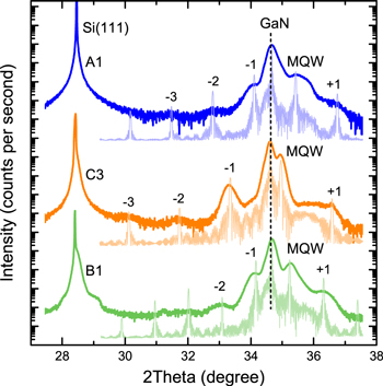
Figure 3. XRD θ−2θ scans of samples A1, C3 and B1. The scans are vertically shifted for clarity. Lighter shades are simulated data. Labels indicate the (111) reflection of the Si substrate, the (0002) reflection of the GaN stem, and the (0002) reflection of the multi-quantum-well (MQW), with several satellites.
Download figure:
Standard image High-resolution image3.2. Band-to-band optical characterization
We analyzed the band-to-band behavior of these samples by low-temperature PL at 5 K. The PL peak wavelengths are summarized in table 1. As an example, the inset of figure 4(a) presents the PL spectra of samples NS1, A1 and B1, illustrating how the emission red shifts with increasing quantum well width in GaN/AlN heterostructures. In most of the samples (e.g. A1 in the inset of figure 4(a)), a weak PL emission from the GaN stem is visible at around 360 nm (3.44 eV). This indicates that the stem is significantly strained due to the AlN shell, as the unstrained GaN emits rather at 357 nm (3.47 eV).

Figure 4. (a) Theoretical value of the e1−h1 transition in GaN/AlN nanowires with varying well thickness, calculated using the nextnano3 software in 3D (solid lines) and 1D (dashed lines). Data points indicate the PL peak wavelength of the samples under study, with horizontal error bars representing the uncertainty in the well thickness and vertical error bars representing the spectral width at 90% of the maximum PL intensity (simulations and experimental data at 5 K). Inset: normalized low-temperature (5 K) PL spectra of samples NS1, A1 and B1. (b), (c) Calculations of the band diagram of a GaN/AlN multi-quantum-well structure with the dimensions of B1, presenting (b) sharp GaN/AlN interfaces, and (c) a 2 nm graded interface (first interface of the well along the [000-1] growth axis). The squared wavefunctions for the three first electron levels (e1, e2, e3) and the first hole level (h1) are also represented. The calculations were made in 1D using the self-consistent 8-band k · p Schrödinger–Poisson solver of nextnano3.
Download figure:
Standard image High-resolution imageIn figure 4(a), the peak emission wavelength of the GaN/AlN samples under study is compared with theoretical calculations. Note that the experimental points are plotted with a horizontal error bar that represents the error in the determination of the GaN well width, and a vertical error bar that indicates the spectral width at 90% of the maximum intensity. Theoretical calculations were performed in 1D (dashed lines) and 3D (solid lines) for various doping levels, indicated by different colors. In general, the result of 3D calculations deviates slightly from the 1D approximation due to the strain distribution in the wire, particularly to the effect of the compressive stress along the nanowire axis imposed by the presence of the AlN shell. Increase in doping for the same quantum well dimensions results in blue shifting of the PL emission due to screening of the internal electric field. For higher doping levels, the deviation between 1D and 3D calculations becomes more significant, since it is easier to screen the internal electric field in the nanowire geometry, as previously demonstrated [41, 42].
The experimental points match the theoretical calculations within their error bars, with the exception of sample B1, emitting at 490 ± 19 nm, which is far from the 562 nm theoretically predicted. The explanation to this discrepancy is found looking back at the structural characterization of the sample. Figures 2(g) and (h) showed that the first interface of the well along the growth axis presents a GaN-AlN intermixing area that can extend 1.5–2 nm. To visualize the effect of such an interface on the band diagram, figures 4(b) and (c) presents 1D calculations of the band diagram of a GaN/AlN multi-quantum-well structure with the dimensions of B1. We compare a structure (b) with sharp GaN/AlN interfaces and (c) with a 2 nm graded interface (first interface of the well along the growth axis, in agreement with our observations). The squared wavefunctions for the three first electron levels (e1, e2, e3) and the first hole level (h1) are also displayed in the figure. Due to the sign of the electric field in the wire, the graded interface corresponds to the area of highest probability of localization of the electrons within the well. Therefore, the shape of the electron wavefunctions is very sensitive to the interface quality. As the interface gets broader, the electron and hole wavefunctions get closer along the growth axis and the e1−h1 transition energy blue shifts. Considering the geometry of B1, the theoretical wavelength associated to the e1−h1 transition becomes 504 nm (see table 1), now within the error bar of the experimental value (490 ± 19 nm).
In the case of GaN/AlGaN heterostructures (samples C1–C3 in table 1), their emission spectra are clearly blue shifted with respect to GaN/AlN samples of similar dimensions (PL peaks between 362 and 368 nm for samples C1–C3, to be compared with peaks between 430 and 445 nm for samples A1–A3), due to the reduction in the internal electric field when lowering the Al content. The experimental emission wavelength shows good agreement with 3D calculations of the electronic levels, as shown in table 1.
3.3. Intersubband optical characterization
Room-temperature FTIR spectroscopy was used to study the intersubband absorption in these heterostructures. The optical transmission of the samples was measured at various angles of incidence (defined with respect to the sample surface), and an infrared polarizer was used to discern between the transverse-electric (TE) and transverse-magnetic (TM) polarized light. Transmission dips assigned to intraband absorption appear only at grazing angles between 5° and 20° and for TM-polarized light. To correct the spectral variation of the light intensity and the effect of the substrate, spectra are divided by the transmittance of a reference sample containing undoped GaN nanowires with the same total length as samples in table 1. The transmittance of this reference sample is very similar to that of the samples with GaN/(Al, Ga)N heterostructures when measured at larger angles of incidence (30°–50°), both for TE and TM polarized light. This is explained by the decrease of the intersubband absorption at large incidence angles, in agreement with the polarization selection rules [43].
The normalized absorption spectra for TM polarization are displayed in figure 5. The absorption bands are about 250–300 meV broad. Within the GaN/AlN samples (NS1–NS2, A1–A3 and B1), the absorption shifts to lower energies (longer wavelengths) for increasing well width. The longest peak absorption wavelength is (3.4 ± 0.5) μm, obtained for B1, which is the longest intraband absorption wavelength reported in GaN/AlN nanowires, to the best of our knowledge. In the case of B1, a broader and less intense secondary absorption band appears at higher energies (peak absorption wavelength (1.45 ± 0.13) μm).

Figure 5. Normalized infrared absorption for TM-polarized light measured at grazing incidence (≈10°). Spectra from samples with different doping levels are vertically shifted for clarity.
Download figure:
Standard image High-resolution image
The intersubband absorption bands presented here are significantly narrower than for the results in [16], where a FWHM of about 400 meV was measured. This is explained by the higher uniformity of the heterostructure dimensions along the nanowire axis, in terms of both diameter and thickness. On the other hand, here the transitions appear red shifted in comparison to [16]. The difference is particularly striking when comparing sample S6 in [16] (6 nm GaN/4 nm AlN, absorbing at 1.74 μm) with B1 (5.7 nm GaN/2.9 nm AlN, absorbing at 3.4 μm). Interpretation of these results requires careful comparison with simulations taking into account the surface doping density (e.g. [Ge] = 5 × 1013 cm−2 for S6 versus [Si] = 2 × 1012 cm−2 for B1) and the resulting many-body effects.
The experimental peak absorption wavelengths are compared with 1D calculations in table 1. Unfortunately, the complexity of the problem did not allow a systematic calculation in 3D using the nextnano3 software, due to the high number of laterally-confined electron states located at energies between the ground electron state e1 and first vertically-confined state e2. However, given the proximity of 1D and 3D calculations in figure 4(a) and our previous experience reported in [16], 1D calculations should provide a reasonable description of the intraband phenomena. The theoretical values presented in the table are corrected to account for the blue shift associated to the exchange interaction and plasmon screening or depolarization [43, 44], as described in [45].
The peak intraband absorption of samples NS1–NS2 and A1–A3 follows the theoretical trend for e2−e1, keeping always slightly blue shifted with respect to the calculations. This deviation could be explained as due to the error associated to modeling the structure as 1D (see figure 3(b) in [16] which compares results of 1D and 3D calculations in nanowires containing GaN/AlN heterostructures with and without AlN shell). On the contrary, sample B1 appears strongly red shifted with respect to the theory (experimentally at 3.4 ± 0.5 μm, expected at 2.6 μm). Looking back at figure 4(c), the location of the electron levels is very sensitive to the presence of the graded interface. Taking into account the results in figure 4(c) with a 2 nm thick linearly graded interface, the predicted e2−e1 energy is 3.0 μm, within the error bar of the experimental result, whereas the secondary absorption at higher energy is assigned to transitions to higher electron states. Note that the energy difference between e3 and e1 would explain a transition at 1.7 μm.
The optical behavior of B1, with a blue shift of the interband emission and a red shift of the intraband absorption with respect to theoretical calculations, could be misinterpreted as a decrease of the quantum confined Stark effect in the nominal structure, which has often been claimed in GaN/AlN nanowire heterostructures [46]. A decrease of the internal electric field could be justified by defect-assisted strain relaxation or by the compressive effect of the AlN shell (the latter was already taken into account in our model). Our results here show that it is important to perform advanced structural studies to assess the quality of the heterointerfaces in order to understand the origin of the optical features, and distinguish between interface-related and defect-related phenomena.
In the case of nanowires containing GaN/Al0.4Ga0.6N heterostructures, FTIR transmission measurements did not reveal any indication of intraband absorption in samples C1 and C2. However, C3, the most heavily doped sample, presents an absorption band at 6.4–4.5 μm that appears only for TM-polarized light and under gracing incidence. This band is slightly red shifted with respect to what was expected (4.6 μm obtained from 1D calculations), which can be justified by the strain distribution in the heterostructure due to the presence of the AlN shell. The fact that such absorption is not observed in C1 and C2 can be explained by several factors. On the one hand, the alloy inhomogeneity in the barriers constitutes an additional dispersive element in comparison with GaN/AlN binary heterostructures. Thus, the absorption is expected to broaden, which reduces its peak intensity; In such a situation, higher doping levels are required to identify the intersubband absorption, as it was the case for GaN/AlN nanowire heterostructures in [16]. On the other hand, the absorption of C3 is located in the vicinity of the second order of the reststrahlen band of GaN, and the absorption of C1 and C2 is expected at slightly longer frequencies. In this spectral region, the phonon-related absorption attenuates the transmitted signal and makes it difficult to identify the intersubband absorption.
4. Conclusion
In conclusion, we synthesized self-assembled GaN/AlN and GaN/Al0.4Ga0.6N nanowire heterostructures structurally designed to absorb in the mid-infrared wavelength region. In the case of GaN/AlN heterostructures in GaN nanowires we varied the GaN well width from 1.5 to 5.7 nm. Heterostructures with 1.5–4 nm wells present sharp GaN/AlN interfaces. However, in larger wells (5.7 nm) one of the GaN/AlN heterointerfaces was not sharp but rather a graded alloy, which extends by around 1.5–2 nm and has strong influence on the electron wavefunctions in the well. Increasing the GaN well width in the heterostructures, we observe a red shift of the PL emission and a red shift of the intersubband absorption from 1.4 to 3.4 μm, at room-temperature. The results fit well to theoretical models, taking into account the structural characteristics (including AlN shell and GaN/AlN interface sharpness or intermixing) and many-body effects associated to the doping level. For GaN/Al0.4Ga0.6N heterostructures, the ternary compound represents a reduction of polarization, which leads to a blue shift of the band-to-band transitions, and the red shift of the intersubband transition to 4.5–6.4 μm.
Acknowledgments
The authors acknowledge technical support by Y Genuist and Y Curé, This work is supported by the French National Research Agency via the GaNEX program (ANR-11-LABX-0014) and ANR-COSMOS (ANR-12-JS10-0002). We benefited from the access to the technological platform NanoCarac of CEA-Minatech.