

Abstract
We fabricated synthetic double-crossover (DX) DNA lattices and natural salmon DNA (SDNA) thin films, doped with 3 combinations of double divalent metal ions (M2+)-doped groups (Co2+–Ni2+, Cu2+–Co2+, and Cu2+–Ni2+) and single combination of a triple M2+-doped group (Cu2+–Ni2+–Co2+) at various concentrations of M2+ ([M2+]). We evaluated the optimum concentration of M2+ ([M2+]O) (the phase of M2+-doped DX DNA lattices changed from crystalline (up to ([M2+]O) to amorphous (above [M2+]O)) and measured the current, absorbance, and photoluminescent characteristics of multiple M2+-doped SDNA thin films. Phase transitions (visualized in phase diagrams theoretically as well as experimentally) from crystalline to amorphous for double (Co2+–Ni2+, Cu2+–Co2+, and Cu2+–Ni2+) and triple (Cu2+–Ni2+–Co2+) dopings occurred between 0.8 mM and 1.0 mM of Ni2+ at a fixed 0.5 mM of Co2+, between 0.6 mM and 0.8 mM of Co2+ at a fixed 3.0 mM of Cu2+, between 0.6 mM and 0.8 mM of Ni2+ at a fixed 3.0 mM of Cu2+, and between 0.6 mM and 0.8 mM of Co2+ at fixed 2.0 mM of Cu2+ and 0.8 mM of Ni2+, respectively. The overall behavior of the current and photoluminescence showed increments as increasing [M2+] up to [M2+]O, then decrements with further increasing [M2+]. On the other hand, absorbance at 260 nm showed the opposite behavior. Multiple M2+-doped DNA thin films can be used in specific devices and sensors with enhanced optoelectric characteristics and tunable multi-functionalities.
Export citation and abstract BibTeX RIS
1. Introduction
The essence of bionanotechnology involves combining nanotechnology with biology to manipulate structures on the nanometer scale with appreciable accuracy. Researchers have proven biological molecules (e.g., nucleic acids, proteins, and membranes) to be reliable and simple tools for fabrication and construction of nanostructures and devices. Among biological molecules, DNA (a genetic information carrier at a fundamental level for all species) has been highlighted as a new engineering material. Due to the capability for programming the DNA base sequence (the Watson–Crick complementarity base pairing rule) to obtain complex structural assemblies and the feasibility of using DNA for attaching functionalized nanomaterials (e.g., nanoparticles, ions, carbon-based materials, fluorescence molecules, proteins, and drugs) by exploiting the intrinsic characteristics or simple modification of DNA, researchers today consider DNA as one of the most promising biomaterials. By properly considering these advantages, researchers can exploit DNA for use in many potential applications [1].
Functionalized DNA molecules appear advantageous due to the specificity displayed for binding of the ligand to the components of DNA, imparting new properties to DNA having functionalized materials. DNA can be used as efficient templates of various functionalized materials, such as: assembling gold nanoparticles into aggregates using DNA as linkers, transition metal complexes, doxorubicin, vitamin B2, and organic dye molecules as DNA binding agents [2–8]. Considering their simple fabrication process for electrical and optical applications, researchers consider the use of metal ions (M2+) as specifically functionalized materials in conjunction with DNA to be one of the promising candidates. We can treat M2+ (e.g., Cu2+, Ni2+, and Co2+) as ligands that bind to DNA selectively (intercalation between a base pair and electrostatic binding to  ) to construct a system with novel functionalities [9–15]. In addition, metal complexes could regulate DNA functions by targeting gene sequences, acting as checkpoints for transcription and translation [16–18].
Despite reports of semiconducting and superconducting electronic behaviors in specific environments, DNA is generally known to be an insulator at room temperature [19–22]. Previously, we developed a simple method to dope individual M2+ (having distinct physical characteristics) to synthetic DNA lattices, but not in combinations of M2+ (which can provide multifunctional physical characteristics in an M2+-doped DNA thin film) [23–25]. Consequently, developing a method to find the optimum concentration of various combinations of M2+ in DNA, as well as establishing their basic characterization, represent crucial steps toward developing applications using multiple types of different M2+-doped DNA thin films (either synthetic or natural).
Here, we present three main aspects: first, fabrication of the synthetic double-crossover (DX) DNA lattices and natural salmon DNA (SDNA) thin films doped with 3 combinations of double M2+-doped groups (Co2+–Ni2+, Cu2+–Co2+, and Cu2+–Ni2+) and a triple M2+-doped group (Cu2+–Ni2+–Co2+) at various concentrations of M2+ ([M2+]); second, evaluation of the optimum concentration of M2+ ([M2+]O) at which the phase of M2+-doped DX DNA lattices changes from crystalline to amorphous; and lastly, delineation of the optoelectric characteristics of multiple M2+-doped SDNA thin films. We confirmed a phase diagram (containing information on the degree of phase change of the DX DNA lattices, controlled by combinations of [M2+]) by atomic force microscope (AFM) images. In addition, we measured the current (for measuring conductivity behavior), absorption (to determine the binding of M2+ to DNA), and photoluminescence (PL, for an understanding of fluorescence characteristics) by the probe station, spectrophotometer, and fluorimeter, respectively.
2. Experimental section
2.1. Preparation of the M2+-doped DX DNA lattices grown by the substrate-assisted growth (SAG) method
High-performance liquid chromatography purified synthetic oligonucleotides for DX lattices, divalent metal ions (copper ion solution Cu(NO3)2, nickel ion NiCl2, and cobalt ion CoCl2) for doping, and substrates (O2 plasma treated glass and fused silica) were purchased from Bioneer (Daejeon, Korea), Sigma-Aldrich (St. Louis, MO, USA), and Dasom (Gyeonggi, Korea), respectively. An equimolar concentration (50 nM) of 8 different individual DX DNA strands, and proper concentrations of M2+ (see figure 2), were added and an O2 plasma treated glass substrate was submerged into an AXYGEN test-tube containing physiological 1× TAE/Mg2+ buffer (40 mM Tris, 20 mM acetic acid, 1 mM EDTA (pH 8.0), and 12.5 mM magnesium acetate) before annealing. The total volume of the mixture was maintained at 250 μl. The glass substrate (5.0 × 5.0 mm2) was immersed into the test-tube in order to facilitate the growth of M2+-doped DX DNA lattices during the course of the annealing. Finally, the test-tube was placed in a Styrofoam box with 2 L of boiled water cooled from 95 °C to room temperature over a period of 24 h, for the growth of M2+-doped DX DNA lattices on the glass substrate [26–29] (first row in figure 1).
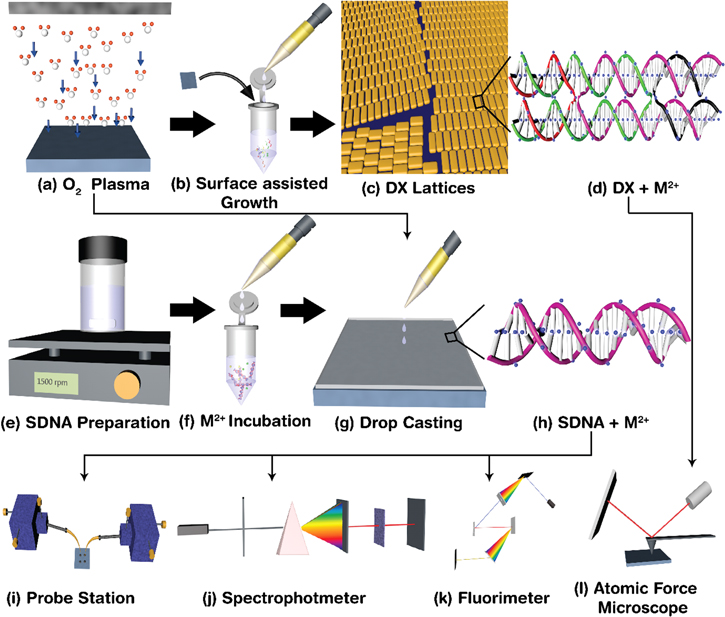
Figure 1. Schematics for the experimental procedure and physical measurements of M2+-doped DX DNA lattices and SDNA thin films: (a)–(d) preparation of M2+-doped DX DNA lattices. We treated the glass substrate by O2 plasma to render the substrate hydrophilic and to enhance the adhesion of the DNA molecules; we added individual DX DNA strands and various M2+ along with the substrate in order to grow DX DNA lattices on the substrate during the course of annealing; DX tiles doped with M2+ form lattices on the substrate; and M2+ binding sites (marked as blue dots) on a DX tile; (e)–(h) SDNA preparation by magnetic stirring; incubation with M2+ for doping; fabrication of an M2+-doped SDNA thin film by drop-casting on the O2 plasma treated glass substrate; and M2+ binding sites on a SDNA duplex; (i)–(l) cartoon representations of probe station, spectrophotometer, fluorimeter, and AFM for physical measurements—current, absorption, PL, and phase, respectively—of M2+-doped SDNA thin films and DX DNA lattices.
Download figure:
Standard image High-resolution image2.2. Preparation of the M2+-doped SDNA thin films by the drop-casting method
A solution of SDNA (GEN Corporation, Shiga, Japan) was prepared by dissolving 0.1 g of SDNA in 10 ml of deionized water and was kept overnight with magnetic stirring to achieve a homogeneous mixture of SDNA (achieving 1 wt% of SDNA). Aliquots of SDNA solution (100 μl) were pipetted into a new test-tube along with 100 μl of proper concentrations of M2+ solution. The resulting solution was vortexed for 5 min, then incubated for 24 h at room temperature, after which double and triple M2+-doped SDNA solutions (with a 0.5 wt% final concentration of SDNA) were obtained. A thin film of M2+-doped SDNA solution was fabricated by drop-casting 20 μl of the sample solution on an O2 plasma-treated substrate, with a thickness ∼1.5 μm (second row in figure 1).
2.3. AFM imaging
The morphological stability of M2+-doped DX DNA lattices grown on glass was studied by AFM imaging. The M2+-doped DX DNA sample substrate was fixed on a metal puck using instant glue and 30 μl of 1× TAE/Mg2+ buffer was pipetted onto the substrate, while another 20 μl of 1× TAE/Mg2+ was dispensed on a silicon nitride AFM tip (NP-S10, Veeco Inc., NY, USA). The AFM images were obtained by using a Multimode Nanoscope III (Veeco Inc., NY, USA) in fluid tapping mode. (Figures 2 and S2 is available online at stacks.iop.org/NANO/28/405702/mmedia in the online supplementary data (OSD).)
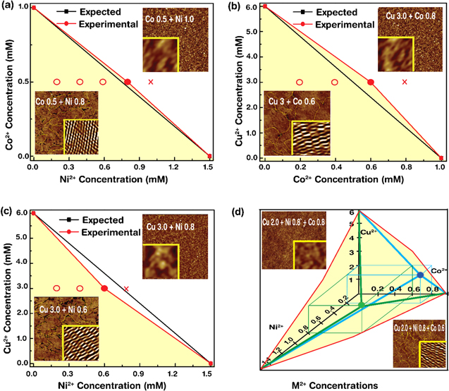
Figure 2. Phase diagrams and representative AFM images of double and triple M2+-doped DX DNA lattices. Double M2+-doped DX DNA lattices with the 3 combinations of M2+: (a) Co2+ 0.5 mM fixed and Ni2+ varied from 0.2 to 1.0 mM by increments of 0.2 mM marked with either a circle (crystalline phase) or a cross (amorphous). Phase transition occurred from crystalline (up to 0.8 mM ≡ [Ni2+]O, the optimum concentration of Ni2+ at a given condition) to amorphous (at 1.0 mM of [Ni2+]). For simplicity, we marked the region of crystalline phase as light yellow; (b) Cu2+ 3.0 mM fixed and Co2+ varied. We observed phase transition between 0.6 mM (≡[Co2+]O) and 0.8 mM of [Co2+]; (c) Cu2+3.0 mM fixed and Ni2+ varied. Phase transition occurred between 0.6 mM (≡[Ni2+]O) and 0.8 mM of [Ni2+]. We obtained an expected phase slope by the following condition, ![$\tfrac{[{{\rm{M}}}_{1}^{2+}]}{{[{{\rm{M}}}_{1}^{2+}]}_{{\rm{O}},{\rm{S}}}}+\tfrac{[{{\rm{M}}}_{2}^{2+}]}{{[{{\rm{M}}}_{2}^{2+}]}_{{\rm{O}},{\rm{S}}}}=1,$](https://content.cld.iop.org/journals/0957-4484/28/40/405702/revision2/nanoaa879bieqn2.gif) where
where  and
and  were two different types of M2+, and
 ![${[{{\rm{M}}}_{1}^{2+}]}_{{\rm{O}},{\rm{S}}}$](https://content.cld.iop.org/journals/0957-4484/28/40/405702/revision2/nanoaa879bieqn5.gif)
![$({[{{\rm{M}}}_{2}^{2+}]}_{{\rm{O}},{\rm{S}}})$](https://content.cld.iop.org/journals/0957-4484/28/40/405702/revision2/nanoaa879bieqn6.gif) was the optimum concentration of
was the optimum concentration of 
 estimated from single
  -doped DX DNA lattices; (d) Triple M2+-doped DX DNA lattices of M2+. First, Cu2+ 2.0 mM and Ni2+ 0.8 mM fixed and Co2+ varied from 0.2 mM to 0.8 mM by increments of 0.2 mM (green lines). The phase transition from crystalline to amorphous occurred between 0.6 mM (≡[Co2+]O) and 0.8 mM of [Co2+]). We placed a green dot on the yellow shaded surface, (i.e., a phase boundary). Second, Cu2+ 2.0 mM and Ni2+ 0.2 mM fixed and Co2+ varied from 0.2 mM to 1.0 mM (blue). We obtained phase transition between 0.8 mM (≡[Co2+]O) and 1.0 mM of [Co2+]. We placed a blue dot on the yellow shaded surface. In AFM images (scan size 1 μm × 1 μm), yellow dotted lines in the crystalline phase indicate M2+-doped DX DNA lattice boundaries and insets (scan size 100 nm × 100 nm) contain noise-filtered reconstructed images by fast Fourier-transformation. In the amorphous phase, no periodic DX DNA tiles were visible.
Download figure:
Standard image High-resolution image2.4. Current–voltage (I–V) measurement
Silver contacts were deposited as electrodes (channel gap distance of ∼1 mm) on the glass substrate having an M2+-doped SDNA thin film. I as the function of applied V was measured within a range between −3.0 and 3.0 V, using a probe station with two terminals (4200–SCS, Keithley Instruments Inc., OH, USA) under atmospheric pressure and room temperature. (Figure 3).

Figure 3. Current–voltage (I–V) characteristics of double and triple M2+-doped SDNA thin films. I–V of SDNA without M2+ and with various combinations of [M2+]. Double M2+-doped SDNA thin films: (a) Co2+ 0.5 mM fixed (labeled as Co 0.5), Ni2+ varied from 0.2, 0.4, 0.6, 0.8, and 1.0 mM (labeled as Ni 0.2, Ni 0.4, Ni 0.6, Ni 0.8, and Ni 1.0, respectively); (b) Cu2+ 3.0 mM fixed (Cu 3.0), Co2+ varied from 0.2, 0.4, 0.6, 0.8, and 1.0 mM (Co 0.2, Co 0.4, Co 0.6, Co 0.8, and Co 1.0, respectively); (c) Cu2+ 3.0 mM fixed (Cu 3.0), Ni2+ varied from 0.2, 0.4, 0.6, 0.8, and 1.0 mM (Ni 0.2, Ni 0.4, Ni 0.6, Ni 0.8, and Ni 1.0, respectively). Triple M2+-doped SDNA thin films: (d) Cu2+ 2.0 and Ni2+ 0.2 mM fixed (Cu 2.0 and Ni 0.2), Co2+ varied from 0.2, 0.4, 0.6, 0.8, and 1.0 mM (Co 0.2, Co 0.4, Co 0.6, Co 0.8, and Co 1.0, respectively); (e) Cu2+ 2.0 and Ni2+ 0.8 mM fixed (Cu 2.0 and Ni 0.8), Co2+ varied from 0.2, 0.4, 0.6, 0.8, and 1.0 mM (Co 0.2, Co 0.4, Co 0.6, Co 0.8, and Co 1.0, respectively). (f) Resistance as a function of varying [M2+] at a fixed V, 3 V in each of double and triple M2+-doped combinations of SDNA thin films.
Download figure:
Standard image High-resolution image2.5. Ultraviolet–visible (UV–vis.) spectroscopy measurement
The optical absorbance of SDNA thin films (on fused silica in the visible and ultraviolet regions) was measured without and with various [M2+] by a spectrophotometer (Cary 5G, Varian, CA, USA). The spectrophotometer was equipped with two light sources (a deuterium arc lamp for near-infrared and Vis., and a quartz W–halogen lamp for UV) and two detectors (a cooled PbS detector for the near-infrared region, and a photomultiplier tube for the Vis. and UV regions) (figure 4).

Figure 4. Absorbance of double and triple M2+-doped SDNA thin films. Double M2+-doped SDNA thin films: (a) Co2+ 0.5 mM fixed, Ni2+ varied from 0.2, 0.4, 0.6, and 0.8 mM; (b) Cu2+ 3.0 mM fixed, Co2+ varied from 0.2, 0.4, 0.8, and 1.0 mM; (c) Cu2+ 3.0 mM fixed, Ni2+ varied from 0.2, 0.6, 0.8, and 1.0 mM. Triple M2+-doped SDNA thin films: (d) Cu2+ 2.0 and Ni2+ 0.2 mM fixed, Co2+ varied from 0.2, 0.4, 0.6, and 0.8 mM; and (e) Cu2+ 2.0 and Ni2+ 0.8 mM fixed, Co2+ varied from 0.2, 0.4, 0.6, and 0.8 mM. (f) Absorbance peak intensities with respect to varying [M2+] at a fixed wavelength of 260 nm obtained from (a)–(e).
Download figure:
Standard image High-resolution image2.6. PL measurement
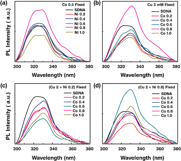
The PL emission and excitation spectra of SDNA thin films were collected without and with various [M2+] on fused silica by using a fluorimeter (FS-2, Scinco, Seoul, Korea), equipped with the Xe-arc lamp at a power of 25 W and room temperature. The emission spectra were acquired by exciting an M2+-doped SDNA thin film at a wavelength of 290 nm, and the excitation spectrum was obtained at a fixed emission wavelength, 330 nm (figures 5, S3 in OSD).
Figure 5. Photoluminescence emission spectra of SDNA thin films without M2+ and with various combinations of [M2+] at an excitation wavelength of 290 nm. Double M2+-doped SDNA thin films: (a) Co2+ 0.5 mM fixed, Ni2+ varied from 0.2, 0.4, 0.6, 0.8, and 1.0 mM; (b) Cu2+ 3.0 mM fixed, Co2+ varied from 0.2, 0.4, 0.6, 0.8, and 1.0 mM. Triple M2+-doped SDNA thin films: (c) Cu2+ 2.0 and Ni2+ 0.2 mM fixed, Co2+ varied from 0.2, 0.4, 0.6, 0.8, and 1.0 mM; and (d) Cu2+ 2.0 and Ni2+ 0.8 mM fixed, Co2+ varied from 0.2, 0.4, 0.6, 0.8, and 1.0 mM.
Download figure:
Standard image High-resolution image
3. Results and discussion
Doping of DX DNA lattices (a representative synthetic DNA nanostructure with relatively higher production yield) and SDNA thin films (natural DNA available in large quantities at low cost) were carried out by using Cu2+, Ni2+, and Co2+ (chosen due to relatively high conductivities and distinctive optical spectra, with stable ionic states compared to the pristine DNA). A DX tile—dimension of 4 nm × 12 nm in width and length—based DNA lattice used in this study had two repeating DX tiles (DX-1 and DX-2, as shown in figure S1 and tables S1, S2 in OSD). The DX DNA lattices were grown on a given substrate by the SAG method, with details of sample preparation explained in the experimental section. During the course of annealing via SAG, DNA crystallization was achieved by a growth process (including tile seeding, nucleation, and growth), resulting in polycrystalline DX DNA lattices with 50 nM of (DX) (enough for full coverage on the substrate). In addition, we used pristine DNA derived from marine salmon for fabricating SDNA thin films via the drop-casting method. During the doping process, M2+ could be freely intercalated between a base pair and bound into the negatively charged phosphate backbones (shown in figure 1).
Previously, we constructed DX DNA lattices doped with single M2+, studying their structural stabilities in a relationship with various [M2+] [24, 25, 30]. [M2+]O,S was estimated from single M2+-doped DX DNA lattices (e.g., [Cu2+]O,S = 6.0 mM, [Ni2+]O,S = 1.5 mM, and [Co2+]O,S = 1.0 mM). Up to [M2+]O,S, the crystalline phase of the DX DNA lattices with single M2+ was guaranteed, while the amorphous phase of the lattices occurred above [M2+]O,S [24]. In this study, multiple M2+-doped DX DNA lattices were fabricated at a fixed ![$[{{\rm{M}}}_{1}^{2+}]$](https://content.cld.iop.org/journals/0957-4484/28/40/405702/revision2/nanoaa879bieqn10.gif) with a varying
with a varying ![$[{{\rm{M}}}_{2}^{2+}]$](https://content.cld.iop.org/journals/0957-4484/28/40/405702/revision2/nanoaa879bieqn11.gif) for double doping, and at fixed
for double doping, and at fixed ![$[{{\rm{M}}}_{1}^{2+}]$](https://content.cld.iop.org/journals/0957-4484/28/40/405702/revision2/nanoaa879bieqn12.gif) and
and ![$[{{\rm{M}}}_{2}^{2+}]$](https://content.cld.iop.org/journals/0957-4484/28/40/405702/revision2/nanoaa879bieqn13.gif) with a varying
with a varying ![$[{{\rm{M}}}_{3}^{2+}]$](https://content.cld.iop.org/journals/0957-4484/28/40/405702/revision2/nanoaa879bieqn14.gif) for triple. Here
for triple. Here 
 and
and  represented different species of M2+ (i.e., Cu2+, Ni2+, and Co2+). Analyzing the obtained AFM images gave
 ![${[{{\rm{M}}}_{2}^{2+}]}_{{\rm{O}}}$](https://content.cld.iop.org/journals/0957-4484/28/40/405702/revision2/nanoaa879bieqn18.gif) for double doping and
for double doping and ![${[{{\rm{M}}}_{3}^{2+}]}_{{\rm{O}}}$](https://content.cld.iop.org/journals/0957-4484/28/40/405702/revision2/nanoaa879bieqn19.gif) for triple doping, followed by the completion of the phase diagram (a graphical representation of the crystalline and amorphous phases as a function of [M2+]). DX DNA lattices with multiple M2+ dopants might have the inherent characteristics of each species of M2+ while fine-tuning the functionality of the DX DNA lattices by controlling the combinations of M2+ was possible (advantageous compared to single doping).
for triple doping, followed by the completion of the phase diagram (a graphical representation of the crystalline and amorphous phases as a function of [M2+]). DX DNA lattices with multiple M2+ dopants might have the inherent characteristics of each species of M2+ while fine-tuning the functionality of the DX DNA lattices by controlling the combinations of M2+ was possible (advantageous compared to single doping).
We could expect the crystalline domain region with multiple M2+-doped DX DNA lattices to follow a relationship between the each species of [M2+] and [M2+]O (for single M2+-doping, [M2+]O was estimated from the data of a single M2+-doped DX DNA lattice). For double  and
and  -doping, the crystalline, and amorphous phases were to meet the following conditions,
 ![$\tfrac{[{{\rm{M}}}_{1}^{2+}]}{{[{{\rm{M}}}_{1}^{2+}]}_{{\rm{O}},{\rm{S}}}}+\tfrac{[{{\rm{M}}}_{2}^{2+}]}{{[{{\rm{M}}}_{2}^{2+}]}_{{\rm{O}},{\rm{S}}}}\leqslant 1,$](https://content.cld.iop.org/journals/0957-4484/28/40/405702/revision2/nanoaa879bieqn22.gif) and
and ![$\tfrac{[{{\rm{M}}}_{1}^{2+}]}{{[{{\rm{M}}}_{1}^{2+}]}_{{\rm{O}},{\rm{S}}}}+\tfrac{[{{\rm{M}}}_{2}^{2+}]}{{[{{\rm{M}}}_{2}^{2+}]}_{{\rm{O}},{\rm{S}}}}\gt 1,$](https://content.cld.iop.org/journals/0957-4484/28/40/405702/revision2/nanoaa879bieqn23.gif) respectively. The expected lines in a phase diagram of
respectively. The expected lines in a phase diagram of  and
and  -doped DX DNA lattices as shown in figures 2(a)–(c) separated the crystalline and amorphous phases of the DX DNA lattices in 2-dimensional phase diagrams. Here, the ratio of
 ![${[{{\rm{M}}}_{2}^{2+}]}_{{\rm{O}},{\rm{S}}}$](https://content.cld.iop.org/journals/0957-4484/28/40/405702/revision2/nanoaa879bieqn26.gif) to
to ![${[{{\rm{M}}}_{1}^{2+}]}_{{\rm{O}},{\rm{S}}}$](https://content.cld.iop.org/journals/0957-4484/28/40/405702/revision2/nanoaa879bieqn27.gif) indicated the slope magnitude of the expected line. In the 3-dimensional phase diagram shown in figure 2(d), a crystalline triangular surface was defined by a condition,
indicated the slope magnitude of the expected line. In the 3-dimensional phase diagram shown in figure 2(d), a crystalline triangular surface was defined by a condition, ![$\tfrac{[{{\rm{M}}}_{1}^{2+}]}{{[{{\rm{M}}}_{1}^{2+}]}_{{\rm{O}},{\rm{S}}}}+\tfrac{[{{\rm{M}}}_{2}^{2+}]}{{[{{\rm{M}}}_{2}^{2+}]}_{{\rm{O}},{\rm{S}}}}+\tfrac{[{{\rm{M}}}_{3}^{2+}]}{{[{{\rm{M}}}_{3}^{2+}]}_{{\rm{O}},{\rm{S}}}}=1.$](https://content.cld.iop.org/journals/0957-4484/28/40/405702/revision2/nanoaa879bieqn28.gif) Even though the expected surface was not drawn for simplicity, but it is expected to be similar to the light yellow shaded region obtained by the experimental data.
Even though the expected surface was not drawn for simplicity, but it is expected to be similar to the light yellow shaded region obtained by the experimental data.
Figure 2 depicted the characteristic AFM images for double and triple M2+-doped DX DNA lattices with phase diagrams. AFM images verified the crystalline and amorphous phases controlled by different combinations of [M2+] in the DX DNA lattices. [M2+] for double-doping was used in the following combinations: (i) Co2+ 0.5 mM fixed, Ni2+ varied from 0.2 to 1.0 mM by increments of 0.2 mM, and phase transition occurred from crystalline (up to 0.8 mM ≡ [Ni2+]O) to amorphous (at 1.0 mM of [Ni2+]) (indicated by a red dot located on the red line); (ii) Cu2+ 3.0 mM fixed, and Co2+ varied from 0.2 mM to 0.8 mM, and phase transition occurred between 0.6 mM (≡[Co2+]O) and 0.8 mM of [Co2+]; and (iii) Cu2+ 3.0 mM fixed, and Ni2+ varied 0.2 to 0.8 mM, while phase transition occurred between 0.6 mM (≡[Ni2+]O) and 0.8 mM of [Ni2+]. By using the definition for percentage of discrepancy between the expected and the experimental values, calculated as (∣[M2+]O,Expected − [M2+]O,Experimental∣/[M2+]O,Expected) ×100, we obtained relatively larger percentages of discrepancy, (i) 6.7%, (ii) 20.0, and (iii) 20.0, due to small sample sets (we analyzed 3 sets of each M2+ combination). Similarly, we prepared two cases of triple doping: (i) Co2+ varied from 0.2 mM to 0.8 mM by increments of 0.2 mM, at fixed Cu2+ 2.0 mM and Ni2+ 0.8 mM, and phase transition from crystalline to amorphous occurred between 0.6 mM (≡Co2+]O) and 0.8 mM of [Co2+]) (indicated by a blue dot located on the surface of the yellow shaded region); and (ii) Co2+ varied from 0.2 mM to 1.0 mM, at a fixed Cu2+ 2.0 mM and Ni2+ 0.2 mM, where phase transition occurred between 0.8 mM (≡[Co2+]O) and 1.0 mM of [Co2+]) (indicated by a green dot placed on the surface of the yellow shaded region).
The light yellow shaded and the white regions denoted in graphs (figure 2) indicated the crystalline and amorphous domains of M2+-doped DX DNA lattices, respectively. The yellow lines in the AFM images in the crystal domain showed the M2+-doped DX DNA lattice boundaries, while the insets in those graphs contained noise-filtered reconstructed images by fast Fourier-transformation that indicated the periodicities in the DX lattices (crystalline phase). The periodicity of DX DNA lattices was not visible in the amorphous phase (confirmed by fast Fourier-transformation). Additional AFM images for M2+-doped DX DNA lattices for the rest of [M2+] are shown in figure S2 in OSD. In the presence of the excess M2+(=[M2+] –[M2+]O), deformation of DX DNA lattices occurred due to the improper and nonspecific bindings of excess M2+ into the DNA molecules [24, 25, 30, 31].
The measurements of M2+-doped SDNA thin films (∼1.5 μm of thickness) carried out for I (conductivity), UV–vis. absorption (binding of M2+ to DNA), and PL (fluorescence characteristic) showed consistent and reproducible characteristics compared to the M2+-doped DX DNA lattices (∼2.0 nm of thickness) due to the substantial sample volume at a given area. SDNA served as a readily available natural source of DNA, extracted from salmon fish and processed enzymatically to yield relatively higher amounts of pure DNA molecules. Figure 3 showed the I–V characteristics (measured by a two terminal source-drain configuration) and resistance (R, calculated from Ohm's law, R = V/I) of multiple M2+-doped SDNA thin films. I curves for multiple M2+-doped SDNA thin films were roughly linearly proportional to the applied V, majorly due to the hopping of charge carriers through the dopants in DNA duplex [32, 33]. From figure 3, we noticed that I heavily relied on the various combinations of [M2+], as well as the different types of M2+. Figure 3(f) showed a graphical representation for R against varying [M2+] of multiple M2+-doped SDNA thin films at a fixed 3 V. The minimum R values obtained, for a double doping group with varying Ni2+ (Co2+, Ni2+) from 0.2 mM to 1 mM at fixed Co2+ 0.5 mM (Cu2+ 3.0 mM, Cu2+ 3.0 mM) were 0.12 GΩ (0.75 GΩ, 0.13 GΩ) at 0.8 mM of [Ni2+] (0.6 mM of [Co2+], 0.6 mM of [Ni2+])—coincidently identical to [Ni2+]O ([Co2+]O, [Ni2+]O) obtained from phase diagrams discussed in figure 2. Similarly the minimum R obtained for a triple doping group, with varying Co2+ (Co2+) from 0.2 mM to 1.0 mM at fixed Cu2+ 2.0 mM and Ni2+ 0.2 mM (Cu2+ 2.0 mM and Ni2+ 0.8 mM) were 0.10 GΩ (0.91 GΩ) at 0.8 mM of [Co2+] (0.6 mM of [Co2+])—also identical to [Co2+]O ([Co2+]O). From these observations, we could redefine [M2+]O measured through SDNA thin films as [M2+] at which R was minimum at a fixed V. We observed that R decreased (I increased) with increasing [M2+] up to [M2+]O (due to the proper DNA site binding of M2+), while R increased (I decreased) above [M2+]O (improper binding of excess M2+ on the DNA) [24].
Figure 4 depicted the absorbance (as the function of the scanned wavelength) and relative peak intensity (as a function of varying [M2+]) of multiple M2+-doped SDNA thin films (DNA molecules were known to exhibit absorption in the range of 250–280 nm). We measured 5 sets of M2+-doped combinations on SDNA thin films, 3 for double doping (Co2+0.5 mM, Cu2+ 3.0 mM, and Cu2+ 3.0 mM fixed; while Ni2+, Co2+, and Ni2+ varied, respectively), and 2 for triple doping (Cu2+ 2.0 mM and Ni2+ 0.2 mM fixed, while Co2+ varied; and Cu2+ 2.0 mM and Ni2+ 0.8 mM fixed, while Co2+ varied). Figure 4(f) summarized the absorbance peak intensities as a function of [M2+], by analyzing absorbance peaks at 260 nm. Absorbance spectra of SDNA thin film revealed quenching of the absorbance intensity after M2+-doping, due to the binding of M2+ with DNA (which compromised the stability of the DNA duplex). Absorption intensity gradually decreased up to a certain [M2+]O,ABS {for a double doping group, minimum peak intensity obtained with varying Ni2+ (Co2+, Ni2+) at fixed Co2+ 0.5 mM (Cu2+ 3.0 mM, Cu2+ 3.0 mM) at 0.4 mM of [Ni2+] (0.8 mM of [Co2+], 0.8 mM of [Ni2+]); similarly for a triple doping group, minimum peak intensity obtained with varying Co2+ (Co2+) at fixed Cu2+ 2.0 mM and Ni2+ 0.2 mM (Cu2+ 2.0 mM and Ni2+ 0.8 mM) at 0.4 mM of [Co2+] (0.4 mM of [Co2+])}, and increased above [M2+]O,ABS. Despite slight differences between [M2+]O,ABS and [M2+]O (measured from AFM and I–V), overall trends followed as expected.
The typical excitation spectra monitored at a fixed emission wavelength, 330 nm for pristine SDNA and M2+-doped SDNA thin films (data not shown) revealed a strong peak at ∼290 nm. The emission spectra for SDNA thin films without M2+ and with various combinations of [M2+] were collected at an excitation wavelength of 290 nm. PL involved the proper excitation energy to excite an electron to a singlet excited state from the singlet ground state upon absorbing the photon energy. A desirable root for relaxation was an internal conversion in which relaxation from a higher vibrational energy level of an excited state occurred toward the zero level of that excited state by the non-radiative energy transfer. The inter-system crossing was a type of non-radiative energy transfer that occurred when an electron relaxed to the triplet excited state from the singlet excited state. PL could be observed from the release of a photon upon relaxation of the electron from the triplet excited state. Thus, energy transfer occurred through an internal conversion process within the excited singlet state, then from the excited singlet state to the triplet state through the inter-system crossing, and finally to emissive states [25].
Figure 5 showed the PL emission spectra of double and triple doped M2+-doped SDNA thin films (Co2+ fixed and Ni2+ varied, Cu2+ fixed and Co2+ varied, and Cu2+ fixed and Ni2+ varied, respectively for double doping; Cu2+, Ni2+ fixed and Co2+ varied for triple). The PL spectra for M2+-doped SDNA thin films, as well as for pristine SDNA thin film, showed the peak centered at ∼330 nm, while we observed enhancing and quenching of PL intensities by controlling [M2+]. PL intensities were enhanced at Co2+ 0.5 mM with Ni2+ 0.8 mM followed by quenching with increasing [Ni2+] (figure 5(a)), and Cu2+ 3 mM with Co2+ 0.8 mM followed by quenching with increasing [Co2+] (figure 5(b)) for double doping; and Cu2+ 2 mM and Ni2+ 0.2 mM with Co2+ 1 mM (figure 5(c)), and Cu2+ 2 mM and Ni2+ 0.8 mM with Co2+ 0.6 mM (figure 5(d)) for triple, followed by quenching with increasing [Co2+]. Based on the PL graphs shown in figure 5, we expected the energy transfer from the excited states of the SDNA to the emissive states of the bound M2+ to take place from the lowest triplet excited state in M2+-doped SDNA thin films up to [M2+]O at a given condition. Above [M2+]O, the energy transfer might occur from M2+ to the SDNA through cross relaxation due to the excess M2+ bound non-specifically to SDNA molecules. Consequently, the energy transfer results revealed the PL quenching of M2+-doped SDNA thin films.
4. Conclusions
We developed a simple method to dope various M2+ to synthetic DNA lattices which provided multifunctional physical characteristics in an M2+-doped DNA thin film. We (i) fabricated synthetic DX DNA lattices and natural SDNA thin films doped with combinations of double and triple M2+-doped groups at various [M2+]; (ii) evaluated the optimum [M2+] at which phase of M2+-doped DX DNA lattices changed from crystalline to amorphous; and lastly, (iii) studied the optoelectric characteristics of multiple M2+-doped SDNA thin films. We analyzed a phase diagram by the theoretical estimation of the [M2+], confirmed experimentally by AFM. In addition, the measurement of current, absorption, and PL lead to gain an understanding concerning conductivity, chemical binding, and fluorescence. We realized that the current and PL intensities were observed maximum but the absorbance intensities showed minimum at around [M2+]O for double and triple M2+-doped SDNA thin films. Consequently, multiple M2+-doped DNA thin films may be used in physical devices and chemical sensors with tunable multiple functionalities in the near future.
Acknowledgments
This work was supported by the Center for Advanced Meta-Materials (CAMM) as Global Frontier Project (CAMM-2014M3A6B3063707, CAMM-2015M3A6B3071411) and by the National Research Foundation (NRF) of Korea (2016R1D1A1B03933768, 2017R1A2B4010955, 2017R1D1A1B03035053) funded by the Ministry of Science, ICT and Future Planning of the Korean government.