

Abstract
A new method for accurately characterizing the tip geometry of critical dimension atomic force microscopy (CD-AFM) has been introduced. A sample type IVPS100-PTB whose line features have vertical sidewall, round corner with a radius of approx. 5 ∼ 6 nm and very low surface roughness has been applied as the tip characterizer. The geometry of the line features has been accurately and traceably calibrated to the lattice constant of crystal silicon. In this paper, detailed measurement strategies and data evaluation algorithms have been introduced, particularly concerning several important influence factors such as the line width roughness of the tip characterizer, measurement noise, measurement point density, and the calculation of the averaged tip geometry. Thorough experimental studies have been carried out, indicating high measurement accuracy of the developed method. For instance, tip geometry of a probe type CDR120 with a nominal tip diameter of 120 nm is reconstructed using two different tip characterizers before, during and after it is applied for a calibration of a user sample. The agreement of all 20 obtained tip profiles reaches 0.4 nm, confirming the high measurement stability, low tip wear as well as the high measurement consistency between two tip characterizers. Furthermore, the results of a nanofeature of the user sample after correcting the tip contribution show a repeatability of approximately 0.3 nm when it is repeatedly measured by a same tip, and a reproducibility of 0.9 nm when it is measured using two different tips, confirming the good performance of the tip correction method as well.
Export citation and abstract BibTeX RIS

Original content from this work may be used under the terms of the Creative Commons Attribution 4.0 license. Any further distribution of this work must maintain attribution to the author(s) and the title of the work, journal citation and DOI.
1. Introduction
Atomic force microscopy (AFM) has rapidly become a popular microscopic technique for characterizing, measuring, and manipulating various nanostructures since its invention in the year 1986 [1]. A fundamental concern in AFM measurements is the AFM tip. The tip-sample interaction represents the most critical properties of AFM measurements. For instance, the tip geometry directly impacts the tip-sample interaction force and defines the resolution capability. From the morphological point of view, the profile measured by an AFM is the dilated result of the real structure by the so-called effective tip geometry [2, 3]. Here, the effective tip geometry takes both, the physical tip geometry and the tip sample interaction, into account [3]. To derive the real geometry of measured structures, the effective geometry of the applied tip must be reconstructed accurately, and then its contribution in measured AFM images should be corrected.
3D nanometrology of complex nanostructures are a challenging task for e.g. the next generation of semiconductor devices [4]. Two types of AFM are mainly applied today for measuring 3D shape of nanofeatures. One type is called as tilting-tip AFM method [5, 6]. In a tilting-tip AFM, complex features are measured with an AFM tip tilted at different angles up to ±40° off the normal; the data of obtained images will be fused together to derive the 3D feature geometry. The other type is usually referred to as critical dimension atomic force microscopy (CD-AFM) [7]. It utilizes a kind of flared AFM tip which has an extended feature near the tip end, thus allowing the probing of vertical or even undercut features directly. Both types of AFMs have advantages and disadvantages. The tilting-tip AFM has advantage that tips with a simple conical or pyramidal tip shape can be applied. However, multiple measurements need to be performed at different tip-titled angles, and the uncertainty in aligning and fusing measurement data sets may directly impact the measurement uncertainty. In contrast, the CD-AFM is capable of obtaining the 3D shape of nanofeatures in a single image. However, the flared tip shape applied in CD-AFM has more complex geometry, posing a significant challenge in tip characterization.
Different characterization methods of AFM tip geometry are available today, for instance direct imaging method [8], tip-on-tip imaging method [9], and tip reconstruction method [2, 3, 10–14]. The direct imaging method applies high resolution microscopes to get a visual image which directly represents the AFM tip geometry. Secondary electrons (SE) image in a scanning electron microscope (SEM) is often used for imaging AFM tips. It has a capable lateral resolution down to about 1 nm. However, it has several drawbacks. Firstly, the measurement cannot be performed in situ. AFM tips must be mounted and dismounted for measurements in AFM and SEM instruments, which is very time consuming. Secondly, SEM measurements may suffer from the known charging and contamination issues. The charging issue may distort and/or blur the measured SEM image, particularly when AFM tips are measured at high magnifications. Contamination effects may alter or even damage the measured tips, consequently, a trade-off between the SEM exposure time and the imaging noise must be taken. Furthermore, the tip-sample interaction of AFM measurement is not concerned when the tip geometry is measured by a SEM, consequently the result may slightly differ from the effective tip geometry.
The tip-on-tip imaging method has been recently proposed by NIST [9] for calibrating the tip width using the error separation technique, analogue to the method applied for calibrating the probe geometry of a micro coordinate measuring machine [15]. Using this method, three CD-AFM tips (denoted as A, B, and C) with unknown tip widths (denoted as dA, dB, dc) measure against each other, resulting in three different AFM images (A–B, B–C and C–A). The apparent structure widths (WAB, WBC and WCA) of the obtained AFM images reveal the information of dA + dB, dB + dC and dC + dA, respectively. By solving three equations, three unknown tip widths can be obtained, for instance dA = (WAB + WCA − WBC)/2. This method thus allows a unique solution for accurate calibration of tip width. They achieved a combined expanded uncertainty U (k = 2) of about 1 nm for the tip type CDR120 (nominal tip width of 120 nm, Team Nanotec), and of approximately 3 nm for the tip type CDR50 (nominal tip width of 50 nm, Team Nanotec). However, the method is currently not yet applicable for calibrating the tip geometry. In addition, it is not a trial task to align an AFM tip on the top of another AFM tip for measurements, particularly when the AFM tip is very tiny.
The tip reconstruction method is based on the morphology theory underlying the AFM measurements―when nanostructures with known geometry are measured by an AFM tip, the tip geometry can be reconstructed by eroding the obtained AFM images by the known geometry of nanostructures [2, 3, 10–14]. Such nanostructures applied for reconstructing tip geometries are usually called as tip characterizers. In practice, nanostructures having very sharp but unknown (i.e. blind) geometry are often applied as tip characterizers. In the data evaluation, however, the geometry of such characterizers is usually assumed as infinitively sharp. This simplified method is called as 'Blind tip reconstruction (BTR)' method [11]. Although the tip reconstruction method has advantages of easy-of-use and is capable of determining tip geometry in situ, it has several limitations, too. Firstly, due to the lack of accurate knowledge of the real geometry of the applied tip characterizers, the uncertainty of the reconstructed tip geometry is usually high (a few nm or higher). Particularly, the BTR method reveals an upper boundary of the tip geometry only, as no tip characterizer is infinitively sharp in reality. Secondly, the method is very sensitive to measurement noises in praxis, strongly impacting the achievable measurement performance [16].
In this paper, a new tip characterizer was introduced for accurate characterization of CD-AFM tips based on the tip reconstruction method. Detailed method and algorithms are presented. Thorough experimental investigations have been carried out, indicating high achievable measurement accuracy.
2. Method
A schematic diagram showing the dilation effect of a flared CD-AFM tip in two measurement scenarios is illustrated in figure 1. In a simple measurement scenario where the structures have vertical sidewalls as shown in figure 1(a), the contribution of the tip is usually treated as a zero-order offset [17] in CD metrology, where the feature width is calculated as the apparent feature width (CDm) minus the tip width (dtip). However, if structures to be measured have more complicated 3D shape, for instance features with non-vertical sidewalls as shown in figure 1(b), accurate geometry of the applied CDR tip is required to correct the tip contribution. For the structures without undercuts, the geometry of lower part of the CDR tip as marked in red is required.

Figure 1. Schematic diagram showing the dilation effect of a CDR tip in two measurement scenarios: (a) in a measurement scenario of structures with vertical sidewalls, the contribution of the tip can be corrected by subtracting the apparent structure width (CDm) by the tip width (dtip) as a zero-order offset; (b) in measurements of nanostructures with non-vertical sidewalls, the tip form must be corrected using morphological operations with the known effective tip geometry.
Download figure:
Standard image High-resolution imageThe tip characterization method we applied in this study belongs to the tip reconstruction method based on the morphological mathematics. In an AFM measurement, the obtained AFM image (I) can be interpreted as the dilated result of real structure (S) by the applied tip geometry (T):

where  denotes the morphological operation of dilation.
The tip geometry T can be reconstructed from the AFM image (I) by using the known structure geometry (S) by the morphological operation of erosion:

where  denotes the morphological operation of erosion.
After the tip geometry (T) is reconstructed, it can be applied to correct the AFM image (I) to obtain the corrected geometry of structures (S) being measured:

The physical meaning of equations (2) and (3) is actually similar. It represents that an AFM measurement can be interpreted in two different perspectives, either as the result when the structure S probed by the tip T, or as the result when the tip T (acting as a 'sample') probed by the structure S (acting as a 'tip').
Although the tip reconstruction method based on the morphological mathematics is rather straight forward, it remains as a big challenge today to achieve sub-nm accuracy. The main reasons are owing to two aspects. The first aspect concerns the challenge to obtain a tip characterizer whose geometry is accurately known. As one can easily understand from equation (2), the uncertainty of S will be directly propagated to the uncertainty of T. To reconstruct the tip geometry with sub-nm accuracy, S is needed to be known with sub-nm accuracy, too. The second aspect concerns the careful optimization of the algorithm to reduce the influences such as measurement noise.
To solve the first problem as mentioned above, we applied a line width standard type IVPS100-PTB jointly developed by the PTB and the company Team Nanotec [18]. The IVPS100-PTB sample has a size of 6 mm × 6 mm, consisting of 4 groups of 5 × 5 feature patterns. Each feature pattern has a group of five reference line features with a nominal CD of 50 nm, 70 nm, 90 nm, 110 nm and 130 nm, respectively. The line feature has almost vertical sidewall, round corner with a radius of approx. 5 ∼ 6 nm, and very low surface roughness [18]. A key advantage of applying this type of standard lies that the geometry of its line features can be well determined using a new traceability approach referred to as a 'bottom-up approach' [19, 20]. The concept of the bottom-up approach is to apply the crystal lattice as an internal ruler for accurately and traceably determining the geometry of nanostructures made of crystal materials such as silicon. To realize the bottom-up approach, a cross-sectional slice of the structure to be measured (usually called as a lamella) needs to be prepared, usually by a focus ion beam (FIB) tool. Then the lamella can be measured by the state-of-the-art spherical aberration corrected high-resolution transmission electron microscopy (HR-TEM), which is capable of microscopic imaging and microanalysis with a spatial resolution down to 0.05 nm, i.e. true atomic resolution. Figure 2 illustrates the determined geometry of a line feature of an IVPS100-PTB sample obtained in our previous study [18].
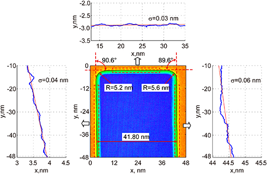
Figure 2. Geometry of an IVPS100-PTB line feature accurately determined by the state-of-the-art (S)TEMs technique using the crystal lattice constant of silicon as an internal 'ruler' [18].
Download figure:
Standard image High-resolution imageA remaining problem in applying the bottom up traceability route mentioned above is the so-called dissemination issue. As the sample needs to be destructively prepared for TEM measurements, it is no more available for tip characterization. To solve this problem, a strategy for non-destructive calibration is suggested [18]. The strategy consists of three steps. In the first step, two groups of specimens are selected, one as the reference structures and the other as the TEM target structures. The two groups of specimens are measured by a CD-AFM using a same flared tip under the same measurement conditions. Their results are registered. In the second step, the TEM target structures are measured destructively and their dimension can be evaluated. In the third step, the (effective) tip geometry can be evaluated based on the TEM reference values. With the known (effective) tip geometry, the dimension of the reference structures can be calculated, too. Although the reference structures were not measured by TEM, they can be well applied for reference metrology.
Further study has shown that different line features of IVPS100-PTB samples have similar corner radii. Figure 3 plots determined corner radii of line features of three different IVPS100-PTB samples. It can be seen that the corner radii of different line features and over different samples are quite consistent. The mean value of the corner radii is 5.8 nm and its standard deviation is about 0.4 nm. We expect that the variation of the corner radii has a stochastic behavior which is related with the lithography and etching processes. Thus its contribution to the uncertainty of tip reconstruction can be further reduced by averaging results obtained from multiple feature lines, as will be detailed in section 3.2.
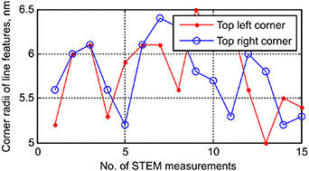
Figure 3. Determined corner radii from STEM images using the crystal lattice constant of silicon as an internal ruler. The obtained results from 15 STEM measurements on different line features show similar corner radii of different line features. The mean value of the measured corner radii is 5.8 nm and its standard deviation of 15 measurements is about 0.4 nm.
Download figure:
Standard image High-resolution imageThe imaging processing of an IVPS100-PTB line feature by a CD-AFM flared tip is illustrated in figure 4(a). For better understanding, the tip form drawn in the figure is divided to 6 parts, i.e. the leftmost light blue point, the rightmost green point, the lowest red point, the purple curve between the light blue point and red point, the dark blue curve between the green point and red point, and the upper orange part. For every scanning step, the reference structure contacts with a point of the tip. For the three horizontal parts '1' of the reference structure, the contact point is the lowest red point of the tip, and it exactly contributes for the imaging points, which are also colored red. For the left sidewall part '2' of the reference structure, the contact point is the rightmost green point of the tip, and the position of the tip apex contributes for the image points, which are colored green. For the left rounding corner part '3' of the reference structure, the contact point walks along the dark blue curve of the tip, and the position of the tip apex contributes for the image points, which are colored dark blue. The similar process for the right rounding corner and the right sidewall of the reference structure. Every image point is rendered to illustrate that it contains the information of a tip point with the same color. Therefore, the information of the tip form reconstruction most relies on the parts '2', '3', '4' '5' of the reference structure, where the parts '2' and '5' determines the tip width while the parts '3' and '4' reveal the tip form. For obtaining a more detailed information about the tip form, the parts '3' and '4' need to be measured with high point density. In addition, the upper orange part of the tip from does not contribute in measurements, consequently, it is not able to be reconstructed using this tip characterizer. However, this part of tip form is only interested if structures with undercuts are to be measured, which is not the focus of our study. Alternatively, a similar kind of tip characterizer type IFSR (Team Nanotec) can be applied using a similar method proposed in this paper.

Figure 4. (a) Schematic diagram showing the imaging of the IVPS line structure by a CDR tip; (b) a measured CD-AFM image of a group of 5 line features with nominal widths of 50 nm, 70 nm, 90 nm, 110 nm and 130 nm showing as raw data.
Download figure:
Standard image High-resolution imageAs an example, figure 4(b) demonstrate a CD-AFM image taken on a group of line features of an IVPS100-PTB sample, shown as raw data. The measurement is performed by a CD-AFM developed at PTB [21]. A key feature of the CD-AFM is that it applies a so-called vector approaching probing (VAP) strategy in measurements [21]. Using the VAP strategy, the feature surface is probed by a CD-AFM tip in a direction quasi orthogonal to the feature surface point by point. It offers advantages such as better 3D probing sensitivity, lower tip wear and more flexibility in defining desired measurement points. In the measurement example shown in figure 4(b), the top left and top right corners of the line features are measured with 20 points each, thus offer good point density for reconstructing the tip form. In addition, the base line of profiles of measured image show a slight tilting angle of about 1.1°, which is attributed to the inclination of the sample when it is mounted in the AFM tool. It is corrected by rotating the measurement data by a rotation matrix defined by the determined tilting angle.
A tip form reconstruction process is illustrated in figure 5. The data set S indicates the applied line structure after rotated by 180°, thus the line feature indicated by S becomes downwards. At the beginning of reconstruction process, the apex of S is coincided with the first point of the dataset of the image profile, shown as I. From here, S starts to 'walk' following every point of I, and dataset I is reduced by the intersection with S step by step. Parts of the dataset S are plotted as blue lines in figure 5 to show the erosion process for the sake of brevity and readability. By completing this erosion process, the obtained boundary contour of the eroded dataset I shown as the orange dashed line represents the reconstructed tip form. However, it should be stressed that only the upper part of the curve reveals the tip form, as illustrated in figure 5. The reason has been explained in figure 4(a), that the upper part of the tip cannot be reconstructed because it has not contributed in the imaging process of the sample.
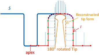
Figure 5. Schematic diagram showing the basic principle of tip reconstruction.
Download figure:
Standard image High-resolution imageTo apply the method mentioned above for accurate tip reconstruction, accurate geometry of line structure at local positions where every AFM profile is taken needs to be known. There is, however, a problem in practice, as the width of IVPS100-PTB line features determined by the bottom-up approach is usually an averaged value over a defined range (typically 1 ∼ 2 µm) [22]. Due to the presence of the so-called line width roughness (LWR), the width of line features at local positions could significantly deviates from the averaged value. Thus it is necessary to transfer the averaged width value to the feature width at local positions. For solving this problem we apply a multi-step approach. The first step is the determination of the effective tip width. As already illustrated in figure 1(a), the effective tip width (tw) can be simply treated as a zero-order offset as the IVPS100-PTB sample has almost vertical sidewall. In praxis, it can be simply calculated as the averaged apparent feature width calculated from measured AFM image minus the calibrated feature width. In the second step, the feature width at local positions is calculated as the apparent line width evaluated at each AFM profile minus the tip width tw. With known feature width and corner rounding radii, the geometry of line feature at local position can be generated. It can then be applied to erode the corresponding AFM profile for reconstructing the tip geometry as already illustrated in figure 5.
It should be mentioned that the characterized tip form in this study is the effective tip geometry. It differs than the physical tip geometry which is obtainable by e.g. high resolution microscopes. The effective tip geometry includes the contribution of tip-sample interactions, for instance, the tip deformation due to the tip sample interaction forces. As such tip deformation happens when the tip is calibrated and when it is applied for measurements of user samples, the correction of the 'effective' tip geometry in user measurements compensates the influence of tip deformation as well. In addition, the measurement conditions for instance the tip oscillation frequencies, oscillation amplitude and the tip alignment to samples will also impact the effective tip form. Therefore, in our study these measurement conditions of the tip are kept constant.
3. Important aspects for optimizing tip reconstruction and tip correction algorithm
Apply the method introduced above, tip geometry can be reconstructed from AFM image obtained on the tip characterizer IVPS100-PTB. In practice, however, several important aspects still need to be handled properly for obtaining accurate results. In this section, these aspects including the influence of measurement noise, the averaging of reconstructed tip geometry and the point density are detailed.
3.1. The influence of measurement noise
A practical issue in tip reconstruction is the remarkable influence owing to the measurement noise [16]. As illustrated in figure 5, the reconstructed tip from is the boundary contour of the data set when the measured data set I (representing the AFM profile) eroded by the data set S (representing the geometry of the tip characterizer) when S shifts over measurement points. Unlike the calculation of averaged value of a signal where the noise of signal can be significantly reduced, the calculation of the boundary value of a signal will be biased by the amplitude of the noise. Consequently, the reconstructed tip geometry will be significantly biased by the measurement noise.
To overcome this problem, we apply the spline filtering technique for removing the noise contribution. Figure 6 shows an example concerning this idea. Figure 6(a) depicts the measured and filtered profiles, as well as the reconstructed tip geometry from them in red (unfiltered) and blue (filtered), respectively. At first sight, the unfiltered and filtered data overlap very well, because our CD-AFM has very low measurement noise (a standard deviation of 0.13 nm in repeated point probing). However, when the data is zoomed-in at the marked box and detailed in figure 6(b), it can be clearly seen that the tip geometry is underestimated by about 0.45 nm due to the extreme noise points in the raw AFM profile marked as 'A' and 'B'. If both sides of the tip form are considered, it will lead to an underestimation of the tip size of 0.9 nm, thus introducing a significant measurement bias.
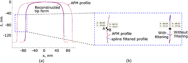
Figure 6. Influence of measurement noise on reconstruction of tip form, shown as (a) an overview of a measured AFM profile and reconstructed tip form; (b) a detailed view of the profiles in the marked area in (a). The AFM profile in red presents the raw data (after tilting correction), and its spline filtered profile is shown in blue. Due to the impacts of extreme points such as points marked as 'A' and 'B', the tip form will be underestimated if no filtering is applied.
Download figure:
Standard image High-resolution imageThe order of the spline filtering is selected in such a way that the filtered AFM profile becomes smooth while its form is well kept. Our developed software offers a graphic user interface for conveniently setting a filtering order, as well as testing its filtering behaviour.
Other techniques such as Gaussian filter or morphological filter, which are widely applied for roughness parameter evaluation in stylus instruments, could also be suitable for reducing the measurement noise. These filtering techniques are worthy of being studied and compared.
3.2. Calculation of averaged tip geometry
In a tip reconstruction measurement as shown in figure 4(b), 5 line features are measured with 8 profiles. After tip reconstruction, totally 5 × 8 tip profiles will be obtained. These tip profiles need to be averaged to obtain an averaged tip geometry. This averaging process is also beneficial to reduce the influence of the corner radii variation of the applied line features of the tip characterizer.
Figure 7 shows an example illustrating how the mean tip profile is calculated. From the reconstructed point clouds of all 40 tip profiles, the points are first grouped in many segments as shown in figure 7(a) and detailed in figure 7(b). Center points of each data group as marked in green is then calculated as mean tip profile. In addition, the standard deviation σ of each data group indicates the precision of the tip reconstruction can be also obtained at each point. In the given example, a standard deviation σ is about 0.5 nm, indicating the high measurement precision of the applied method. According to the 'guide to the expression of uncertainty in measurement (GUM)' [23], the variance of the averaged tip profile from 40 independent observations can be theoretically reduced to  .
.
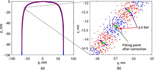
Figure 7. Calculation of the averaged tip geometry from 40 individual tip profiles, shown as (a) reconstructed data points of individual tip profiles are grouped; and (b) a zoomed-in view of tree groups of data points. Center points of each data group as marked in green are calculated as mean tip profile. The standard deviation  of each data group indicates the precision of the tip reconstruction at that point.
Download figure:
Standard image High-resolution image3.3. Influence of measurement point density
Sample surface is presented as discrete points in AFM measurements. Consequently, the point density will also influence the accuracy of tip reconstruction and tip correction. As an example, figure 8(a) illustrates the tip correction process, where an AFM profile obtained on a user sample is eroded with the reconstructed tip geometry. This process is similar to that shown in figure 5, except the data set of the reconstructed tip (T) is applied instead. For clarity, part of the data in the marked box is zoomed-in in figure 8(b). The raw data points, tip profile (T) and reconstructed surface are clearly illustrated. It can be seen that due to the limited point density of the measured AFM profile, the tip corrected result appears a kind of wave artefact.

Figure 8. The process of correcting tip contribution in measurement of a user sample with the reconstructed tip geometry, shown as (a) the reconstructed tip geometry erodes an AFM profile obtained on a user sample; (b) a zoomed-in view of the tip correction process at the marked box marked in (a). It can be seen that the pixel distance of the AFM profile is much larger than that of tip profile, consequently, wave artefacts appear at the reconstructed sample surface; (c) tip correction when the sample profile is interpolated with higher point density; (d) a zoomed-in view of the tip correction process comparing the performance with and without interpolation.
Download figure:
Standard image High-resolution imageTo overcome this problem, our solution is to interpolate the measured AFM point clouds to artificially increase its point density before the tip correction, as demonstrated in the figure 8(c) and detailed in figure 8(d). The constructed surface profile with and without data interpolation are compared in figure 8(d). It can be seen that the wave artefact has been well removed using the proposed method. In this example, a simple linear interpolation algorithm has been applied. The interpolation factor is selected so that the interpolated AFM profile has a similar point density as that of the reconstructed tip geometry.
In the CD-AFM applied in this study which uses the VAP probing strategy, the point cloud to be measured can be flexibly defined in the measurement software, however, the needed measurement time is proportional to the number of the measurement points. Thus, a trade-off between the point density and measurement time needs to be taken. In practice the distance between measured points is typically selected in a range of a few nm to tens of nm.
4. Experimental investigation and verification
To investigate the performance of the developed tip reconstruction and tip correction methods, we have carried out a complete set of experimental investigations as overviewed in figure 9. In this experiment, firstly a new CD-AFM probe type CDR 120 marked as 'Tip1' has been applied. Three rounds of test measurements have been carried out with this probe, marked as 'Round A', 'Round B' and 'Round C'. In the Round A, the tip geometry is firstly reconstructed by an IVPS100-PTB sample marked as 'Reference 1', and the obtained tip geometry is denoted as 'Tip1_A1'. The tip is then applied in measuring a user sample, marked as 'Sample'. The obtained sample geometry after correcting the tip geometry 'Tip1_A1' is denoted as 'S_Tip1_A1'. The experiment round B is a repeat of the experiment round A, which provides again a tip geometry denoted as 'Tip1_B1' and tip corrected sample geometry denoted as 'S_Tip1_B1'. In the round C, the tip is reconstructed by two different IVPS100-PTB samples marked as 'Reference 1' and 'Reference 2', respectively. The obtained tip geometries are denoted as 'Tip1_C1' and 'Tip1_C2'.

Figure 9. Overview of the experimental routs. Two different CD-AFM probes (both of type CDR120, Team nonotec®) marked as 'Tip1' and 'Tip2' are applied. AFM tip are reconstructed by applying three different IVPS100-PTB sampled marked as 'Reference 1' to 'Reference 3'. A user sample marked as 'Sample' is then measured, whose feature geometry can be obtained with the tip contribution corrected. The obtained results are compared with different goals as listed.
Download figure:
Standard image High-resolution imageThe first goal of the experiment is to investigate the short-term repeatability of the tip reconstruction. In each measurement step, we recorded five AFM images consecutively without changing any measurement parameters and without moving samples. The measurement of one image takes 20 min. Five averaged tip profiles from these repeated measurements are compared. As an example, the obtained results 'Tip1_C2' is shown in figure 10 where two inset figures illustrate the details of the tip geometry at the marked boxes. The sequence of the repeated measurements is marked in figure 10(b). It can be seen that the obtained mean tip geometries of five repeated measurements have excellent repeatability of better than 0.1 nm.
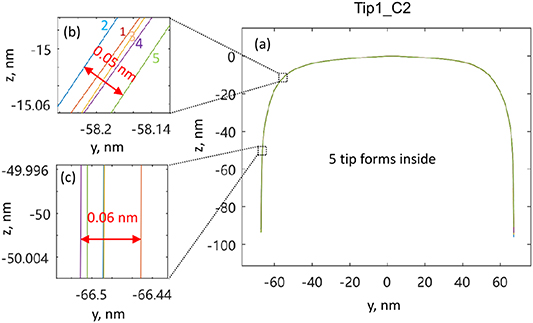
Figure 10. Repeatability of tip reconstruction when 5 repeated measurements are taken on the same tip characterizer by the same tip, shown as (a) 5 averaged tip profiles obtained from 5 repeated measurements, and (b), (c) inset figures show the detail of tip profiles zoomed-in at the marked boxes. A maximum deviation is 0.06 nm is obtained. The sequence of the repeated measurements are marked in (b).
Download figure:
Standard image High-resolution imageThe next goal of the experiment is to investigate the reproducibility of the tip characterization. In figure 11, the results 'Tip1_A1', 'Tip1_B1', 'Tip1_C1' and 'Tip1_C2' are compared. As each result consists of five averaged tip profiles, totally 20 tip profiles are plotted. In this test, the results 'Tip1_A1', 'Tip1_B1', 'Tip1_C1' are obtained before, during, and after the calibration of the user sample, respectively. By comparing these results, we could not only investigate the long-term repeatability of the measurements, but also the tip wear. As the sample and tip characterizers are repositioned when the measurements are carried out, its influence on measurements are included as well. As can be seen in figure 11, the obtained tip profiles show excellent repeatability of below 0.4 nm. It confirms not only the high stability, high reproducibility, but also very low tip wear.

Figure 11. Reproducibility of reconstructed tip geometry when the tip is characterized before, during and after the calibration of the user sample, shown as (a) 20 averaged tip profiles obtained from 20 measurements; (b) and (c) parts of tip geometry are detailed after zoomed-in at the marked boxes.
Download figure:
Standard image High-resolution imageFurthermore, as results 'Tip1_C1' and 'Tip1_C2' are obtained from two different IVPS100PTB samples, the contribution of different tip characterizer are also included in the results. In figure 11(b), the tip profiles obtained from the 'Reference 1' and 'Reference 2' show a slight difference. It may be attributed to the deviation of the corner rounding radii between two different tip characterizers.
As the next step, we compare two results obtained from the user sample 'S_Tip1_A1' and 'S_Tip1_A2'. The results are depicted in figure 12. For sake of comparison, the left sidewall of profiles is aligned, and the right sidewall is zoomed-in at the marked box as detailed in the inset figure, showing a deviation of about 0.3 nm. This deviation is attributed to both the tip characterization and tip correction procedures.

Figure 12. Repeatability of two measured profiles of a user sample after the tip contribution is corrected, shown as (a) averaged profiles of a user sample measured by 'Tip1' in the 'Round A' and 'round B', respectively, are compared. The left sidewall has been aligned; (b) an inset figure showing the slight deviation of the right sidewall of the measured user sample.
Download figure:
Standard image High-resolution imageAfter the investigation with the 'Tip1' is finished, we applied another new CDR120 tip denoted as 'Tip2' for a comparative measurement with the 'Tip1'. The experiment procedures of 'Tip2' are also shown in figure 9. The results of the user sample obtained by two tips are compared after their contribution is corrected. The aim of this comparison is to investigate the reproducibility of the whole measurement.
The results are depicted in figure 13. Again, the left sidewalls of profiles are aligned for sake of comparison. The right sidewalls are zoomed-in in the marked box and detailed in the inset. A deviation of the right sidewall of about 0.9 nm can be seen. This deviation may be attributed to many influence factors, such as the measurement noise, drift, the geometry difference between three sets of tip characterizers, sample repositioning, the algorithm of tip reconstruction and tip correction, etc. However, the agreement of below 1 nm between two sets of measurements performed by two independent tips indicates the high accuracy of the tip characterization method.

Figure 13. Comparison of the profile of user sample measured by two different tips after their contributions have been corrected, shown as (a) two averaged profile of user sample where the left sidewall has been aligned; (b) an inset figure showing the deviation of the right sidewall of 0.9 nm.
Download figure:
Standard image High-resolution image
Based on the investigations mentioned above, we set up a preliminary uncertainty budget of the tip form characterization as summarized in table 1. The main error component is still the uncertainty of tip width calibration.
Table 1. Preliminary measurement uncertainty budget of the tip form characterization.
| Major error sources | Standard uncertainty (u) |
|---|---|
| Uncertainty of the tip width calibration | 0.8 nm |
| Uncertainty of the corner rounding radii of the reference sample IVPS100-PTB | 0.4 nm |
| Short-term stability due to measurement noise, etc | 0.1 nm |
| Long-term stability due to drift, tip wear, etc | 0.2 nm |
| Combined uncertainty (uc) | 0.97 nm |
5. Conclusion
Tip geometry is a fundamental concern in AFM measurements. The image obtained in AFM measurements is the delated results of a sample by the effective geometry of its tip. To derive the real geometry of the sample, the tip geometry must be reconstructed and then be corrected from the measured AFM image.
In this study, a method for accurate tip characterization and tip correction has been introduced in detail. The method applies a tip characterizer based on the sample type IVPS100-PTB, whose geometry and corner rounding have been accurately and traceably calibrated to the lattice of crystal silicon by using high-resolution transmission electron microscopy.
To obtain high accuracy, we have improved measurement strategy and data evaluation methods. The detailed methods have been presented for eliminating the influence of the line width roughness (LWR) of the reference features, as well as the optimization of the tip characterization algorithms concerning the aspects such as the measurement noise, averaging of tip geometry and point density.
A detailed experimental study has been carried out in investigating the measurement performance of the development methods. In the first step, the repeatability of tip characterization has been verified. For an AFM image where 5 × 8 tip profiles has been obtained, the standard deviation of individual tip profiles is small as 0.5 nm. The standard uncertainty of the averaged tip profile can be further reduced owing to the averaging effect to 0.08 nm. In the second step, the tip form is characterized and compared before, during and after calibrations of a user sample. The agreement of 20 averaged tip profiles reaches 0.4 nm. The results thus confirm the high measurement stability, low tip wear as well as the high measurement consistency between two tip characterizers. At the third step, two measured results of a user sample obtained by the same tip in two different measurement runs are compared after the tip contribution has been corrected, showing an agreement of approximately 0.3 nm. It indicates the excellent performance of the tip characterization and tip correction method. Finally, the results of the user sample measured by using two independent tips are compared, indicating an agreement of 0.9 nm.
The developed method could be not only applied for characterizing tip geometry of CD-AFM which has a flared tip shape, but also extended for characterizing of normal AFM tips with either a conical or pyramidal tip shape. We will extend our algorithm for this application in near future.
Acknowledgments
This project has received funding from the EMPIR programme co-financed by the Participating States and from the European Union's Horizon 2020 research and innovation programme.