


Abstract
Dimensional surface metrology is required to enable advanced manufacturing process control for products such as large-area electronics, microfluidic structures, and light management films, where performance is determined by micrometre-scale geometry or roughness formed over metre-scale substrates. While able to perform 100% inspection at a low cost, commonly used 2D machine vision systems are insufficient to assess all of the functionally relevant critical dimensions in such 3D products on their own. While current high-resolution 3D metrology systems are able to assess these critical dimensions, they have a relatively small field of view and are thus much too slow to keep up with full production speeds. A hybrid 2D/3D inspection concept is demonstrated, combining a small field of view, high-performance 3D topography-measuring instrument with a large field of view, high-throughput 2D machine vision system. In this concept, the location of critical dimensions and defects are first registered using the 2D system, then smart routing algorithms and high dynamic range (HDR) measurement strategies are used to efficiently acquire local topography using the 3D sensor. A motion control platform with a traceable position referencing system is used to recreate various sheet-to-sheet and roll-to-roll inline metrology scenarios. We present the artefacts and procedures used to calibrate this hybrid sensor system for traceable dimensional measurement, as well as exemplar measurement of optically challenging industrial test structures.
Export citation and abstract BibTeX RIS

Original content from this work may be used under the terms of the Creative Commons Attribution 3.0 licence. Any further distribution of this work must maintain attribution to the author(s) and the title of the work, journal citation and DOI.
1. Introduction
3D microscale structure or geometry is increasingly being exploited to improve performance of (or add functionality to) macroscale parts, such as those found in large-scale optics, as well as in weld structures on automotive parts and structured surfaces on bearings [1]. The same is true for smaller parts fabricated in a highly parallel fashion on large or continuous substrates in sheet-to-sheet (S2S) or roll-to-roll (R2R) manufacturing processes, such as radio-frequency identification (RFID) tags or disposable medical devices [2, 3].
Cost effective advanced manufacture of such items demands low-overhead, high-throughput in-process metrology and inspection to ensure the tight tolerances on these parts are met. Traditional machine vision solutions are increasingly becoming insufficient for the task due to limited resolution and lack of 3D measurement capability [4, 5]. Consider the screen-printing of metallic conductors (fingers and busbars) onto amorphous-silicon photovoltaic (PV) wafers (figure 1). In a typical electronic screen-printing process, a form of additive manufacturing, a metallic conductive paste is deposited along the intended conductive pathways through a patterned mask that is finely perforated. Heat or a chemical process is then used to cure the paste, thereby setting the final electronic properties of the conductor. Features of different size, in this case the fingers and busbars, may be printed separately in a two-stage process. The electronic performance of this PV system strongly depends on the quality of the conductor deposition and curing processes. Relative misalignment of busbars and fingers in the two-stage deposition (figure 1(a)) represents a simple but catastrophic open-circuit defect typically requiring the wafer to be scrapped. Current state-of-the-art 2D machine vision is capable of detecting and even measuring this misalignment at process speeds, and is used in industry. However, other progressive defects in the printed electronics, such as the quality of the cure, while possible to detect in a coarse fashion by a functional test, can only be understood using 3D topography data (figure 1(b)). Position correlations between line resistivity and surface morphological parameters such as electrode cross-section geometry and local topography have recently been demonstrated in an offline study [6] (see also [7]). The value of 3D over 2D in-process measurement has also been demonstrated for other applications, such as particulate contamination in organic photovoltaics [8].

Figure 1. High-resolution image of a defective 160 mm × 160 mm PV wafer provided by Applied Materials Italia, containing three vertical 'busbars' and approximately 100 horizontal 'fingers'. Insets: Zoomed detail of (a) mask alignment defect, (b) busbar/finger node topography.
Download figure:
Standard image High-resolution imageIt is non-trivial to achieve large-area, high-resolution 3D inspection at machine-vision throughputs due to the high dynamic range (HDR) challenge [4]. State-of-the-art implementation of 3D techniques may account for perhaps two of the four to five orders-of-magnitude throughput increase required (see figure 2); wavelength scanning interferometry and dispersive interferometry are promising examples [9, 10]. The remaining increase must be solved by using smarter measurement strategies exploiting a priori information about the inspection process to only measure where and when it is needed.
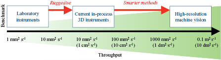
Figure 2. Step-changes in measurement throughput required for advanced manufacturing processes.
Download figure:
Standard image High-resolution imageSuch a measurement strategy can be implemented by hybridising 2D and 3D sensor systems. Features of interest/likely importance can be detected and located using a coarse high-throughput sensor such as 2D machine vision, and then subsequently prioritised and selectively measured using a high resolution 3D sensor guided by advanced routing algorithms [4, 11] (see figure 3). Prioritisation involves ranking of features by significance, weighted according to the time or energy burden of visiting that feature accounting for the finite inspection resources available to the hybrid system.
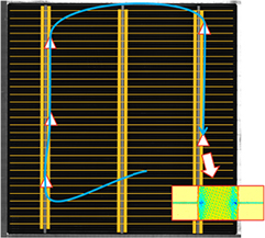
Figure 3. Hybrid 2D/3D measurement of a PV wafer: fast 2D image (background), feature recognition (yellow), route-planning (blue), followed by localised high-resolution 3D measurement of priority features (triangles, with example data inset).
Download figure:
Standard image High-resolution imageIn this paper, we present such a hybrid 2D/3D inspection system, installed on a lab-based simulation platform that can recreate a variety of inline inspection scenarios and introduce the developed measurement strategies and smart routing optimisations. Calibration methods and the traceability considerations for such systems are then discussed. Finally, we apply the system to two printed electronics test cases with unique manufacturing scenarios.
2. Hybrid 2D/3D inspection concept
Implementations of the hybrid 2D/3D inspection concept for R2R and S2S processes are summarised in figure 4. In the case of R2R, a continuously moving substrate passes under an array of machine vision cameras that image the substrate; as the web continues there is a finite opportunity to identify features of interest in the image stream, triage these, and arrange for a downstream 3D sensor to rendezvous with each feature in turn. In the case of S2S, there is slightly more flexibility to visit features of interest with the 3D sensor. Figure 4 encapsulates a variety of measurement and engineering challenges, including those out of immediate scope for sensor module development, such as the logistical challenges of precision web steering and axial flutter management in the case of R2R and the precision substrate handling required for inspecting many substrates in the case of S2S. It is more efficient to separate those challenges in a controlled way.
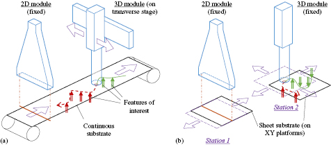
Figure 4. Schema summarising the hybrid 2D/3D inspection concept for (a) an R2R process and (b) a S2S process. Components for substrate steering and vibration control are not shown. Note that relative sensor-sample motion is largely equivalent between both processes.
Download figure:
Standard image High-resolution image2.1. 2D module: imaging system and illumination strategies
2D machine vision is a very mature technology [12] and many off the shelf systems are available. Here we have chosen to implement a state-of-the-art 2D machine vision system comprising of a line-scan camera (8160 px × 1 px, 80 kHz line rate) equipped with a telecentric imaging system (180 mm width of view, i.e. approximately 22 µm in sample space per pixel). Telecentric optics provide a constant magnification image of an object, making calibration and linking of coordinate systems in the hybrid sensor more straightforward. Position referencing encoder-or reference interferometer-based triggering can be used to enable line-wise assembly of a high-resolution 2D image during an acquisition in the case of R2R and S2S, respectively. By default, an isotropic image is acquired but anisotropic sampling strategies are feasible. The high camera line-rate permits sub-pixel motion blur for substrate velocities up to 1.7 m s−1, subject to sufficient illumination intensity. Various illumination options are possible including bright- and dark-field illumination from an LED source impinging on the sample directly or via a large plate beam-splitter (see figure 5); further optimisation using spectral and polarisation filters is possible with this setup.

Figure 5. 2D machine vision component installed on simulation platform with schema showing potential illumination configurations.
Download figure:
Standard image High-resolution imageThe data acquired from the 2D module is first used to detect features/defects and create a listing of all points of interest (POI) for potential local 3D measurement. To detect features we employ various edge detection [13] and cross-correlation methods in combination with a priori print design information. This information is then used for registration in a model-based defect detection algorithm [5] that compares optical response of the product with a modelled optical response. Data from this model-based method is then used to assign each POI a process-relevant score indicating the inspection desirability attached to the defect. This score is linked to the defect's specific functional significance that is derived from proprietary process-specific information obtained by functional correlation studies that may be performed both offline prior to manufacture, and online in a continuous training process, correlating data from functional acceptance tests and any through-life metrology with the inspection data obtained and stored by this system.
2.2. 3D module: form and local topography measurement
Items that may appear to be effectively planar within a high-resolution 3D sensor's field of view (FoV) often have a significant macroscale form. For thin objects, such as a PV wafer, this is dominated by deformation due to fixturing and self-weight, and may not necessarily be predicted from a design (see a solid 3D workpiece). This can result in vertical displacements beyond the axial working range of a typical 3D sensor.
As exemplified in the case of the PV wafer example, to obtain an appropriate level of optical signal to measure both the highly-reflective silver electrodes and the highly-photoabsorbing active surface, the acquisition parameters of the sensor must be adjusted. Reactive auto-adjustment methods are available on some commercial 3D sensors but have a finite response time and are best suited to stepping between extended regions of fixed reflectivity since potentially important data from regions of the intensity step change may not be measured. Reactive methods are also inappropriate for the measurement of small, sparse features with a vastly different optical response to their surroundings.
Therefore, to enable the use of 3D sensors with finite axial (vertical) working range and limited dynamic sensing range, we suggest that the initial 2D feature detection is supplemented by coarse form measurement and intensity mapping. In this way, when a 3D sensor arrives at the 2D location of a feature of interest, the sensor may be vertically pre-aligned with acquisition parameters preconfigured for optimum intensity gain/exposure (sensing technology dependent). Such a system could then be considered as HDR in both a dimensional (defect size/throughput ratio) and an optical sense (high-to-low reflectivity ratio). This proactive compensation technique may be also adapted for other optical systems, such as photo-electronic property mappers [8] or point scatterometry systems [14], or as a complementary feedback route for laser machining processes [15].
Coarse form measurement is achieved using a chromatic confocal point sensor [16] (Precitec Chrocodile-E, 3 mm working range). To acquire a full form measurement the sample may be moved in a raster pattern under the confocal probe, with location dependent triggering supplied from the position referencing system. Faster 3D optical scanner techniques such as laser triangulation sensors [17, 18] would enable faster uniform measurement of an extended area as would be required in the case of R2R, but one or more point probes may provide a cost-effective alternative when used with intelligent sampling strategies linked to a priori defect models and feature design information [19, 20].
Localised high-resolution surface topography measurement is acquired using a STIL MPLS180 Nanoview line sensor, also employing the chromatic confocal principle. This line sensor may be considered as an array of 180 parallel optical profilometers on a 7.4 µm pitch. The line sensor has a line-rate of 1.8 kHz, corresponding to about 13 mm s−1 throughput for an isotropic sampling grid. Exposure time and LED intensity may be adjusted to suit specific measurement requirements. As with the other sensors triggering is provided by a position referencing system.
The coarse form measuring point sensor is positioned ahead of the local surface topography measuring line sensor. The sensors are attached to a 50 mm travel vertical stage for vertical pre-alignment (Thorlabs LNR50SE, see figure 6).
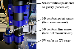
Figure 6. 3D measurement components on vertical positioner.
Download figure:
Standard image High-resolution image2.3. Smart routing optimisation: defect triaging and trajectory planning
Successful implementation of the hybrid 2D/3D measurement strategy requires efficient pruning of potential 3D measurement targets or POIs based on ranking of process-relevant POI scores, combined with hardware-appropriate trajectory planning. We call this iterative process of POI pruning and route-planning 'smart route optimisation' since the initial ranking of POIs may radically change based on their location, proximity and the parameters of the dynamic inspection system. In this section, we describe a general method to optimise the inspection of a pre-existing ranked list of scored POIs with the 3D sensor, while under different realistic scenarios.
We suggest that the typical goal of measurement route optimisation is to maximise the 'thoroughness' of the inspection, whilst respecting defined budgets of time or energy. The precise meaning of 'thoroughness' would be context specific, and linked to the inspected process itself; a very simple example would be the total count of unique POIs visited. Further constraints must also be applied to the optimisation to account for finite variation of motion system parameters, ranges of travel, and so on. In particular, the dynamics of this inspection process mean that small changes in the initial conditions of the sensor can introduce large changes in the final optimised route for a given set of targets. Furthermore, for inspection of continuously moving substrates in a R2R process, it becomes impossible to inspect multiple non-overlapping POIs aligned transversely across the substrate with a single sensor on a single transverse motion stage. In this case, smart routing optimisation can easily be extended to take in to account multiple sequential sensors down a production line in order to approach 100% inspection of relevant defects.
General routing algorithms such as the travelling salesman problem (TSP) provide a basis for computing the order of visits to the set of POIs as nodes; node separations would be calculated in terms of required time or energy expenditure. By also assigning a proportionate reward for the successful visit to a given node, it is possible to attempt to increase the total reward or score by pruning low-value, high-cost nodes from the route. The basis for the smart routing algorithms developed for this work is the Mathworks TSP example [21, 22]. Major changes implemented in our new algorithm are summarised in order of importance in the remainder of this section. Standard TSP terminology such as 'city' and 'trip' are used figuratively in the explanation.
2.3.1. Cost function to minimise.
The optimiser no longer seeks to minimise the 'distance' or resource expenditure of each trip in the tour. Instead, the optimiser now seeks to maximise the total reward earned for the tour. The total reward is the cumulative sum of the reward earned for visiting each trip's destination node (or rather, the associated physical POI). Written equivalently as a minimisation, the optimiser now seeks to minimise the total rewards abandoned from a calculable maximum by choosing not to visit a given POI. Since total resource budgets must still be respected, an inequality constraint is added for each finite resource (such as time or energy), such that the total expenditure for a given resource remains less than a specified limit.
2.3.2. New constraints for measurement speed boundary condition.
In order to generate areal surface topography maps from the 3D line scan measurements with data arranged on an easy to process nominally orthogonal grid of points, velocity boundary conditions are applied to ensure that the line sensor arrives at the start of the local 3D measurement associated with a given node (a) at the required measurement speed and (b) from a direction parallel or anti-parallel to the required scan direction (see figure 7); that is, moving with fixed speed either up or down the scan axes, and stationary in the step axis. This has the advantage of reducing acceleration-induced errors. For the purposes of the optimisation, each POI is now represented by two co-located nodes, representing the parallel and anti-parallel measurement direction options, respectively. A new inequality constraint is added for each such co-located pair of nodes to allow a visit to, at most, one node of each co-located pair in the solution. To enable automated pruning of POIs, inequality constraints are used, in place of the equality constraints in the original algorithm that enforced exactly one visit to every POI.
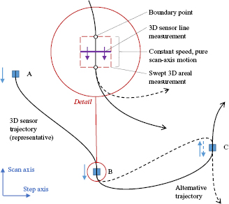
Figure 7. Velocity boundary conditions imposed by operation of 3D line sensor. Within each swept areal measurement (A)–(C), sensor motion must be (anti-)parallel to the scan axis at a defined constant speed (see point (B)). There is a binary choice available at each node, to optimise the onward motion (see point (C)).
Download figure:
Standard image High-resolution image2.3.3. Calculation of trip resources.
To complete the optimisation, the resource expenditure must be estimated for each potential trip. The fixed-speed, binary direction velocity boundary conditions associated with the 3D line sensor conveniently disconnects each tour for independent calculation.
The trajectory is calculated according to the end goal of the optimisation. In the case where time is limited, rewards are maximised by taking the shortest-duration trajectory for any given trip. The minimum time trajectory between two points consist of a maximum acceleration phase to a maximum linear velocity, a constant maximum-velocity transit phase, and a maximum deceleration phase to the end point velocity. Maxima for acceleration and velocity are typically constrained to minimise dynamic forces on system components, and to limit vibration or other disturbances of the metrology frame. In the case where energy is limited, rewards are maximised by prioritising high value targets lying on paths requiring minimal changes in velocity. The velocity boundary condition implies that an optimal tour would involve chains of high-value targets aligned parallel to the scan axis. To calculate energy expenditure, it is assumed that kinetic energy is not recovered during a braking manoeuvre, nor transferred between independent axes of a Cartesian motion system during a change in direction. These assumptions are reasonable for standard industrial motion systems. Since the initial, transit and final velocity of each Cartesian motion axis is known, the total energy spend is the sum of magnitudes of two changes in kinetic energy for each axis. Additional terms may be added to account for rate- and path length-dependent losses, according to information available for a given motion system.
2.3.4. Miscellaneous data cleansing.
Prior to node generation, any clustered POIs that could fit within a single measurement FoV of the local 3D sensor are replaced with a single POI in the geometric centre of the cluster. The new POI is assigned the cumulative score of the replaced cluster.
2.3.5. Simplifications for the R2R method.
The optimisation is modified in the case of inspection of a substrate moving with fixed speed under an inspection sensor on a transverse motion stage—typically the case with roll-to-roll manufacturing methods. Since the scan axis velocity is fixed, each POI can be represented by a single node. Resource expenditure calculations are modified to include only the transverse motion axis of the sensor. Impossible journeys, such as those requiring the transverse axis to exceed a specified speed limit, can be deleted or new equality constraint added to sum these to zero. A typical impossible journey would be between two locations collocated in the machine direction but separated in the transverse direction.
3. Lab-based simulation platform
It is helpful to develop and test new sensors and measurement strategies in a controlled environment that (a) puts aside irrelevant challenges, such as sample manipulation and the high per-run starting cost in R2R, and (b) replicates true process conditions in a deterministic way. Therefore, we developed the above hybrid 2D/3D inspection concept on a platform that can simulate aspects of both R2R and S2S processes by exploiting the equivalency of the relative motion of sample and sensor in both classes of process (see figure 4). A fast two-axis motion system (Aerotech PRO165/PRO255 in XY configuration; linear motors; 500 mm s−1 maximum speed) with Abbe-optimised interferometric displacement metrology translates a sample fixture laterally relative to a sensor gantry supporting sensors (see figure 8). In the case of R2R, it is simple to assign one of these axes to simulate the constant linear web motion while the other orthogonal axis can be used to simulate the lateral motion of the 3D sensor across the web. A single gantry is used for the mounting of sensors reducing the travel range required by the stage. The absolute position of sensors above the gantry is only constrained by the required FoV and the velocity/acceleration required for the simulated R2R process and simulated motion of the 3D sensor. A pause in the simulation is used in order to translate and bring the sample up to the simulated web velocity before passing under each of the different sensor subcomponents of the hybrid 2D/3D system. In the case of S2S, the sensors are placed as close to the centre of the two-axis stage in order to maximise the physical space available for the routing algorithm trajectory calculations. It is also possible to introduce simulated vibration, lateral drift and vertical flutter by encoding these effects in to the stage controller. This enables the assessment of the tolerance of a sensor system to such effects in a highly controlled manner.
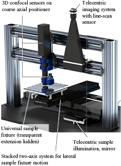
Figure 8. Rendered representative image of the lab-based simulation platform, showing an example configuration for a hybrid 2D/3D inspection system.
Download figure:
Standard image High-resolution image3.1. Sample fixturing
The simulation platform supports a number of methods for samples support and fixturing, via a common tilt-adjustable base (see figure 9). A vacuum chuck is used to fix thin flexible or semi-rigid items into a well-defined measurement plane, reducing out-of-plane surface tracking and improving collision avoidance reliability. Repeatable in-plane alignment and position referencing was implemented using universal fixturing principles reported previously [23]. Use of a common fixturing system simplifies and speeds up fusion or comparison of measurement data from multiple instruments within a defined workflow, and is consistent with the 5S methodology, one component of lean manufacturing [24]. Samples with well-defined geometry and sufficient later stiffness, such as amorphous-silicon PV wafers, may be repeatably installed using only a side fence, realised here using precision steel rules. For routine or significant one-off measurements campaigns of features on flexible, easily deformed films, extracted film pieces with poor edge definition may be semi-permanently attached to identical thin, stiff square substrates, for handling as for a PV wafer. We also implemented a more pragmatic approach to universal fixturing to promote wider adoption, using a system of interchangeable plates available from Thorlabs (MLSP series). Finally, with the vacuum chuck removed, there is a volume available to mount small non-planar parts or calibration artefacts on an appropriate translation/rotation adjustment stack.
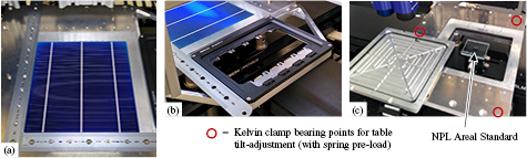
Figure 9. Sample fixturing options: (a) wafer on removable vacuum chuck with removable fence; (b) universal fixture using interchangeable plates; and (c) calibration artefact on adjuster stack.
Download figure:
Standard image High-resolution image3.2. Traceable reference interferometry
The internal stage encoders are supplemented by external (reference) laser displacement interferometry where required (Zygo ZMI 2001 series; see figure 10(a)). FPGA-based control of a custom backplane, developed for the NPL Areal Instrument [25], optionally enables mutually- and externally-synchronised multi-axis spatial triggering. To partially mitigate the Abbe error associated with the vertical offset of the inspection plane, the reference interferometer measurement-arm retroreflectors are attached directly to the underside of the sample holder tip/tilt thrust plate, the uppermost fixed component in the sample stack. Beam paths are directed directly under the centre of the vacuum chuck. Stage motion is limited to a single axis whilst reference interferometry is used, to avoid the requirement for costly and bulky plane mirror blocks typically required to directly measure two-axis motion of an object [25]. Alternatively, motion of the two stacked drives may be done separately, as in figure 10(b).
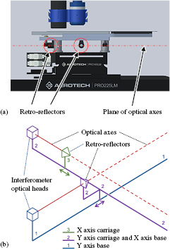
Figure 10. Abbe-compensated reference displacement interferometry: (a) direct measurement of sample table XY position for single-axis motion; (b) partially indirect measurement supporting full planar motion range.
Download figure:
Standard image High-resolution imageWe previously reported [26] an example application, in which the reference interferometer provided an independent estimated position of a grating-instrumented film, for the testing of a sub-micrometre accuracy substrate tracking metrology for precision R2R processes. This example also demonstrated the secondary function of the simulation platform as an instrument development host.
3.3. Software implementation
Automation and control software implementation consists of several semi-autonomous actors distributed over two PCs (basis: NI LabVIEW). Each actor manages one item of hardware via the supplier's API. A coordinator module interacts with each actor to carry out scripted tasks, monitor progress and collect returned data. The distributed architecture reduces the resource load on each machine, thereby relaxing the PC specifications required; the architecture also permits additional support for other temporary sensors hosted by the demonstrator. Repetitive low-level handshaking and triggering, such as move completion signalling, is done directly between actors. Appropriate metadata is automatically stored with measurement data, for traceability and to simplify documentation and reporting. Alignment is planned toward one or more standardised metadata formats such X3P [27], SDF [28] or QIF [29].
4. Sensor calibration
Motion is programmed and measured in motion system coordinates, specifically the XY and Z drive encoders. The drive encoders are pre-calibrated by comparison to the reference interferometer (for XY) and calibrated step artefacts (for Z). In situations where increased lateral displacement metrology is required, the reference interferometer is used directly. To enable conversion mapping of locations between sensors, the global offset of each sensor is determined. Each sensor is centred on each of between one to three datum markers on the sample platform, and the corresponding stage offsets recorded. The relative position of the nominal centre of the sample space is also calculated, and the full set of offsets applied automatically by the coordination software. Remaining calibration activities are limited to the self-contained metrological characteristics of individual sensors. Such calibration activities are described in this section for the permanent sensor modules.
4.1. 2D machine vision sensor
Calibration of the line-scan camera sensor consists of (a) traceable characterisation of the image scale along the pixel line; (b) measurement of, and optional correction for, undesirable tilt or roll of the camera FoV; and (c) estimation of the final effective lateral resolution for a stationary object. To guard against malfunction of the stage or triggering timing, the lateral scale in the scanned direction of an assembled 2D image is also verified.
The adjustment and calibration procedure makes use of an ISO 12233-consistent camera calibration artefact (CCA) developed specifically for line-scan cameras and reported separately [30]. In brief, the CCA (shown in figure 11) consists of a 120 mm × 20 mm feature field designed to enable, without motion, estimation of absolute XY location and roll about Z, as well as the MTF of the line-scan camera. Additional features on the CCA assist the operator with coarse initial alignment. Using this method, the mean pixel spacing of the camera was estimated to be 21.84 µm ± 0.03 µm. Roll about Z results in a shear distortion on an assembled 2D image.
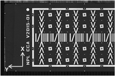
Figure 11. NPL CCA, installed horizontally against a sample fence to adjust and calibrate the Y scale of the linescan camera imaging system.
Download figure:
Standard image High-resolution image4.2. 3D chromatic confocal sensors
The chromatic confocal point sensor (the probing system) and the XY stage (the lateral scanning system) combine to form an areal surface texture measurement instrument, whose metrological characteristics may be calibrated according to ISO 25178-602 [31]. For the areal instrument incorporating the line sensor, the step axis of the lateral scanning system is assembled from a series of Y-aligned line acquisitions arranged along Y; that is, every 180 steps along the step axis are measured simultaneously as the 180 channels of the line sensor. Stitching is done using only the stage encoders, not from overlaps in measurement data.
Metrological characteristics to be calibrated for each sensor as a measuring instrument include amplification coefficients for the X, Y and Z scales; flatness; static and dynamic noise; and some measure of spatial resolution such as the width limit for full transmission of an application-matched height [31]. For brevity, we present here the in situ calibration and verification procedures that differ from the general methods to calibrate metrological characteristics discussed elsewhere [32–34].
The XY stage encoders, which measure the relative motion of each sensor over the sample, are calibrated by comparison to the reference interferometer. This calibration provides the lateral amplification coefficients for the two 3D sensors, if combined with a traceable description of the relative spatial relationship between the line sensor's 180 parallel measurement points. This relative spatial relationship is determined by comparison to the XY stage encoders and the line sensor's internal axial (Z) scale. The line sensor's internal scale using PGR features at a number of positions within the working range of the sensor.
A discussion of the chromatic confocal line sensor's inter-channel spatial relationship follows; for clarity, analysis is presented for a single wavelength corresponding to the centre of the probing system's working range. As summarised in figure 12, the nominal positions of the points are distributed with a uniform spacing  along a mean centreline, which may be slightly rotated from the Y-axis (by
  ,
,  ). These rotations are deliberately minimised during installation and are assumed to be small, such that small-angle approximations may be applied. Successive line acquisitions remain centred on the Y-axis, so that the small rotation from the Y axis forms a saw-tooth pattern in the residuals. The true centre of each focal spot is then further displaced from the mean centreline. The true position Xj of the centre of the working range of the
  th point in the set is then given by
where  is the global position of the midpoint of the mean centreline,
  is the number of points (i.e. 180), the term in
  represents the mean centreline and
  represents the pointwise residuals to the mean centreline. In terms of global topography measurement error, the mean centreline describes with respect to the Y-axis the mean sampling interval in Y (i.e.
  ), as well as any roll (
 ) or tilt (
 ) misalignment. Similarly,
  can be subtracted from subsequent data corrections;
  is effectively the flatness deviation of the line sensor. Where line sensor data is expected to be patched together in Y, sensor Y steps are programmed in exact multiples of
  to simplify data fusion.

Figure 12. Analysis of nominal and actual position of the  th measurement point of a 3D line sensor, and hence the relative spatial relationship of the full set. Not to scale.
Download figure:
Standard image High-resolution imageBy moving the global reference point from the centre to the start of the measurement,  , (1) can be simplified to a constant term, a
  -dependent centreline term, and the point-wise residuals:
To quantify the unknown parameters, a position estimate  is obtained for each point in
  , and nonlinear least-squares line fits applied to the position estimates. Position estimates were obtained experimentally using the following procedure, which required only a single step height calibration feature. An NPL Areal Standard artefact [35] was mounted onto a tilt-adjustment stack with the vacuum chuck removed (see section 2.1), so that the Areal Standard top surface was a few millimetres above the main sample table. The Areal Standard was adjusted to reduce tilt such that the complete chip remained within the 100 µm working range of the line sensor. To estimate
  and
and  , the lateral scanning system was configured to scan along the Y-axis (the conventional step axis, that is, nominally collinear with the point array, see also figure 13). The sampling interval in Y was set to be much smaller than the nominal value of the Y sampling interval, i.e.
  (1 µm and 7.45 µm, respectively). The measurement location was centred on a 2 µm depth PGR feature (a step height standard, see [36]), and scan length set to greater than the sum of sensor line width (1.35 mm) and three widths of the PGR feature (grand total 1.67 mm). Thus, each of the 180 channels measured a profile containing the PGR feature and the adjacent regions required for an ISO 5436-1:2000-compliant step height calculation [37]. This was repeated ten times. Values for
  were taken as the mean Z over all repeats of all points in the three flat step height calculation regions used for the
  th point step height. Each value for
  was taken as the centre of mass in Y of the
  th point step height. A non-linear least-squares line fit to the set of
  and
and  yielded estimates for
  and
and  , respectively by equation (2). To estimate
  , the lateral scanning system was then configured for a conventional areal measurement with sampling intervals of 1 µm and
  in X and Y, respectively. The measurement was centred on the 2 µm PGR feature as before, with a measurement size of three times the PGR feature X dimension (total 600 µm) in the X direction and at least
  in the Y direction. This configuration ensures that at least one set of n collinear profiles across the PGR feature can be extracted comprising one from each channel of the line sensor. These collinear profiles nominally describe the same physical line across the feature; apparent differences can be attributed to relative misalignment of points. Each value for
  was taken as the centre of mass in X of the step height from the
  th profile. A nonlinear least-squares line fit to the set of
  yielded estimates for
  by equation (2). Note that this method avoids the need to provide a well-formed, perfectly Y-aligned step feature as wide as the line sensor, but at the expense of an
  -fold increase in measurement time. Further, if the PGR feature height is well matched to the user's measurement task, the measurement data above can also be exploited to verify the scales of the complete XYZ motion system.

Figure 13. Areal topography (left) and confocal intensity maps (right) of the 2 µm PGR feature, acquired by rastering the 3D confocal point sensor. The line-sensor measurement line is nominally left-to-right in this view. The crossed red lines indicate the paths swept by the line-sensor to characterise its inter-channel spatial relationship. Topography of an edge (purple box) is used to estimate the spatial resolution.
Download figure:
Standard image High-resolution imageTypical methods used to estimate the spatial resolution of a topography measuring instrument involve 3D Siemens stars or linear gratings [34]. Rotated reflectivity edges are used to estimate the spatial frequency response of a conventional camera [30]. Noting the implementation constraints on in situ calibration of industrial metrology, we supplemented the conventional method with an approach using the tilted edge of the 2 µm PGR feature (see figure 13). The edge quality and profile of the PGR feature was first measured using a reference instrument, to qualify the assumption that any two parallel profiles across the feature edge are equivalent. Then, an areal measurement of the tilted edge could be used to construct a super-sampled profile of the edge response of the confocal sensor under calibration. The edge response function can be converted to a modulation transfer function (MTF), an indication of the sensor spatial resolution for features of 2 µm height. This compromise method can be applied to detect changes in sensor resolution during in-process use.
5. Experimental results
The utility of the hybrid 2D/3D inspection system has been demonstrated on two industrial test samples with known defects. The first example concerns the screen-printed PV test wafer described in section 1. The test wafer was placed on the sample platform against the edge fence and the vacuum chuck enabled. A high-resolution 2D image was acquired as per section 2.1, using bright-field illumination (image was used to generate figure 1). Standard image processing methods were developed to highlight the fingers and busbars; the location of breaks in the busbar/finger nodes were detected by model-based defect detection [5]. The 2D image was also analysed by applying a 50 × 50 window maximum-value filter to the 2D preview region occupied by the wafer to create a coarse intensity map describing the reflectivity of the surface (see figure 14). The 3D point sensor then measured the coarse form of the wafer, as fixed on the vacuum chuck (see figure 15). By interrogating the coarse form and reflectivity range maps, the high resolution 3D line sensor was vertically pre-aligned with its acquisition parameters pre-configured to efficiently acquire 3D measurement of an optically-challenging feature with high and low reflectivity elements (see figure 16). The composite of just two measurement passes with pre-optimised illumination intensities yielded a clear measurement of the open circuit defect.

Figure 14. Coarse map of surface reflectivity range PV test wafer.
Download figure:
Standard image High-resolution image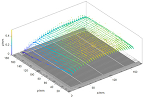
Figure 15. Coarse form map for the PV test wafer. Note that the vertical range of the form is approximately four times the 100 µm working range of the 3D line sensor.
Download figure:
Standard image High-resolution image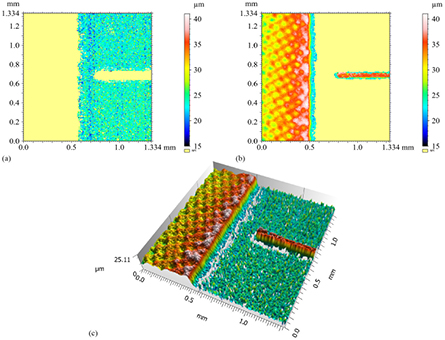
Figure 16. Patched local high-resolution measurements of a feature on the PV test wafer: (a) the photoabsorber surface, acquired at high illumination intensity; (b) the conductor, acquired in a second pass at 0.5% of the previous intensity; and (c) the patched topography.
Download figure:
Standard image High-resolution imageThe second example again relates to printed electronics and considers a silver screen-printed test pattern on a transparent polymer, provided by VTT, Finland and used in, e.g. disposable medical sensors or logistics labelling. The test pattern was taped onto the vacuum chuck which was then activated. The high-resolution bright-field 2D image (see figure 17) shows some local darkening with film curvature, indicating minor particulate contamination under the film in this informal demonstration. A feature of interest was arbitrarily chosen for high-resolution 3D measurement. The result of the preparatory form measurement, conducted with an abnormally high grid density only for visualisation purposes, is shown in figure 18. The confocal point sensor failed to detect the upper film surface, returning the apparent position of the vacuum chuck instead. Provided this effect is recognised, and film thickness and refractive index are known, the likely film top surface position can be inferred. A series of measurements were pre-configured and undertaken (figure 19); using context-driven rules, good topography segments were extracted and assembled into an areal map describing the conductor, the film upper surface, and the vacuum chuck surface below (figure 20).

Figure 17. Bright-field machine vision image of a silver-printed transparent test pattern on transparent polymer (supplied VTT, Finland). Inset: Location of the feature subject to 3D measurement reported here.
Download figure:
Standard image High-resolution image
Figure 18. Form map for the transparent test pattern. The confocal point sensor detected the top surface printed ink, and the surface of the vacuum chuck supporting the transparent film.
Download figure:
Standard image High-resolution image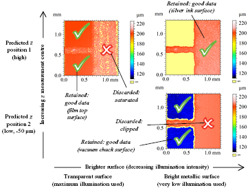
Figure 19. Summary of measurements undertaken on a feature of interest on the transparent test pattern. A global absolute Z scale is used. Tick (✓) and cross (×) icons indicate retained topography segments. No correction for the film refractive index has been applied.
Download figure:
Standard image High-resolution image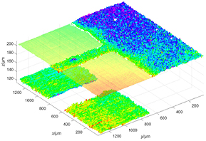
Figure 20. 3D visualization of the patched feature topography from figure 19. The lower surface is plotted with a separate colour scale. No correction for the film refractive index has been applied.
Download figure:
Standard image High-resolution image
6. Conclusions
We have presented a hybrid 2D/3D inspection concept for in-process metrology, which combines a small field-of-view, high-performance 3D topography-measuring instrument with a large field-of-view, high-throughput 2D machine vision system. It was shown how to exploit a state-of-the-art 2D machine vision system to locate features with critical dimensions and defects and how to apply smart routing optimisation and high-dynamic range measurement strategies to configure the acquisition parameters of a 3D sensor proactively for efficient measurement of local surface topography exactly where and when it is needed. Due to the prevalence of 2D machine vision in production lines, this hybridised inspection concept can potentially be implemented by simply adding a 3D system with motion control to the existing hardware, reducing the cost of uptake.
The hybrid 2D/3D inspection concept was demonstrated for the inspection of screen-printed electrodes on photovoltaic Si wafers and screen-printed electronic interconnects on plastic film using a simulation platform that accurately recreates the appropriate inline metrology scenario for sheet-to-sheet or roll-to-roll production by exploiting relative motion and traceable position referencing metrology. We have also presented the artefacts and procedures used to calibrate this hybrid sensor for traceable dimensional measurement, including methods to efficiently verify the scales and spatial resolution of the component sensors. Finally, we have demonstrated efficient measurement of bright conductors on dark or transparent pseudo-planar surfaces, that is, with HDRs of both height and reflectivity; the demonstration included the accurate patching of multiple measurements using only position referencing metrology.
Acknowledgment
The parent project 14IND09 MetHPM (see [38]) is delivered under the EMPIR initiative, which is co-funded by the European Union's Horizon 2020 research and innovation programme and the EMPIR Participating States. Industrial test samples courtesy of project partners and collaborators. We thank the experts in the MetHPM consortium for their valuable input and feedback.