


Abstract
Microwave imaging (MWI) is a noninvasive diagnosis method, which has been investigated for a wide range of applications. MWI techniques include radar-based approaches as well as microwave tomography (MWT). One major challenge designing broadband MWI systems is the development of a data acquisition unit that allows for fast broadband scattering parameter measurements with a high measurement precision and a high dynamic range (DR), at reasonable cost. The cost-performance criteria cannot readily be achieved using commercial, continuous wave (CW) vector network analyzers (VNA) or pulse-based systems. Therefore, in this paper we propose a data acquisition unit, based on the well-known method of frequency modulated continuous wave (FMCW) network analysis. It offers fast scattering parameter measurements without compromising the measurement precision and the DR, and is particularly advantageous for MWI systems requiring a high number of frequency samples. A 2-port metadyne prototype electronics with low hardware complexity was developed, which allows very fast, precise, and accurate reflection and transmission measurements in the frequency range from 0.5 GHz to 5.5 GHz. To the best of the authors' knowledge, a system with combined performance in terms of bandwidth, sweep time (1 ms), DR (80 dB) and maximum signal-to-noise-and-spurious ratio (65 dB) has not previously been reported. The design, the calibration, and the characterization of the prototype electronics are described in detail, and the measurement results are compared to those obtained with commercial high-end CW VNA. The advantages and limitations of the metadyne FMCW technique compared to the heterodyne CW technique are discussed. The applicability of the prototype electronics and the described calibration technique for microwave imaging has been demonstrated based on measurements using an 8-port MWT sensor and a switching matrix.
Export citation and abstract BibTeX RIS
1. Introduction
Microwave imaging (MWI) is a noninvasive diagnosis method visualizing the interior of objects with an inhomogeneous spatial material distribution. Microwaves are sensitive to the contrast in permittivity and conductivity of different materials, and images can be generated based on measurements of the scattered electromagnetic fields at the boundary of the imaging domain. MWI has been investigated in a wide range of applications [1, 2], e.g. for biomedical applications [3–5] as well as an alternative technique for multiphase flow imaging [6–8]. MWI techniques can be separated in two different classes, radar-based techniques and microwave tomography (MWT) [1, 3]. Radar techniques can provide an image of the location of contrasts, and are well-suited for high-contrast media, whereas the performance in low-contrast media is poor. In comparison, MWT is an imaging method reconstructing the spatial complex-valued permittivity distribution, which requires solving a nonlinear, ill-posed inverse scattering problem based on computationally intensive iterative techniques. MWT methods provide high-resolution images for low-contrast media, whereas the reconstruction of highly accurate images for high-contrast media is challenging.
The input parameters of the image reconstruction algorithm are derived from the measured scattering parameters (S-parameters). Depending on the application and the utilized imaging technique, the MWI system requirements can strongly vary in terms of measurement rate, measurement precision and accuracy, dynamic range (DR), as well as measurement bandwidth and number of frequency samples. A short total data acquisition time of approximately 10 ms is required for accurate image reconstruction of fast changing measurement scenarios [7, 9]. The precision, which is related to the signal-to-noise ratio (SNR), and the DR of the data acquisition unit influence the minimum detectable dielectric contrast and the maximum tolerable microwave attenuation (high-loss materials, e.g. water) as well as the image accuracy. The corresponding requirements depend on the complex-valued permittivities of the materials and the material distribution inside the sensor. The frequency range is a trade-off between the achievable resolution, the penetration depth, the antenna size and the computational costs [3, 8, 10]. The minimum and maximum measurement frequency of most systems reported in the literature range from a few hundred MHz to a few GHz [3–6]. The measurement bandwidth and the number of required frequency samples strongly depend on the utilized imaging algorithm. Radar-based techniques often use ultra-wideband (UWB) data and more than a few hundred frequency samples, e.g. [11, 12]. Regarding MWT systems, image reconstruction based on multi-frequency [13] or broadband time-domain techniques [14] is advantegeous compared to single-frequency techniques in terms of the achievable image accuracy as well as the stability and the robustness of the reconstruction process [15, 16]. The number of required frequency samples range from a few for frequency-domain systems [17, 18] to few thousand for time-domain systems [14]. Furthermore, MWI systems for medical and industrial applications must be portable and available at reasonable costs [3, 7].
Therefore, one major challenge designing MWI systems [3, 5, 7] is the development of a data acquisition unit with a sufficiently high measurement rate in conjunction with a high dynamic range and a high measurement bandwidth at reasonable costs. Most reported systems [6, 11, 12, 17–20] use commercial continuous wave (CW) vector network analyzers (VNA) for scattering parameter measurements, which offer a large measurement frequency range as well as flexible measurements settings, and achieve a high dynamic range due to the utilized heterodyne principle [21]. However, they are expensive as well as bulky, and relatively slow in case of a high number of required frequency samples due to the stepped frequency data acquisition procedure and the related settling time, which must be awaited at each frequency step [21]. Other reported systems use custom-design data acquisition units [10, 22–24], which use the same measurement principle and offer similar performance compared to a middle-class commercial CW VNAs, but share the drawback of a low measurement rate. Furthermore, a few pulse-based acquisition systems are reported [25, 26], which potentially offer short acquisition times, cost-effective design and high integration density, but do not achieve a SNR and a DR, which is similar to those of CW systems as discussed in [25].
In this paper, we propose a data acquisition unit for fast, precise and accurate network analysis based on the well-known technique of frequency modulated continuous waves (FMCW) [27–29]. In contrast to conventional CW VNAs, which use the stepped frequency procedure for a broadband sweep, FMCW systems utilize a signal, whose frequency is linearly modulated (frequency ramp), and thus avoid the settling time at each frequency point. The method offers very fast measurements without compromising the SNR and DR [27], and is particularly advantegeous for MWI system requiring a large number frequency samples. Furthermore, the hardware complexity of a (metadyne [27]) FMCW VNA is significantly lower than that of a commercial (heterodyne) VNA, and systematic measurement errors can be reduced by digital filtering of the measured signals. To achieve a high accuracy, the synthesizer must generate an analog frequency ramp with a very high linearity [28]. Therefore, in previous work [30] we developed an FMCW synthesizer, which provides a very high ramp linearity as well as a significantly lower ramp sweep time and a larger frequency range than previously published synthesizers [28, 29].
Utilizing this synthesizer, in this work we present a metadyne 3-channel 2-port FMCW prototype electronics based on low-cost components, which allows very fast, precise, and accurate reflection and transmission measurements in the frequency range from 0.5 GHz to 5.5 GHz. To the best of the authors' knowledge, a system with a combined performance in terms of bandwidth, sweep time (1 ms), DR (80 dB) and maximum SNR (65 dB) has not previously been reported. The applicability of this prototype for microwave imaging was demonstrated based on measurements using a previously developed MWT sensor [8].
In section 2, the basics of FMCW network analysis are briefly introduced and the prototype design as well as its performance are described and analyzed in detail. Furthermore, a calibration technique is presented, which is highly relevant for MWI systems. In section 3, the applicability of the developed prototype electronics for microwave imaging is investigated by measurements using an 8-port MWT sensor [8] and reconstructing the permittivity distributions for different static dielectric phantoms. The MWT sensor as well as the measurement and reconstruction procedures are briefly described, and image reconstruction results are presented and compared to those obtained with a commercial VNA. In section 4, the presented results of this paper as well as the advantages and limitations of the FMCW method are discussed.
2. Fast scattering parameter measurements
The image reconstruction is based on the measured complex-valued S-parameters. Based on the well-known FMCW method, a prototype electronics for fast, precise and accurate S-parameter measurements has been developed. This system avoids the settling time encountered at each frequency, as a result of the stepped frequency procedure used in conventional CW VNAs. The major differences between FMCW and CW systems are the signal generation and the digital signal processing, which are described in the following subsection. Subsequently, the design, calibration, and performance of the developed prototype electronics are described and analyzed in detail.
2.1. Fast network analysis
The frequency-dependent scattering parameter Sij of an N-port network are defined as the ratio between the outcoming wave bj at port j and the incident wave ai at port i:

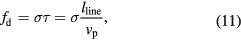
assuming that the incoming waves at all ports are zero except at port i. In contrast to conventional VNAs based on the continuous wave method, the signal frequency f is varied linearly with time in the frequency range from f0 to f1:


where σ is the ramp slope and Ts is the ramp sweep time. A single measurement channel of an FMCW VNA can be represented by the mathematical model shown in figure 1 [29]. The input signal xRF can be expressed by:


where  and
and  are the current and the initial phase of the signal, respectively. The amplitude and phase of the signal are modulated corresponding to the complex-valued transfer function H of the measurement path. The resulting signal yRF is related to one of the wave quantities (ai or bj). It is multiplied with a second input signal yLO, whose frequency is shifted by a small frequency difference fd:


Figure 1. Simplified block diagram of one measurement channel of a FMCW VNA.
Download figure:
Standard image High-resolution imageThe output signal of the multiplier contains spectral components at the sum and difference frequency. The output signal of the band-pass filter  contains only the difference frequency in the intermediate frequency (IF) band, which is constant (
 ). The filtered output signal is proportional to the real part of the complex-valued transfer function H:

The transfer function of the DUT can be obtained from the analytical signal  , which can be calculated from
  by performing a Hilbert transform:

The analytical signal of one single measurement channel is related to one of 2N wave quantities (ai or bj). Therefore, the S-parameters can be calculated by dividing the analytical signals of two measurement channels, which are related to the outcoming and the incident wave:

where the time vector t is mapped to an equivalent frequency vector  using (2).
The input signals xRF and yLO can be either generated using two synchronized synthesizers generating two frequency ramps with a small frequency difference (heterodyne principle [29]) or using one synthesizer and a delay line (metadyne principle [27]). The block diagram of one measurement channel of a metadyne FMCW VNA is shown in figure 2. The time delay τ is introduced using one or more non-dispersive (coaxial) lines resulting in a constant frequency difference
where lline and vp are the mechanical length and the wave propagation velocity of the delay line, respectively. The advantages of the metadyne principle are the lower hardware complexity of the system, since only one synthesizer is required, and the phase noise canceling at the mixer, which potentially allows for a higher measurement precision compared to heterodyne VNAs as described in section 2.2.3. However, the flexibility of the system configuration is limited since the ramp slope and length of the delay line must be chosen adequately to achieve a sufficiently high frequency difference.

Figure 2. Simplified block diagram of one measurement channel of a metadyne FMCW VNA.
Download figure:
Standard image High-resolution image2.2. Prototype design
Based on the aforementioned considerations, we developed a metadyne 3-channel prototype electronics for fast and precise 2-port reflection and transmission measurements in the frequency range from 0.5 GHz to 5.5 GHz. The major difference between the (metadyne) FMCW method and the (heterodyne) CW method regarding the hardware architecture are the signal generation and distribution. In contrast to CW systems using the stepped frequency method, where the frequency is kept constant during a measurement, a signal synthesizer used in FMCW systems must be able to generate a highly linear analog frequency ramp over the entire frequency range of interest [28]. Furthermore, the synthesizer must provide a low sideband noise (amplitude and phase noise) as well as a sufficiently high and constant output power to achieve a high measurement precision and a large DR. Due to the metadyne principle, only one synthesizer is required, which reduces the hardware complexity compared to heterodyne systems. In contrast to previously published FMCW systems [28, 29], we were able to increase the bandwidth of the signal synthesizer and all other microwave modules and significantly lower the ramp sweep time.
Furthermore, receiving channels with a low noise factor, a high compression point and a good gain flatness are required to achieve a high DR, since the DR is limited by receiver's compression point on the one hand and by noise and spurious signals on the other hand as discussed in section 2.2.3. All channels must be well isolated from each other to avoid a reduction of the spurious free dynamic range (SFDR) of the receiver and therefore the DR.
For N-port measurements the prototype electronics can be either used in conjunction with a  switching matrix as applied in this paper, or it can be extended to a full 2N-channel system due to the module-based structure. A data acquisition unit with a parallel hardware architecture is required to achieve a very low total data acquisition time in conjunction with a high precision and a high DR.
To be able to realize a hardware design at reasonable costs, an architecture with low hardware complexity was developed and all modules are based on passive microstrip circuits as well as commercially available surface mount devices. In contrast to commercial wideband VNAs, which use different microwave modules for different frequency bands [21], all modules of the FMCW prototype systems can be used over the entire frequency range of interest, which reduces the hardware complexity. In this subsection, the hardware architecture and the system's parameters are described as well as a noise analysis of the system is conducted.
2.2.1. Hardware concept.
For FMCW signal generation, we utilize our previously developed synthesizer based on fractional-N phase locked loops (PLL) [30], whose block diagram is shown in figure 3. The linear frequency ramp is synthesized in the frequency range from 8.4 GHz to 13.6 GHz ( ) and is mixed down to the desired frequency range with a constant frequency of 14 GHz (
 ). Both VCOs are stabilized and synchronized by PLLs with a common stable crystal oscillator (XCO) as reference. The signal at the mixer's output is low-pass filtered and amplified. The frequency-dependent attenuation of the microwave components is compensated by passive microstrip circuits with a high-pass like transfer function. The frequency range of the ramp synthesizer (0.4 GHz to 5.6 GHz) slightly exceeds the desired measurement frequency range to compensate for non-linear effects occurring at the upper and lower band edge, which cause a significant deviation between the actual and measured transfer function of the DUT. The synthesizer delivers a sufficiently high and constant output power around 20 dBm and the phase noise of the output signal is below −99 dBc Hz−1 at offset frequencies above 10 kHz. A detailed description of the frequency ramp generation is provided in [30].
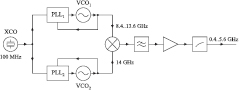
Figure 3. Simplified block diagram of the FMCW synthesizer.
Download figure:
Standard image High-resolution imageThe block diagram of the developed prototype electronics is shown in figure 4. The output of the frequency ramp synthesizer is split by a broadband 4-way multi-section Wilkinson power divider (WD). The signal xRF is coupled via a 2-way multi-section WD into the first receiving channel (R1) as well as towards the device under test (DUT) via a second 2-way multi-section WD. The reflected and transmitted waves are guided into the second (M1) and third (M2) receiving channel. The RF input signals at the mixers  ,
,  , and
, and  are related to the incident and outcoming waves a1, b1, and b2, respectively.
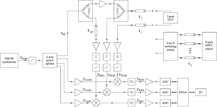
Figure 4. Simplified block diagram of the 3-channel 2-port metadyne prototype electronics, which can be utilized for N-port network analysis using a  switching matrix.
Download figure:
Standard image High-resolution imageTo avoid a degradation of the measurement precision and the DR due to poor channel isolation and the low-pass characteristic of the microwave modules, the RF and LO signals are guided towards the mixers using shielded microwave modules with a high reverse isolation ( dB), a low coupling between adjacent channels (
 dB) and a good gain flatness (
 dB). The modules consist of broadband low noise amplifiers, attenuators and passive microstrip circuits with a high-pass like transfer function. A detailed analysis of the influence of noise and spurious signals on the performance of the electronics is conducted in section 2.2.3.
Coaxial lines are inserted in front of and behind the DUT as well as in front of the first receiving channel to achieve a sufficiently high frequency difference between the input signals of the mixers:


The output signals of the mixers are low-pass filtered, amplified and analog-to-digital converted in the IF module, which consists of low noise operational amplifiers, passive filters and three 24-Bit delta-sigma analog-to-digital converters (ADC) with a sampling rate of 3.125 MSPS. The FPGA module is used for the data transfer from the ADCs to a PC. Furthermore, it potentially allows for fast multi-channel digital signal processing. However, in this work, the ADC raw data is sent to the PC, where the signal processing is performed as discussed in section 2.1. A higher order digital band-pass filter is used to suppress spectral components related to unwanted signals and broadband noise.
To achieve maximum reproducibility of the results, the signal synthesizer, the ADCs as well as the FPGA are synchronized using a common crystal oscillator as reference, i.e. all component clocks and trigger signals are derived from or are referred to the reference clock.
2.2.2. System parameter considerations.
To achieve optimum performance of the FMCW system, the system parameters must be adapted to the application and the DUT's characteristics. The selection of IF filter bandwidth BIF is a trade-off between the achievable measurement accuracy and measurement rate as well as the achievable measurement precision and dynamic range.
On the one hand, the precision and the DR of the system increase with a decreasing BIF due to decreasing integrated noise power. Therefore, BIF should be chosen as low as possible.
On the other hand, the minimum IF filter bandwidth of FMCW VNAs is not only limited by the data acquisition time, but also by the ramp slope and the transfer function characteristic of the DUT. The amplitude and phase modulation of the IF signal and the corresponding modulation bandwidth  depend on the characteristic of the transfer function of the DUT in the frequency range of interest as well as on the ramp slope. Sharp resonances in the transfer function and a high ramp slope lead to a high modulation bandwidth. Therefore, BIF must be chosen sufficiently large to avoid a degradation of the measurement accuracy.
As the modulation bandwidth is proportional to the ramp slope, an enhancement in precision and DR can only be achieved at the expense of a reduced measurement frequency range or an increased sweep time. Additionally, the length of the delay lines must be chosen adequately resulting in a sufficiently high frequency difference to avoid a degradation of precision due to increased noise at low IF frequencies.
2.2.3. Noise analysis.
The precision of the data acquisition unit can be quantified by the relative uncertainty  of the measured S-parameter, which can be defined as the ratio of the standard deviation to the mean value of the S-parameter at a certain frequency:

The relative uncertainty is the inverse of the square root of the signal-to-noise-and-spurious ratio  , which is given by:
where  ,
,  and
and  are the signal, noise, and spurious power, respectively, and
  is the frequency-dependent noise power spectral density referred to the input of the receiver. The total noise power spectral density is the superposition of the sideband noise of the synthesizer and the noise of the receiver:

For a high signal level at the receiver's input, the precision is often limited by the (integrated) sideband noise and the SFDR of the signal synthesizer. In most systems, the phase noise of the synthesizer is dominant and determines the maximum signal-to-noise-and-spurious ratio  :
:

where  is the integrated phase noise power and
  is phase noise spectral density referred to the signal power of the carrier as a function of the offset frequency
  from the center frequency of the carrier. In metadyne systems the phase noise of the down-converted signal is reduced compared to that of the input signals of the mixer, since the noise sources are correlated and the phases are subtracted (phase noise canceling). Therefore,
  can be significantly higher in metadyne systems compared to heterodyne systems. Neglecting the phase noise suppression factor and assuming a constant phase noise spectral density of
  dBc Hz−1 as well as an effective IF filter bandwidth of 10 kHz,
  can be determined to 58 dB. For a low signal level, the noise and spurious power of the receiver become dominant and
  is reduced.
The dynamic range of the data acquisition unit is the ratio of the maximum signal power at the receiver's input and the minimum detectable signal power:

The maximum signal power depends on the maximum tolerable nonlinearity of the receiving channel and is often chosen according to the 0.1 dB compression point of the microwave amplifiers and the mixer. The minimum detectable signal power is given by the receiver's input referred noise power [31]. Assuming a constant noise power spectral density of the receiver, the dynamic range is given by:
where  is the thermal noise power density and
  is the noise factor of the receiver. The noise factor of the receiver is dominated by the noise factor of the mixer and the amplitude noise of the LO signal
  , which is rectified by the mixer and thus shifted into the IF band. The amplitude noise conversion factor depends on the mixer's hardware architecture and has been determined by measurements to approximately −40 dB for the utilized double-balanced mixer (Minicircuits SYM-63LH+). The resulting noise factor of the IF channel has been determined by measurements to
  (corresponding to a noise figure of
  dB). Based on the data sheet specification of the other utilized microwave components, the noise factor of the receiver can be calculated to
  (
( dB). This results in a dynamic range of
  dB, assuming an effective IF filter bandwidth of 10 kHz.
2.3. Calibration
The accuracy of the data acquisition unit can be quantified determining the relative mean error  of the measured S-parameter, which can be defined as:

where  is the true value. The accuracy is strongly dependent on the static measurement errors introduced by the electronics and the connecting cables, which can be reduced by calibrating the system. The corresponding accuracy enhancement depends on the calibration method and the quality of the calibration standards. Furthermore, the accuracy of FMCW VNAs will be reduced if the IF filter bandwidth is chosen too low (cp. section 2.2.2).
The calibration of the system is used to reduce the static measurement errors and thus shifting the reference planes of the measurement towards the DUT. For MWI systems, the required reference planes are at the boundary or near the imaging domain, which often impedes the system calibration since not all necessary calibration standards are available. Instead of a full N-port calibration, which accounts for all systematic errors, a common approach is the normalization of the measured S-parameters [8], i.e. the measured S-parameters for the DUT are divided by the S-parameters for one calibration standard:

This reduces the number of required calibration measurements to N2, and for a reciprocal network ( ) to N + (N − 1)N/2 measurements. As calibration standards, highly reflective reference elements ('Open' or 'Short') are used for the normalization of the reflectances Sii and low-loss standards ('Thru' or 'Line') are used for the normalization of the transmittances Sji (
 ).
).
However, the achievable calibration accuracy, especially for the normalized reflectances, is often insufficient for MWI [8]. In FMCW VNAs, it is possible to separate the unwanted signal components, due to the limited isolation, directivity and matching of utilized RF modules, from the desired signals in the IF domain. This requires a sufficiently high difference in electrical length of the signal propagation paths. For example, figure 5 illustrates the different signal propagation paths of the major signal components for a reflection measurement. Due to the finite isolation of the Wilkinson divider, the RF input signal is partly coupled into the receiving channel. Furthermore, the signal guided towards to the DUT, is partly reflected at the input of the switching matrix. The unwanted signal components can be suppressed if the deviations of the frequency differences


are higher than the required IF filter bandwidth, which depends on the modulation bandwidth:


Figure 5. Different signal propagation paths of the major signal components for a reflection measurement.
Download figure:
Standard image High-resolution imageFurthermore, the calibration accuracy is limited due to multiple reflections inside the system, which result in signal contributions close to  and thus cannot be suppressed. The described method is equivalent to the time-gating technique, which is used in pulse-based systems [25], and is also applicable to CW VNAs [32], but requires a high measurement bandwidth in conjunction with a large number of frequency samples resulting in a low measurement rate.
2.4. Prototype characterization
To characterize the performance of the developed prototype electronics as well as to investigate the influence of the system parameters and the applicability of the described calibration method, we conducted measurements for different passive microwave devices and different system parameters. The measurement results are compared to those obtained with a commercial high-end CW VNA ( ZVA40). Based on the results of 100 measurements per configuration, the accuracy, the precision, and the DR of the system are calculated. The ramp sweep time and the maximum power at the receiver's input were chosen to 1 ms and −10 dBm, respectively. To investigate the influence of the ramp slope on the system's performance, measurements for two different frequency ranges (0.4 GHz to 5.6 GHz and 0.8 GHz to 3 GHz) were conducted. The corresponding frequency differences are
  kHz and
  kHz. The effective number of frequency samples can be calculated by [30]:

leading to  and
and  .
.
The IF filter bandwidth  was varied to investigate its influence on the performance parameters and it is chosen in relation to the current frequency difference:

The ZVA40 was TOSM calibrated and its input power and filter bandwidth were chosen to 0 dBm and 1 kHz, respectively. In the following subsection, the 2-port measurement results of the prototype electronics are presented. Afterwards, the influence of the switching matrix on the system's performance is investigated.
2.4.1. 2-Port measurements.
Figure 6 shows the comparison between the reflection parameter S11 for a coaxial band-pass filter as DUT measured in the frequency range from 0.5 GHz to 5.5 GHz using the prototype electronics (k = 0.3) and the ZVA40, respectively. The lower and upper cutoff frequencies of the band-pass filter are  GHz and
  GHz, respectively. The measurement results are in very good agreement with each other. The relative mean error
  of the reflection parameter measured using the prototype electronics and the ZVA40 has been calculated for OSM calibration and normalization of the reflection parameter, respectively, as depicted in figure 7. For OSM calibration, the relative mean error is between
  and
and  in the stop band of the filter and increases to 0.08 and 0.2 in the pass band of the filter. The relative error for the normalization of the reflection parameter is significantly higher compared to the OSM calibration.
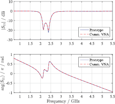
Figure 6. Scattering parameter S11 of a coaxial band-pass filter measured using the prototype electronics and a commercial VNA, respectively (OSM calibration, k = 0.3).
Download figure:
Standard image High-resolution image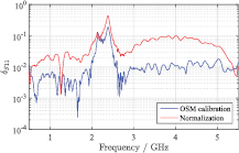
Figure 7. Relative mean error of the scattering parameter S11 of a coaxial band-pass filter measured using the prototype electronics for different calibration methods (k = 0.3).
Download figure:
Standard image High-resolution imageThe influence of the IF filter bandwidth  on the relative error of the reflection parameter S11 is illustrated in figures 8 and 9. The reduction of the filter bandwidth from k = 0.3 to k = 0.2 does not degrade the accuracy of the measurement, whereas the further reduction from k = 0.2 to k = 0.1 leads to an increase of the relative mean error, especially in the frequency range close to the sharp resonances. The major conclusion is, that the accuracy is independent of the IF filter bandwidth if
  is sufficiently high. However, if
  is chosen too low, i.e. lower than the modulation bandwidth, the accuracy will be significantly reduced as explained in section 2.2.2.

Figure 8. Scattering parameter S11 of a coaxial band-pass filter measured using the prototype electronics for different IF filter bandwidth values.
Download figure:
Standard image High-resolution image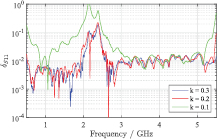
Figure 9. Relative accuracy of the scattering parameter S11 of a coaxial band-pass filter measured using the prototype electronics for different IF filter bandwidth values.
Download figure:
Standard image High-resolution imageThe measured transmission parameter for the coaxial band-pass filter is shown in figure 10. The measurement results obtained using the prototype electronics and the commercial VNA, respectively, are in good agreement overall. The amplitude and phase response ripples of the transmission parameter S21 measured using the commercial VNA are caused by static measurement errors, e.g. multiple reflections in the measurement setup, which cannot be fully suppressed due to the limited calibration accuracy. The ripple in the stop band of the filter is higher than that in the pass band, since the desired-signal-to-error-signal-power ratio is larger due to the high attenuation and the high reflection coefficients  of the DUT in the stop band. The ripple of the transmission parameter measured using the prototype electronics is significantly lower, because the signal contributions related to multiple reflections have spectral components at higher frequencies than the desired difference frequency and, therefore, are suppressed by the IF filter (cp. section 2.3).
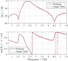
Figure 10. Scattering parameter S21 of a coaxial band-pass filter measured using the prototype electronics and a commercial VNA, respectively (normalized, k = 0.3).
Download figure:
Standard image High-resolution imageTo determine the precision and the DR of the prototype electronics, transmission measurements for different microwave attenuators with increasing attenuation have been conducted. Figures 11 and 12 show the magnitude of measured transmittance and the relative uncertainty for an effective IF bandwidth  kHz (k = 0.2), respectively. For low-loss DUTs (
 dB), the relative uncertainty of approximately
  (−65 dB) is determined by the sideband noise of the synthesizer. This corresponds to a measured signal-to-noise-and-spurious ratio for low-loss DUTs of
  65 dB. It is significantly greater than the theoretical value
  dB calculated using (18) and corresponds to an phase noise suppression factor of approximately 15 dB. The increase of the relative uncertainty at frequencies close to 0.6 GHz and 1 GHz results from spurious signals, which are generated by the synthesizer. Since the frequencies of the spurious signals are very close to the signal frequency, the spurious signals cannot be suppressed by the IF filter (in-band spurious). For high-loss DUTs, the relative uncertainty increases as the attenuation increases. The measured dynamic range of the system is approximately 80 dB, which corresponds well to the theoretical value of
  dB calculated using (20).

Figure 11. Magnitude of the scattering parameter S21 of different coaxial attenuators measured using the prototype electronics (k = 0.2).
Download figure:
Standard image High-resolution image
Figure 12. Relative uncertainty of the scattering parameter S21 of different coaxial attenuators measured using the prototype electronics (k = 0.2).
Download figure:
Standard image High-resolution imageThe relationship between the measurement precision, the DR and the IF filter bandwidth is illustrated in figure 13, comparing the relative uncertainty of the transmittance for low-loss and high-loss DUTs and two different measurement frequency ranges corresponding to different ramp slopes. For the second measurement frequency range (0.8 GHz to 3 GHz), the ramp slope and thus the frequency difference  is lower than the frequency difference
  for the frequency range from 0.4 GHz to 5.6 GHz (
 kHz,
kHz,  kHz). As k is constant (k = 0.2), the IF filter bandwidth for the second frequency range is lower:

Figure 13. Relative uncertainty of the scattering parameter S21 of two coaxial attenuators ( dB and
  dB) measured using the prototype electronics for different ramp slopes (k = 0.2).
Download figure:
Standard image High-resolution imageDue to the decreasing integrated noise, this leads to a theoretical increase of  and the DR of approximately 3.7 dB, which corresponds well to the measured increase of 3–4
  .
.
To be able to compare the DR, the maximum signal-to-noise-and-spurious ratio  (related to the precision), and the temporal resolution of the FMCW prototype electronics to those of the commercial high-end CW VNA, the DR,
  , and sweep time
  of the ZVA40 have been determined for different effective filter bandwidth values, power levels and number of frequency samples in the frequency range from 0.5 GHz to 5.5 GHz (see tables 1–3). Assuming an effective IF filter bandwidth of 60 kHz and a source power of
  dBm, the dynamic range of the prototype system is approximately 5 dB higher than that of the ZVA40 (
 dB and
  dB). The maximum signal-to-noise-and-spurious ratio of the prototype electronics is approximately 13 dB higher (
 dB and
  dB). The sweep time is significantly lower (
 ms and
  ms) for the same number of frequency sample (Z = 1180)
Table 1. Approximated average dynamic range of the ZVA40 in the frequency range from 0.5 GHz to 5.5 GHz as a function of IF filter bandwidth and input power.
 (dBm) (dBm) |
 (dB) (dB) |
 (dB) (dB) |
 (dB) (dB) |
 (dB) (dB) |
|---|---|---|---|---|
| 0 | 100 | 92 | 85 | 80 |
| −10 | 92 | 80 | 75 | 70 |
Table 2. Approximated average maximum signal-to-noise-and-spurious ratio  of the ZVA40 in the frequency range from 0.5 GHz to 5.5 GHz as a function of IF filter bandwidth and input power.
 (dBm) (dBm) |
 (dB) (dB) |
 (dB) (dB) |
 (dB) (dB) |
 (dB) (dB) |
|---|---|---|---|---|
| 0 | 70 | 63 | 58 | 55 |
| −10 | 68 | 57 | 52 | 48 |
Table 3. Approximated required sweep time of the ZVA40 without system error correction as a function of IF filter bandwidth and number of frequency samples.
 |
 (ms) (ms) |
 (ms) (ms) |
 (ms) (ms) |
 (ms) (ms) |
|---|---|---|---|---|
| 1180 | 1220 | 159 | 65 | 53 |
| 1000 | 1035 | 135 | 55 | 45 |
| 100 | 103 | 13.5 | 5.5 | 4.5 |
| 10 | 10.3 | 1.35 | 0.55 | 0.45 |
2.4.2. 2-Port measurements with switching matrix.
In this subsection, the influence of the switching matrix on the accuracy, the precision, and the DR is investigated. Figure 14 shows the comparison of the relative error of the reflectance of the coaxial band-pass filter for OSM calibration and normalization of the reflection parameter, respectively. Comparing the results in figures 14 and 7, it can be seen that the relative error for OSM calibration increases in the stop band of the filter, whereas it does not change in the pass band. For the normalized reflection parameter, the accuracy does not decrease due to the switching matrix enabling to utilize this calibration method for multi-port measurements.

Figure 14. Comparison of relative error of the scattering parameter S11 of a coaxial band-pass filter for different calibration methods measured using the 2-port prototype electronics in conjunction with the  switching matrix.
Download figure:
Standard image High-resolution imageFigure 15 shows the relative uncertainty of the transmittance for different coaxial attenuators. The minimum relative error is slightly increased to approximately  (−62 dB), while the DR is reduced to approximately 70 dB at low frequencies and 60 dB at high frequencies due to the additional insertion loss (
 dB at 1 GHz) of the switching matrix, which increases with increasing frequency.

Figure 15. Relative uncertainty of the measured scattering parameter S21 for different coaxial attenuators measured using the 2-port prototype electronics in conjunction with the  switching matrix.
Download figure:
Standard image High-resolution image3. Microwave imaging
To investigate the applicability of the proposed prototype electronics for microwave imaging, we tested it in conjunction with our previously developed 8-port MWT sensor, primarily intended for imaging of oil–gas–water flows [8]. In the following subsection, the MWT sensor and the measurement and reconstruction procedures are described. Afterwards the reconstructed permittivity distributions for different static dielectric phantoms are presented and compared to previously published results based on measurements using a commercial CW VNA.
3.1. MWT system for multiphase flow imaging
Figure 16 shows a photograph of the measurement setup for microwave imaging, which includes the proposed prototype electronics, a  switching matrix and the 8-port MWT sensor. The utilized MWT sensor consists of a metal pipe with eight wedge-shaped dielectric windows and flush-mounted rectangular waveguides. The sensor is a linear 8-port network and can be described using its scattering matrix. The electric fields of the electromagnetic waves at the interfaces between the dielectric windows and the rectangular waveguides are the input parameters of the reconstruction algorithm and can be calculated based on the measured S-parameters. In previous work [8], we utilized a commercial CW VNA in conjunction with the switching matrix limiting the temporal resolution and leading to a very low accuracy of the normalized reflection parameters Sii. Therefore, the reconstruction of the permittivity distribution was based on the normalized transmission parameters only.
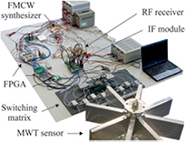
Figure 16. Photograph of the measurement setup for microwave imaging including the proposed prototype electronics, a  switching matrix and the 8-port MWT sensor.
Download figure:
Standard image High-resolution imageThe applicability of the calibration method described in section 2.3 for correction of the S-parameters of the 8-port MWT sensor was evaluated in the case that the sensor is homogeneously filled with air or polypropylene (PP), respectively. As one example, figures 17 and 18 show a comparison of the S-parameters S11 and S51 for the air-filled sensor, which were measured using the prototype electronics and the commercial VNA, respectively, in conjunction with the switching matrix, and were simulated using a 3D electromagnetic field simulation software (CST Microwave Studio ®). The measurement results using the prototype electronics and the simulation results are in good agreement, especially in the frequency range of interest from 1.2 GHz to 2.5 GHz, where the mismatch at the interface between the dielectric windows and the waveguides is low. This mismatch is neither included in the 3D simulation nor in the 2D model used for the reconstruction due to the high computational effort.

Figure 17. Comparison of the measured and simulated reflection parameter S11 of an air-filled MWT sensor.
Download figure:
Standard image High-resolution image
Figure 18. Comparison of the measured and simulated transmission parameter S51 of an air-filled MWT sensor.
Download figure:
Standard image High-resolution imageIn the frequency range of interest, the relative error  of the measured results obtained using the prototype electronics compared to the simulated results is below 0.11 for the reflection parameter and below 0.09 for the transmission parameter (see figures 19 and 20). Comparing the relative error of the measurement results obtained using the prototype electronics and the commercial VNA, it can be seen that reflection measurement accuracy for the prototype is higher by a factor of 75 (
 to
to  ), and the transmission measurement accuracy is higher by a factor of 3 (
 to
to  ). Due to the improved accuracy of the reflection parameters, the permittivity distribution can be reconstructed based on transmission and reflection results.

Figure 19. Comparison of the relative error of the reflection parameter S11 of an air-filled MWT sensor measured using the FMCW prototype electronics and a commercial CW VNA, respectively.
Download figure:
Standard image High-resolution image
Figure 20. Comparison of the relative error of the transmission parameter S51 of an air-filled MWT sensor measured using the FMCW prototype electronics and a commercial CW VNA, respectively.
Download figure:
Standard image High-resolution imageThe measurement and reconstruction procedure is described in detail in [8]. For image reconstruction the linearized one-step Gauss–Newton method [33] combined with the modified perturbation method [34] were utilized, generating a qualitative approximation of the permittivity distribution. To be able to compare the reconstruction results to those published in [8], we reconstructed the permittivity distribution for the same scenarios using air, polypropylene (PP) and tap water (TW) with the relative permittivities of  ,
,  , and
, and  , respectively.
3.2. Reconstruction results
In this subsection, the real parts of reconstructed permittivity distributions for two different inhomogeneous scenarios are presented and discussed. The reconstruction results are based on single-frequency measurement data of a broadband sweep from 0.4 GHz to 5.6 GHz of one measurement cycle. The color bar of the presented images is adapted to the reference material, i.e. the color green represents the permittivity of air ( ) or PP (
 ). Positive dielectric contrasts are indicated in red and negative contrasts in blue. The color bar is scaled to the maximum dielectric contrast of each reconstructed permittivity distribution.
Figure 21 shows the two measurement scenarios: one PP rod as well as a TW-filled polymethylmethacrylate (PMMA) tube ( ) in an air-filled sensor and a PP cylinder with one TW-filled and one air-filled drill hole, respectively. The reconstructed permittivity distribution for the first scenario based on transmission data at 1.5 GHz is shown in figure 22(a). TW appears in dark red with a estimated permittivity of
  and PP in light orange (
 ). Figure 22(b) shows the reconstructed permittivity distribution for the second scenario based on transmission data at 1.25 GHz. TW appears in dark red with an estimated permittivity of approximately
  and air in light blue (
 ).
).
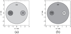
Figure 21. Measurement scenarios: (a) one TW-filled PMMA-tube at (−1.5, 0) and one PP rod at (1.5, 0) in an air-filled pipe and (b) a PP cylinder with one TW-filled drill hole at (−1.5, 0) and one air-filled drill hole at (1.5, 0).
Download figure:
Standard image High-resolution image
Figure 22. Reconstructed permittivity distribution (real part) based on transmission data measured by the proposed FMCW prototype electronics: (a) first measurement scenario at 1.5 GHz and (b) second measurement scenario at 1.25 GHz. The actual shape and position of the objects are indicated by the dashed circles.
Download figure:
Standard image High-resolution imageComparing these reconstruction results to those based on measurement data obtained with a commercial CW VNA (see figure 23), it can been seen, that the image quality in terms of the localization of the objects is higher for the FMCW measurement data due to the higher measurement accuracy. To be able to quantify the accuracy of the reconstructed center of the objects, the reconstructed permittivity along the axis of symmetry (y = 0) has been determined for both measurement scenarios as depicted in figures 25 and 26. For the first measurement scenario, the relative errors of the reconstructed x-position x0 of the objects are  and
and  for FMCW measurement data as well as
  and
and  for CW measurement data. The deviation in maximum permittivity results from the inaccuracy of the CW measurement data. For the second measurement scenario, the relative errors are
  and
and  for the FMCW data, as well as
  and
and  for the CW data.
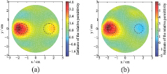
Figure 23. Reconstructed permittivity distribution (real part) based on transmission data measured using a commercial CW VNA (ZVA40): (a) first measurement scenario at 1.5 GHz and (b) second measurement scenario at 1.25 GHz. The actual shape and position of the objects are indicated by the dashed circles.
Download figure:
Standard image High-resolution image
Figure 24. Reconstructed permittivity distribution (real part) based on transmission and reflection data measured by the proposed FMCW prototype electronics: (a) first measurement scenario at 1.5 GHz and (b) second measurement scenario at 1.25 GHz. The actual shape and position of the objects are indicated by the dashed circles.
Download figure:
Standard image High-resolution image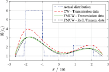
Figure 25. Real part of the reconstructed permittivity distribution along the symmetry axis (y = 0) for the first measurement scenario.
Download figure:
Standard image High-resolution image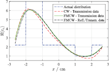
Figure 26. Real part of the reconstructed permittivity distribution along the symmetry axis (y = 0) for the second measurement scenario.
Download figure:
Standard image High-resolution image
Figure 24 shows the reconstruction results based on FMCW reflection and transmission data. Compared to the results based on FMCW transmission data only, the centers of the dielectric phantoms are shifted towards the center of the imaging domain, which corresponds to an improved accuracy of the reconstructed distributions. The relative errors are  and
and  for the first measurement scenario, as well as
  and
and  for the second scenario.
It can be concluded, that the improved accuracy of the scattering parameters measured using the FMCW prototype electronics results in an enhanced accuracy of the images based on transmission data. The additional utilization of reflection data for the reconstruction leads to a further improvement in image accuracy.
4. Discussion
In this work, we presented a data acquisition unit based on the FMCW method intended for broadband MWI systems. The proposed metadyne prototype electronics allows for very fast broadband scattering parameter measurements without compromising the measurement precision and the DR as expected from the description in [27]. For a constant number of frequency samples (Z = 1180), the dynamic range of the developed prototype electronics and the commercial high-end CW VNA are approximately equal (80 dB at 50 kHz IF filter bandwidth), whereas the precision of the prototype is higher (65 dB compared to 52 dB) and the sweep time of the prototype is significantly shorter (1 ms compared to 65 ms).
The main advantages and limitations of the proposed metadyne FMCW system compared to a (commercial) CW heterodyne VNA are as follows. Firstly, the settling time at each frequency point related to the stepped frequency data acquisition procedure are avoided by modulating the frequency linearly, which allows for a significantly lower data acquisition time for a high number of required frequency samples. Secondly, the phase noise of the IF signal can be reduced (phase noise canceling) leading to an increased maximum signal-to-noise-and-spurious ratio and thus to an increased measurement precision (cp. section 2.2.3). The measured phase noise suppression factor is approximately 15 dB (cp. section 2.4.1). Thirdly, systematic measurement errors can be easily reduced by digital filtering of the IF signal (cp. section 2.3), which is particularly advantageous for MWI systems as described and demonstrated in section 3.1. Fourthly, the hardware complexity is significantly lower, since only one synthesizer is required. Fifthly, the FMCW method is particularly advantegeous compared to CW network analysis for a large number of frequency samples. As the number of required samples decreases, the deviation in terms of data acquisition time decrease (cp. table 3 in section 2.4.1). Lastly, the flexibility of the system configuration is limited since the ramp slope and mechanical length of the delay line must be chosen adequately to achieve a sufficiently high frequency of the IF signal.
In contrast to previously published systems for FMCW based network analysis [28, 29], the measurement bandwidth of the prototype electronics is higher and sweep time is significantly lower (1 ms compared to 20 ms). The achieved precision, accuracy, and dynamic range cannot be easily compared since these parameters are not quantified in the literature. However, based on the presented graphs in [28, 29], it can be concluded that the performance parameters of the proposed prototype electronics are at least as good as those of the previously published systems despite the significantly lower sweep time.
The influence of the system parameters on the accuracy, precision, and dynamic range have been described and validated by measurements. Further improvements in terms of precision and dynamic range are possible by reducing the in-band spurious and the amplitude noise of the synthesizer and utilizing a triple-balanced mixer in the receiver for an increased 0.1 dB compression point.
5. Conclusion
In this paper, we presented a data acquisition unit for fast and precise S-parameter measurements, which is a major challenge designing MWI systems. The proposed metadyne 2-port prototype electronics based on the FMCW approach allows for reflection and transmission measurements in the frequency range from 0.5 GHz to 5.5 GHz with a signal-to-noise-and-spurious ratio of 65 dB and a DR of 80 dB. The sweep time (1 ms) is significantly shorter than the data acquisition time of commercial VNAs (65 ms) and that of previously published FMCW systems (20 ms), potentially allowing for fast broadband microwave imaging. The applicability of the prototype electronics and the presented calibration technique for microwave imaging has been validated using an 8-port MWT sensor and a switching matrix. The accuracy of the reconstruction results for different static imaging scenarios has been improved compared to previously published results. The advantages and limitations of the metadyne FMCW technique compared to the heterodyne CW technique have been discussed. It can be concluded that the presented data acquisition unit is well-suited for broadband MWI systems requiring a high measurement rate in conjunction with a high number of frequency samples as well as a high measurement precision and a high DR. For applications requiring a very low total data acquisition time, the 2-port prototype electronics can be easily extended to a full N-port system.