
Abstract
Direct-band-gap Germanium-Tin alloys (Ge1-xSnx) with high carrier mobilities are promising materials for nano- and optoelectronics. The concentration of open volume defects in the alloy, such as Sn and Ge vacancies, influences the final device performance. In this article, we present an evaluation of the point defects in molecular-beam-epitaxy grown Ge1-xSnx films treated by post-growth nanosecond-range pulsed laser melting (PLM). Doppler broadening – variable energy positron annihilation spectroscopy and variable energy positron annihilation lifetime spectroscopy are used to investigate the defect nanostructure in the Ge1-xSnx films exposed to increasing laser energy density. The experimental results, supported with ATomic SUPerposition calculations, evidence that after PLM, the average size of the open volume defects increases, which represents a raise in concentration of vacancy agglomerations, but the overall defect density is reduced as a function of the PLM fluence. At the same time, the positron annihilation spectroscopy analysis provides information about dislocations and Ge vacancies decorated by Sn atoms. Moreover, it is shown that the PLM reduces the strain in the layer, while dislocations are responsible for trapping of Sn and formation of small Sn-rich-clusters.
Export citation and abstract BibTeX RIS

Original content from this work may be used under the terms of the Creative Commons Attribution 4.0 license. Any further distribution of this work must maintain attribution to the author(s) and the title of the work, journal citation and DOI.
1. Introduction
In optoelectronics, the integration of silicon-compatible direct-band-gap materials into the complementary metal-oxide-semiconductors technology would allow to fabricate lasers and optical interconnectors. Ge1-x Snx alloys are among the most promising materials to replace Si in future optoelectronics. These alloys enable an effective band gap engineering due to (i) alloying the indirect semiconductor Ge with the negative direct-band-gap material Sn [1, 2]; (ii) strong n-type doping [3–5] or (iii) strain engineering [6, 7]. The conversion from an indirect- to a direct-band-gap material was experimentally shown on partly strain-strain relaxed Ge0.9Sn0.1 by Ghetmiri et al [8]. Unfortunately, the solid solubility of Sn in Ge in thermodynamic equilibrium is below 1.1 at. % [9] and compressive strain shifts the direct-band-gap transition to higher Sn concentrations [2]. This means that the fabrication of direct-band-gap Ge1-x Snx alloys requires highly non-equilibrium processing techniques and methods to release the in-plane compressive strain. Currently, the main fabrication techniques for Ge1-x Snx alloys are molecular beam epitaxy (MBE) [10–12] and chemical vapor deposition [1, 13]. In order to avoid Sn segregation, the growth of the alloy is performed with high growth rates and at temperatures normally between 25 [14, 15] and 390 °C [16–18], depending on the desired Sn concentration and growth method. This non-equilibrium growth causes the formation of different types of defects [16]. Stain relaxation can be achieved in multiple ways: (i) using buffer layers with a lattice parameter in the range of the targeted Ge1-x Snx alloy; (ii) the formation of misfit or threading dislocations due to the growth of layers thicker than the critical thickness for pseudomorphic growth [19, 20]; (iii) alloy engineering by adding smaller elements into the Ge1-x Snx alloy system, e.g. Si [21], P [6], or B [11]; (iv) using post-growth thermal treatment [7]; (v) strain release by the fabrication of nano-structures [1, 22, 23]. In recent years, first success could be achieved by improving the growth process and using methods to gain partly strain-relaxed Ge1-x Snx alloys. Wirths et al [2] presented the first Ge1-x Snx -based laser, where lasing was observed up to 100 K from a sample containing 12.6% of Sn. Shortly after that, Chrétien et al [23] demonstrated compressively strained Fabry-Pérot Ge0.84Sn0.16 micro-lasers with lasing action persisting up to 273 K [23]. In general, the quality of the optically active layer mainly determines the laser performance and reliability, which depends on the presence of point defects like vacancies.
Recently, first results based on post-growth pulsed laser melting (PLM) on Ge1-x Snx alloys with a promising in-plane strain relaxation effect were published [7, 24]. The implementation of strain-relaxed PLM Ge1-x Snx as a virtual substrate could be a helpful approach for further improvements. However, the understanding of the mechanisms of defect formation in Ge1-x Snx alloys after PLM and their function in the system is crucial for the successful integration of Ge1-x Snx alloys within the Si technology. Positron annihilation lifetime spectroscopy (PALS) is one of the most sensitive techniques to investigate open volume defects like Sn and Ge vacancies [16]. PALS offers the possibility to probe single vacancies (one missing atom). In addition, variable energy PALS (VE-PALS) allows studying the depth distribution of vacancies in the matrix [4].
In this paper, we study the evolution of open volume defects like Sn and Ge vacancies in MBE-grown Ge1-x Snx alloys after strain engineering by post-growth PLM. VE-PALS suggests the reduction of the concentration of mono-vacancy-Sn complexes and the average size of big vacancy clusters in the molten layer. Transmission electron microscopy (TEM) results show the formation of Sn-rich Ge1-x Snx filaments. The strain transition from compressive to tensile is confirmed by micro-Raman (μ-Raman) spectroscopy and discussed in detail in [7]. The presented post-growth PLM may be applied for the fabrication of strain-relaxed or even tensile-strained virtual substrates for the growth of strain-free Ge1-x Snx layers.
2. Experimental part
2.1. Material fabrication
A 290 nm-thick Ge0.89Sn0.11 layer was epitaxially grown by MBE on a (100)-oriented 4 inch p-type Si substrate with a sheet resistance of Rs = 10–20 Ω cm. The entire layer stack is shown in figure 1(a), and a detailed description of the process flow can be found elsewhere [7]. Before the growth of the Ge0.89Sn0.11 layer, we grew a 50 nm-thick Si virtual substrate followed by a 100 nm-thick Ge virtual substrate and a 300 nm-thick Ge-buffer layer and performed an in-situ post-growth thermal treatment at 750 °C for 5 min. Afterwards, the 290 nm-thick Ge0.89Sn0.11 film was grown at 120 °C. The post-growth strain and defect engineering was performed by PLM using a XeCl excimer laser with a wavelength of 308 nm, a pulse length of 28 ns, and an energy density varying from 0.15 to 0.5 J cm−2. The effective annealing area was 5 × 5 mm2, as visualized schematically in figure 1(c).

Figure 1. Process flow and schematic of the layer stack cross-section of the Ge0.89Sn0.11 material grown on Si by MBE before (a) and after post-growth nanosecond-range PLM with energy densities above the melting threshold (b). Schematic of the post-growth PLM process (c).
Download figure:
Standard image High-resolution image2.2. Characterization of materials
The influence of the PLM process on the microstructural and electrical properties of the Ge1-x Snx alloys as well as on the defects within them was studied using µ-Raman spectroscopy, TEM, Doppler broadening—variable energy positron annihilation spectroscopy (DB-VEPAS) and VE-PALS, and Hall-effect measurements.
µ-Raman spectroscopy was performed on a Horiba LabRam n°1/24 h system equipped with a Nd:YAG laser with a wavelength of 532 nm and a liquid-nitrogen-cooled CCD camera. All measurements were performed in backscattering geometry with a laser power of 1 mW focused on a circular area with 1 µm diameter. The phonon spectra were recorded in the wavenumber range of 50–550 cm−1. The penetration depth of the green laser (532 nm) in Ge is approximately 20 nm from the surface [25].
TEM investigations of the as-grown and pulsed-laser-molten samples were done in cross-sectional geometry using a Titan 80–300 microscope (FEI) operated at an accelerating voltage of 300 kV. High-angle annular dark-field scanning transmission electron microscopy imaging and spectrum imaging analysis based on energy-dispersive x-ray spectroscopy (EDXS) were performed at 200 kV with a Talos F200X microscope equipped with a Super-X EDX detector system (FEI). Prior to (S)TEM analysis, the specimen mounted in a high-visibility low-background holder was placed for 10 s into a Model 1020 Plasma Cleaner (Fischione) to remove potential contamination. To record the bright-field TEM images, the TEM specimen was oriented in Si [ ] zone axis geometry relative to the electron beam.
The type of defects and their concentration and depth distribution in the Ge1-xSnx alloys were investigated by DB-VEPAS and VE-PALS. DB-VEPAS measurements were conducted at an apparatus for in-situ defect analysis [26] of the slow positron beamline (SPONSOR) [27]. Implanted into a solid material, positrons thermalize and shortly diffuse until they finally annihilate with electrons in delocalized lattice sites (interstitials) or localize in vacancy-like defects and interfaces. As a consequence of annihilation, two anti-collinear 511 keV gamma photons are emitted. Since at the annihilation site thermalized positrons have very small momentum compared to the electrons, a broadening of the 511 keV line is observed mostly due to the momentum of the electrons, which is then measured with a high-purity Ge detector (overall energy resolution of 1.09 ± 0.01 keV at 511 keV). This broadening is characterized by two distinct parameters, S and W, defined as fractions of the annihilation line in the middle (511 ± 0.74 keV) and outer regions (508.7 ± 0.30 keV and 513.30 ± 0.30 keV), respectively. The S-parameter is the fraction of positrons annihilated with low momentum valence electrons and represents vacancy-type defects and their concentration. The W-parameter approximates the overlap of the positron wave function with the high-momentum core electrons, enabling the direct analysis of defect atomic decoration. Plotting S as a function of the positron implantation energy, Ep , provides depth-dependent information of the defect density, whereas S–W plots are used to examine the atomic surrounding of the defect site and its size (type) [28].
The positron lifetime experiments were performed at the mono-energetic positron spectroscopy beamline of the radiation source ELBE (Electron Linac for beams with high Brilliance and low Emittance) at Helmholtz-Zentrum Dresden-Rossendorf (Germany) [29]. Similarly to DB-VEPAS, positrons were accelerated and monoenergetically implanted into samples in the range between Ep = 1–10 keV (Ep = 0.05–35 keV for DB-VEPAS), which realizes depth profiling. A mean positron implantation depth was approximated using a simple material density ρ dependent equation (1) [30],
<z> is an approximation of the depth and cannot be treated as an absolute measure, since it does not account for positron diffusion. However, it gives a reliable depth estimation for materials with large defect concentration, hence low positron diffusion length. A digital lifetime CrBr3 scintillator detector operated by a homemade software, utilizing a SPDevices ADQ14DC-2X digitizer with 14-bit vertical resolution and 2 GS s−1 horizontal resolution, was used (the overall time resolution was about 230 ps) [31]. The resolution function required for spectrum analysis was composed of two Gaussian functions with distinct intensities depending on the positron implantation energy, Ep , and appropriate relative shifts. All spectra contain at least 5 × 10⁶ counts. The lifetime spectra were analyzed as a sum of time-dependent exponential decays according to equation (2), convoluted with the spectrometer timing resolution [32] using a nonlinear least square approach provided by the PALSfit fitting software [33],
The indices i correspond to the number of discrete lifetime components (defect sizes, types) in the spectra with individual lifetimes τi and their relative intensities Ii . A commercial undoped bulk Ge substrate was used as reference for DB-VEPAS and VE-PALS.
The Hall-effect measurements in van-der-Pauw configuration were performed using a HMS 9709 A measuring system from LakeShore. Close to the sample corners, 100 nm-thick circularly shaped Au contacts with a diameter of 3 mm were fabricated by thermal evaporation. The magnetic field was varied between −5 and 5 T.
3. Results and discussion
3.1. Microstructural investigation
Micro-Raman spectroscopy is used as a fast selection method to observe the PLM-initiated strain relaxation mechanism in Ge0.89Sn0.11 reported in our previous work [7]. Figure 2 shows the µ-Raman spectra obtained from samples before and after PLM with energy densities varying from 0.15 to 0.5 J cm−2. The Ge–Ge phonon mode in strain-free Ge are located at 300.5 ± 0.1 cm−1 [34]. The peak position of the phonon mode in Ge can be shifted to lower or higher wavenumbers due to different phenomena like strain, alloying, disorder, or by phonon-plasmon interaction in heavily doped semiconductors. In general, compressive strain shifts the phonon mode to higher wavenumbers, while tensile strain causes a red shift [7, 35]. Alloying Ge with heavier elements like Sn shifts the phonon mode to lower wavenumbers [36]. Therefore, µ-Raman spectroscopy is a contactless and non-destructive method to investigate the changes in composition and strain in solids. Analyzing the phonon spectra, the coexistence of different phenomena that can compensate the changes by each other has to be taken into account. On the one hand, the pseudomorphic growth of Ge0.89Sn0.11 on Ge by MBE causes in-plane biaxial compressive strain. Therefore, the peak position of the as-grown Ge0.89Sn0.11 layer is located at 296.6 cm−1, instead of 291.3 cm−1 according to the theoretical calculation (see the vertical dashed line in figure 2). On the other hand, PLM may lead to a redistribution of Sn and strain relaxation, as discussed in detail in [7]. The PLM process causes strain relaxation in the top part of the Ge1-x Snx layer, which can be observed by the shift of the phonon mode towards a lower wavenumber. The sample annealed with 0.15 J cm−2 is not affected by the pulsed laser, since the peak position coincides with the as-grown state. Annealing with 0.2 J cm−2 shows a slight red shift because the laser energy is close to the melting threshold. All other samples annealed with a pulsed laser energy density higher than 0.2 J cm−2 show the main phonon mode at about 291 ± 1 cm−1, which is close to the theoretical peak position of strain-relaxed Ge0.89Sn0.11. Furthermore, a reduced Ge–Ge vibrational mode width can be observed after PLM for energy densities >0.15 J cm−2. This can be attributed to a thermally activated rearrangement of Ge atoms in the lattice and the strain relaxation. Furthermore, a reduction in the width of the Ge–Ge vibrational mode was observed after PLM at energy densities >0.15 J cm−2 in figure 2. This can be attributed to a rearrangement of Ge atoms in the Ge1-x Snx lattice and strain relaxation.
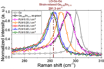
Figure 2. Normalized µ-Raman spectra for the Ge–Ge longitudinal optical phonon mode of the as-grown Ge0.89Sn0.11 and PLM-treated Ge1-x Snx alloys with energy densities of 0.15, 0.20, 0.30, 0.40, and 0.50 J cm−2. The resolution of the peak position is ± 0.1 cm−1.
Download figure:
Standard image High-resolution imageThe microstructure and element composition of the as-grown and PLM-treated samples were investigated using cross-sectional TEM-based analyses. In particular, figures 3(a) and (b) show superimposed Si, Ge, and Sn element distribution maps obtained from the upper part of the layer stack. The general setup matches the schematic presented in figures 1(a) and (b). Figures 3(c) and (d) show the bright-field TEM images recorded from the areas marked with the white-dashed squares in figures 3(a) and (b), respectively. In the as-grown state, about 80 nm above the Ge1- x Snx /Ge interface, first vertical structures with a columnar signature appear (see figures 3(a) and (c)). Line scan analyses, presented in figures 3(e) and (f), confirm that the columnar structure, which could be caused by small process instabilities during MBE growth, is related to a slightly varying Sn concentration.
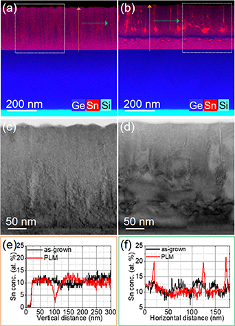
Figure 3. Cross-sectional TEM-based analysis of the as-grown sample ((a), (c), and (e)), and after PLM treatment with an energy density of 0.5 J cm−2 ((b), (d), and (f)). Panels (a) and (b) show representative superimposed Ge (blue), Sn (red), and Si (cyan) EDXS-based element distributions, while (c) and (d) present the bright-field TEM images of the regions marked with white-dashed squares in (a) and (b), respectively. The diagrams in (e) and (f) depict the vertical and horizontal line scans, indicated in (a) and (b) with orange and green arrows, respectively.
Download figure:
Standard image High-resolution imageAfter PLM, the Ge1-x Snx surface is rearranged and larger defect structures are visible between the Ge1- x Snx /Ge interface up to about 100 nm below the Ge1-x Snx top surface (see figures 3(b) and (d)). The presence of these defect structures is not surprising since the strain relaxation comes with the formation of misfit dislocation networks and threading dislocations. According to the EDXS analysis (figure 3(b)), there is a Sn-depleted region between the near-surface molten and near-substrate non-molten zone, which is visible in figure 3(e) as a sharp dip in the vertical Sn profile of the PLM-treated sample. Below the Sn-depleted zone, we find a Ge0.89Sn0.11 layer with a microstructure similar to the as-grown state. Above the Sn-depleted zone, there are Sn-rich clusters and filaments in a Ge0.90Sn0.10 matrix. The filaments are well visible as sharp peaks in the horizontal Sn profile in figure 3(f). Similar filament structures were discussed by Narayan [37] for highly doped Si after PLM. He concluded, if the non-equilibrium solubility of the alloy exceeds a certain value, the solid-liquid interface becomes unstable and the structure experiences a cellular breakdown during the ultra-fast solidification. However, there are some reasons against this theory, as discussed in [24]. The Sn-rich filaments in the present study are still part of the Ge1-x Snx crystal structure [7]. Assuming, the filaments might be an early stage of phase separation, there should be a significant increase of the Sn concentration towards the surface, which is not visible in figure 3(b). Abdi et al reported similar Sn-rich Ge1-x Snx filaments in Ge0.89Sn0.11 with an enhanced defect concentration and explained that a combination of pipe diffusion and spinodal decomposition might be the origin of the filaments [24]. In fact, our filaments also contain some defect structures. On the other hand, the columnar fluctuation in the Sn concentration of the as-grown state might promote the filament formation after PLM. Apart from the filaments, the microstructure of the Ge0.90Sn0.10 matrix close to the sample surface seems to be homogenous and comparable with the as-grown state [7].
3.2. Defect analysis
The influence of PLM on the defect concentration, defect depth distribution and electrical properties was examined by DB-VEPAS, VE-PALS and Hall-effect measurements.
The relative changes of defect density (the S-parameter) and elemental decoration of defects (the W-parameter) across the sample thickness were studied by DB-VEPAS (see figure 4 and supplementary figure S 1). In general, the plotted annihilation line parameter S in figure 4(a) is directly proportional to the defect concentration. However, it depends on the defect size and tends to saturate for larger defect concentrations. We observe an increase of S as a function of PLM energy density applied on the film as well as a variation of the maximum S (Ep) position reflecting changes across the Ge1-x Snx layer thickness. This observation correlates with the higher amount of defects between 50 and 200 nm in the PLM 0.5 J cm−2 sample (see figure 3(d)). The concentration of open volume defects is higher compared to the as-grown state (lower slope and a maximum at Ep = 7 keV) and a Ge-reference sample (lowest slope, no maximum). Interestingly the S-parameter at Ep = 0.05 keV is for all PLM samples very similar as visible in figure 4(a) and table 1. Similar surface properties were also indicated by µ-Raman results in figure 2. The W-parameter can be used to evaluate atomic environment at the positron annihilation site and is presented in figure S 1. At Ep = 10 keV we have a peak, which can be allocated to the Ge0.9Sn0.1/Ge interface because W of the Ge0.89Sn0.11 approaches the W value of Ge-reference sample. For the PLM samples, we have additionally the Sn depletion region between the PLM affected Ge1-x Snx and unaffected Ge0.89Sn0.11 layer (see figure 3(b)), which is however not clearly visible from positron annihilation spectroscopy (PAS) in figure S 1(b)). It is likely due to the fact that the Sn depleted layer is too thin and deeply buried for positrons to resolve it. In order to compare changes in defect density (S) and changes in the defect decoration types (W), we plotted both in figure 4(b) at two characteristic depths of each sample. The discussed depth are (i) lower depth corresponding to the S (Ep ) maximum (indicated by the arrow in figure 4(a)) and (ii) the deeper depth—W (Ep ≈ 10 keV) (see figure S 1(b)). The data points from the lower depth exhibit a linear relation to each other, which indicates that they share a similar defect type as the reference sample. Deeper in the film a trend in direction towards the Ge reference sample is found. Hence, the observed change at Ep ≈ 10 keV is related to the increased defect decoration by Ge (less decoration of Sn). Moreover, for both considered depths the local stoichiometry must contain Sn atoms as no obvious linear relation can be drawn between Ge reference and Ge1-x Snx data points.
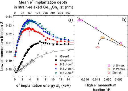
Figure 4. Annihilation line parameter S of the Ge-reference, as-grown Ge0.89Sn0.11 and after PLM with an energy density of 0.3, 0.4, and 0.5 J cm−2 (a) as a function of positron implantation energy Ep and mean positron implantation depth <z> with corresponding fits. (b) S–W plot of the maximum values from S (Ep ≈ 4 or 7 keV) and W (Ep ≈ 10 keV) dependencies compared to the bulk value (Ep = 35 keV) for Ge reference sample.
Download figure:
Standard image High-resolution imageTable 1. The calculated Ssurf, S1, thickness d1, effective diffusion length L+,1, and defect concentration cν for the germanium reference sample, Ge0.89Sn0.11 as-grown state and Ge1-xSnx samples after PLM with 0.3, 0.4 and 0.5 J cm−2, respectively, were calculated with VEPFit code [38]. In brackets a standard deviation for the last digit after comma is shown. Ssurf was calculated close to the sample surface at (Ep = 0.05 keV).
| Sample name | Ssurf | S1 | d1 (nm) | L+, 1 (nm) | cν (×10−5 atom−1) |
|---|---|---|---|---|---|
| Ge-ref | 0.4770(2) | 0.5048(3) | — | 111 ± 3 | <1 |
| GeSnas-grown | 0.475(2) | 0.514(2) | 290 | 37 ± 3 | 3.5 ± 0.3 |
| GeSnPLM-0.3 | 0.499(3) | 0.528(1) | 100 | 10 ± 2 | 54 ± 11 |
| GeSnPLM-0.4 | 0.506(4) | 0.538(1) | 140 | 14 ± 2 | 27 ± 4 |
| GeSnPLM-0.5 | 0.506(3) | 0.538(1) | 195 | 18 ± 3 | 16 ± 3 |
The VEPFit code [38] has been utilized for the analysis of positron diffusion length L+, which is inversely proportional to defect concentration cv . The code enables evaluation of defect densities as a function of depth in multilayer systems. The S (Ep) curves in figure 4(a) were fitted assuming a four-layer system by using the layer stack presented in figure 1 consisting of the strain-relaxed Ge1-x Snx (including Sn depleted Ge1-x Snx ), unaffected Ge0.89Sn0.11, Ge, and Si substrate. The selected parameter and calculation results are summarized in table 1. The layer thickness d1 of Ge1-x Snx and Ge0.9Sn0.1 was determined by RBS and TEM as explained in [7]. and was fixed to these values for the calculation. The density of the strained Ge0.89Sn0.11 and strain-relaxed Ge1-x Snx layers were determined by HRXRD and RSM results (see [7] and appendix D) to ρGe0.89Sn0.11 = 5.14 g cm−3 and ρGe1-x Snx = 5.11 g cm−3, respectively. For Ge (ρGe = 5.32 g cm−3 [39]) and Si (ρSi = 2.33 g cm−3 [40]) literature densities were used. L+ for the Ge-buffer layer and Si-substrate was fixed to 111 nm and 220 nm, respectively, based on the Ge single crystal substrate measurement and literature [41]. The boundary between the Ge-buffer layer and the substrate was kept constant at depth of 700 nm, according to planned deposition conditions. For simplicity 15 nm was added to d1 in case of PLM samples to account for the thickness of depleted layer. Such a thin layer has negligible influence on the positron annihilation as no clear variation of the S (Ep) curve shape has been isolated across the depth. According to the fitting results the calculated positron diffusion lengths of the PLM treated films are too short for positrons to directly arrive to the depleted layer, hence the defect density in the Sn depleted layer must be similar to the PLM treated Ge1-x Snx top or the Ge0.89Sn0.11 bottom layers. d1 for the as-grown Ge0.89Sn0.11 was fixed to 290 nm and the obtained L+,1 = 37.4 nm served as a reference for the unaffected Ge0.89Sn0.11 layer in the PLM treated samples (see figure 1(b)). Hence, the only free fitting parameter was the effective diffusion length in the top layer L+,1 .
The calculated defect concentration (∼3.5 × 10⁻⁵ atom−1) of the as-grown sample is relatively low due to a large L+, 1 = 37 ± 3 nm, but is still three times larger than the undoped Ge-reference crystal. The slight loss of crystal coherency compared to Ge-reference is not surprising for materials deposited by MBE, since surface defects in the buffer or strain relaxation events in Ge0.89Sn0.11 layer can lead to defects at the interface. After PLM with 0.3 J cm−2, when the molten layer is about 100 nm, the defect concentration increases about 15 times. This suggest that the presented strain relaxation events leads to an abrupt formation of open volume defects. By increasing the PLM energy densities to 0.4 J cm−2 and 0.5 J cm−2, the defect concentration cν drops down due to annealing effects. Although on the first glance, a general increasing trend of the calculated S as a function of PLM energy density seems contradicting the drop of defect concentration, as we will show later, the raising density of larger vacancy clusters (see figure 5(c)) is likely the main cause of the S-parameter increase. This indicates that the high diffusion coefficient in the molten film may be also in combination with the assumed pipe diffusion mechanism reported by Abdi et al can be an effective way for strain relaxation and open volume accumulation [24].

Figure 5. Average positron annihilation lifetime τav of the samples in the as-grown state and after PLM with an energy density of 0.4 J cm−2 and 0.5 J cm−2 as a function of positron implantation energy Ep and mean positron implantation depth <z> (a). Discrete positron lifetime components τ1 (closed symbols) and τ2 (open symbols) obtained by spectra decomposition of τav (b). Relative intensities I1 and I2 of the components τ1 and τ2 (c). ATSUP calculations of positron lifetime as a function of lattice parameter a for bulk Ge0.9Sn0.1 and VGe configurations (d), a number of Sn nearest-neighbors (≤4) and next-nearest-neighbors donors decorating Ge atom and VGe in Ge0.9Sn0.1 (e), and in function of vacancy agglomeration size for a Ge and Ge0.89Sn0.11 crystals (f). The calculated lifetimes from (f) of bulk Ge0.9Sn0.1 and vacancy cluser sizes with 3 (V3) and 4 (V4) vacancies are highlighted in green in (b).
Download figure:
Standard image High-resolution image
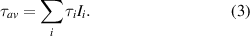
In addition, we have studied the defect depth distribution in the as-grown and annealed samples using VE-PALS. Figure 5(a) shows the depth change of the average positron annihilation lifetime τav , which is the weighted average defect size across sample thickness. τav can be expressed by equation (3). The positron annihilation lifetime τi refers to the characteristic annihilation sites (vacancy like defects of different sizes) and Ii is the relative number of positrons trapped at these defect types. In the other words τav indicates the density of vacancy like (open volume) defects,
In general, the positron lifetime increases with increasing the size of the open volume defects and negativity of the defect charging state (more negative—slightly longer lifetime) [42]. In figure 5(a) we obtain for τav at 3 keV (∼42 nm) an increases from ∼275 ps in the as-grown sample to about ∼293 ps and ∼284 ps in the sample annealed with the pulsed laser energy densities of 0.4 J cm−2 and 0.5 J cm−2, respectively. This is caused by an increase of the average size of defects after PLM compared to the as-grown state. For the positron implantation energies lower than 2 keV, all curves in figure 5(a) show a longer lifetime (close to the sample surface) because the signal is superimposed by the surface and its defect states [43–45]. For higher positron implantation energies, only the defect states are visible (the most pure defect contributions can be obtained at the S-parameter maximum in figure 4(a).
From equation (3) we see that τav is a combination of the discrete positron lifetime components τi (τ1 and τ2), obtained by the spectra decomposition (figure 5(b)) and their relative intensities I1 and I2 (figure 5(c)). In general, positron lifetime scales with the local electron density, which is influenced by the size of open volume defects and their chemical composition, carrier concentration, and the defect charge state [42]. In our case τ1 is not a straight forward to define as it could represent a defect free GeSn material (bulk annihilation in figure 5(b)), a fully Sn-decorated Ge-mono-vacancy (VGe + nSnGe, where n is the number of Sn atoms substituting Ge) or GeSn with shallow trapping dislocations [46]. On the other hand, τ2 describes vacancy agglomerations (clusters containing certain number of vacancies). The positron lifetime components τ1 and τ2 as a function of depth reveal a defect size evolution due to annealing (see figure 5(b)). The first lifetime component τ1 increases by not more than ∼16 ps across the depth after PLM with 0.4 J cm−2 which is followed by a τ1 drop after PLM with 0.5 J cm−2. It is accompanied by a reduction of its relative intensity I1 by not more than ∼10% and indicates overall reduction of positron annihilation with defect states related to τ1. To understand the change of τ1, the so-called atomic superposition (ATSUP) [47] calculations were performed for Ge (see table S I) and a Ge0.9Sn0.1 cubic crystals. Here we used Ge0.9Sn0.1 because the Ge1-x Snx the cross-section TEM line scan presented in figure 3(f) shows that Sn concentration in the matrix between filaments in the PLM treated sample is lower than that in the as-grown sample. The same was concluded from XRD data [7].
The calculated positron lifetime as a function of the lattice parameter and the number of Sn atoms decorating VGe are presented in the tables S II and S III and plotted in figures 5(d)–(f), respectively. The details about our simulations and the calculation results can be found in the supplementary materials sections B and C.
From the ATSUP calculation we obtain that the calculated lifetime in Ge0.89Sn0.11 is increasing with the lattice parameter for both bulk and VGe (see figure 5(d)), as expected. The numbers of Sn substitutions of Ge in Ge0.9Sn0.1 has only a minor influence on the positron lifetime for bulk, but a substantial reduction is observed for VGe (figure 5(e)). Finally, positron lifetime scales with the vacancy cluster size in a similar way for Ge0.9Sn0.1 as for Ge (figure 5(f)). With this results we reveal that the change of τ1 is likely a superposition of lattice parameter variation (figure 5(d)) and a change of the Sn distribution at VGe (figure 5(e)). Therefore, the component τ1 combines the positron annihilation in bulk and at the Sn-decorated VGe. Experimentally, the reference lifetime in bulk Ge is in the range of 224–228 ps [48] and decreases with increasing Sn concentration [16], which is in line with our calculations. Moreover, we assume that the average area of filaments i.e. regions with high Sn content (equivalent to the shorter positron lifetime due to larger Sn decoration of VGe) increases with PLM energy. They are not observed in the as-grown sample at all. There the positron lifetime is the shortest and likely represents bulk annihilation. The slight variation of lifetime between different PLM energy densities, on the other hand, is likely related to a variation of the average number of Sn atoms bonded with VGe existing at the direct interface with filaments and the Ge1-xSnx matrix in between.
Further, the relative intensity I1 decreases after the PLM (see figure 5(c)), which reflects the overall reduction of the Sn-vacancy complex concentration. In general, after PLM τ2 is reduced in all samples. This means that the average size of larger vacancy clusters decreases, but simultaneously the relative intensity I2 increases (see figure 5(c)), indicating larger fraction of positrons annihilating with vacancy agglomerations modified due to PLM. The τ2 is in the order of 400 ps referring to the vacancy clusters with about three to four agglomerated vacancies (see figure 5(b) and table S III). Larger concentration of vacancy clusters can increase scattering and reduce the mobility of charge carriers as shown by the Hall effect measurements [49].
The results of the Hall-effect measurement are summarized in table 2. The hole concentration in the as-grown state is 3.3 × 1018 cm−3 at 300 K because of unintentional p-type doping during the growing process of Ge1-x Snx . This background doping is already one magnitude higher than indicated in earlier reports [50]. After PLM, the hole concentration is increased to 4.1 × 1018 cm−3 (0.4 J cm−2) and 4.9 × 1018 cm−3 (0.5 J cm−2) at 300 K. Simultaneously, the mobility is reduced from 304 cm2 Vs−1 down to 231 cm2 Vs−1. This can be caused by a higher background doping or the filament formation.
Table 2. Carrier concentration p and mobility µ of the Ge1-xSnx samples in the as-grown state and after PLM with 0.4 J cm−2 and PLM 0.5 J cm−2 at 300 K.
| Sample | p (1018 cm−3) | µ (cm2 Vs−1) |
|---|---|---|
| Ge0.89Sn0.11 as-grown | 3.3 | 304 |
| PLM 0.4 J cm−2 | 4.1 | 267 |
| PLM 0.5 J cm−2 | 4.9 | 231 |
4. Conclusions
Compressively strained single-crystalline Ge0.89Sn0.11 was successfully fabricated via MBE on Si with the help of a Ge virtual substrate and buffer layer. After PLM, the Ge1-x Snx layer on the surface is single-crystalline and strain-relaxed. Using PAS, the overall defect concentration in the as-grown sample was determined to about 3.5 10−5 atom−1. After PLM at 0.3 J cm−2 the defect density increases to ∼54 × 10−5 atom−1 followed by a substantial decrease for higher energies to ∼27 × 10−5 atom−1 for 0.4 J cm−2 and ∼16 × 10−5 atom−1 for 0.5 J cm−2. Moreover, PLM raises the average defect size for energy densities lower than 0.4 J cm−2, which is followed by a small drop for higher PLM energy densities. Furthermore, after PLM more electrically active p-type dopants are achieved, which could be related to a reduction in the number of Sn atoms decorating Ge mono-vacancies. PLM generates a larger density of vacancy agglomerations consisting of 3–4 vacancies and increases the scattering possibilities that hinder and reduces the mobility of charge carriers. The combination of thick MBE-grown Ge1-x Snx with an additional deep PLM treatment is a promising approach to fabricate strain-relaxed Ge1-x Snx or Si1-x-y Gey Snx -buffer layers.
Acknowledgments
This work was partially supported by the Bundesministerium für Bildung und Forschung (BMBF) under the project 'ForMikro': Group IV heterostructures for high performance nanoelectronic devices (SiGeSn NanoFETs) (Project-ID: 16ES1075). We gratefully acknowledge the HZDR Ion Beam Centre for their support with RBS. The authors thank Romy Aniol for TEM specimen preparation. Furthermore, the use of the HZDR Ion Beam Center TEM facilities and the funding of TEM Talos by the German Federal Ministry of Education and Research (BMBF), Grant No. 03SF0451, in the framework of HEMCP are acknowledged.
Parts of this research were carried out in ELBE at the Helmholtz-Zentrum Dresden-Rossendorf e. V., a member of the Helmholtz Association. We would like to thank the facility staff for their assistance. The work was partially supported by the impulse- and networking fund of the Helmholtz Association (FKZ VH-VI-442 Memriox), and the Helmholtz Energy Materials Characterization Platform (03ET7015).
Data availability statement
All data that support the findings of this study are included within the article (and any supplementary files).
Supplementary data (0.7 MB PDF)