
Abstract
Gas sensor technology is widely utilized in various areas ranging from home security, environment and air pollution, to industrial production. It also hold great promise in non-invasive exhaled breath detection and an essential device in future internet of things. The past decade has witnessed giant advance in both fundamental research and industrial development of gas sensors, yet current efforts are being explored to achieve better selectivity, higher sensitivity and lower power consumption. The sensing layer in gas sensors have attracted dominant attention in the past research. In addition to the conventional metal oxide semiconductors, emerging nanocomposites and graphene-like two-dimensional materials also have drawn considerable research interest. This inspires us to organize this comprehensive 2020 gas sensing materials roadmap to discuss the current status, state-of-the-art progress, and present and future challenges in various materials that is potentially useful for gas sensors.
Export citation and abstract BibTeX RIS
1. Introduction
Huaping Wang1, Jianmin Ma1, Jun Zhang2, Yuezhan Feng3
1Hunan University, People's Republic of China
2Qingdao University, People's Republic of China
3Zhengzhou University, People's Republic of China
Environment quality and safety are of great importance to a sustainable human society [1, 2]. With the fast development of industries, transportation of vehicles and the worldwide use of chemicals, our environment has been suffering from some challenges such air pollution and depletion of the ozone layer, which has posed a great risk to the human health [3, 4].
Gas sensor plays an irreplaceable role in the detection and monitoring of toxic and explosive substances for the sake of safety and has attracted increasing attention [5–10]. The research on gas sensors has expanded significantly during the past decades. Figure 1(a) presents the number of the papers & patents published each year, from 2010 to 2020, relevant to gas sensors. In the past ten years, more than 40 000 publications have been reported worldwide, with a peak value of 5961 publications in 2018. Most research has been done in some countries, such as China, USA, Japan, Germany, South Korea, India, and so on. It should be noted that the researchers from China have made a considerable contribution to the field, as shown in figure 1(b).

Figure 1. (a) The number of papers and patents published each year relevant to gas sensors from 2010 to 2020; (b) the number of papers and patents published in various countries relevant to gas sensors from 1964 to 2020; here, the papers and patents searched from the web of science refined by 'title = gas sensor' with all document types on March 15, 2020.
Download figure:
Standard image High-resolution imageThe field of gas sensors is very huge, and associated with many material systems and applications in detecting different gases [11, 12]. The present sensing materials have evolved from metal oxides (MOS), which play a dominant role in gas sensors, to emerging graphene and other two-dimensional (2D) materials, as well as various nanocomposites. Figure 2(a) presents the number of the papers & patents published on various gases or liquids, from 1964 to 2020, relevant to gas sensors. Many tested targets, such as H2S, HCHO, NH3, CO, NO, NO2, ethanol, acetone, and petroleum, have been intensively studied in the past decades. Nitrogen oxide (NO and NO2) sensors have drawn the most attention. Figure 2(b) shows the number of papers and patents published on various sensing materials relevant to gas sensors from 1964 to 2020. MOS have been utilized in both electrochemical and gas sensors due to their surface redox properties. SnO2 has been successfully developed into commercial sensors and attracted the most research interest. Other sensing materials, such as NiO, CuO, Fe2O3, SnO2, WO3, carbon nanotubes (CNTs), graphene and MoS2, have also been intensively reported [13–15]. Catalysts such as Pd and Pt have been applied as additives to MOS to improve the sensor sensitivity and stability.

Figure 2. (a) The number of papers and patents published on various gases or liquids relevant to gas sensors from 1964 to 2020; (b) the number of papers and patents published on various sensing materials relevant to gas sensors from 1964 to 2020; here, the papers and patents searched from the web of science refined by 'title = gas sensor' with all document types on March 15, 2020.
Download figure:
Standard image High-resolution imageThis roadmap demonstrates a comprehensive overview on various kinds of sensor materials, including MOS, sulfides, metal organic frameworks (MOFs), CNTs, graphene and noble metals-based composites. Although these materials also enable electrochemical detection of chemical molecules, this roadmap will only focus on the resistive and conductometric sensors for gas detection. Each subsection written by active researchers in this area covers a typical sensing material. The current status and the advantages/disadvantages of each sensing material are overviewed. In addition, current and future challenges in the development of this field are also discussed. We hope that this roadmap has help for the development of gas sensing materials and gas sensors in future.
2. ZnO gas sensors
Mani Teja Vijjapu, Saravanan Yuvaraja, Sandeep G Surya, Khaled N Salama
King Abdullah University of Science and Technology (KAUST), Saudi Arabia
2.1. Status
MOS (MOs)-type gas sensors revolutionized their commercialization for toxic gas monitoring and air quality monitoring owing to their intrinsic and remarkable material characteristics. ZnO is a wide bandgap semiconductor. Without any extrinsic doping, it exhibits the n-type semiconductor characteristics due to the presence of oxygen vacancies (Ov) arising from the non-stoichiometry of the oxide. Among existing MOs, ZnO is not only thermally/chemically stable, non-toxic and biocompatible, but also has a good affinity towards toxic analytes high charge carrier mobility. The stability and tuneable semiconducting, as well as chemical properties of ZnO, made it a favourable candidate to explore for the detection of chemicals [16], biomolecules [17], and gases [18], among the explored MO materials. Nonetheless, the bare ZnO-based sensor hinders the sensing performance; hence several strategies were adopted to make efficient use of ZnO materials for gas sensors [19].
2.2. Current and future challenges
Typically, ZnO-based gas sensors are chemi-resistive where the resistance of the material changes owing to targeted gas exposure. The change in resistance mainly depends on the availability of oxygen ions in either bulk or surface region of the material. The sensing mechanism in MO gas sensors to detect the oxidizing and reducing gases is dependent on the interaction of conduction band electrons with these targeted gas molecules, resulting in the change in conductivity of the active material. The operating temperature (T) profoundly influences the availability of the oxygen ionic species that are chemisorbed on the surface of oxide materials, as described in the equations (1)–(4) [18]. On applying thermal or light energy, the incoming gas molecules can effectively overcome the activation barrier to interact with the active sensing material to improve the sensing performance. This high operating temperature requirement is the biggest challenge in MO sensors. Another major challenge is the cross-sensitivity as the sensing mechanism in bare MO sensors mainly relies on the localized redox reactions. All these factors limit the sensing performance of bare ZnO thin film or nanomaterial in detecting toxic gases.


The transformation of sensors based on thin films to sensors with hierarchical nanostructures (NSs) is the general research trend in ZnO gas sensors to augment the sensing performance, as shown in figure 3. To date, many research groups have successfully fabricated a wide range of high aspect ratio ZnO nanomaterials from 0D quantum dots (QDs) to 3D core–shell nanostructures. Especially, reports focus on the synthesis of nanomaterials with different morphologies such as nanowires (NWs), nanotubes (NTs), nanorods (NRs), and nanosheets (NSHs) that modulate the potential barrier of the electrons in ZnO materials and increase the surface area to enhance the gas–solid interaction. Each of these morphologies has its advantages in providing more active sites and better electronic properties, facilitating more significant adsorption and diffusion of gas molecules. Commonly employed methods to obtain NSs are thermal evaporation, hydrothermal, electrochemical, and electrodeposition methods. The wide variety of the NSs reported to be efficient and effective are obtained by growing them directly on the sensor electrodes (in situ growth). The main challenge is the reproducibility in the growth and the mass production of these NSs.

Figure 3. Morphological transformation of ZnO active materials from thin-film to the hierarchical nanostructures. It depicts the qualitative improvement in the desired gas sensing properties and potential barrier variation with the transformation of nanostructures. SEM images of ZnO: (a) thin-film (reproduced from [20] with permission of The Royal Society of Chemistry), (b) NPs (reprinted with permission from [21]. Copyright (2016) American Chemical Society), (c) NSHs, (d) NRs, ((c) and (d) reprinted with permission from [22], Copyright (2009) American Chemical Society) (e) NFs (reprinted with permission from [21], Copyright (2016) American Chemical Society), (f) schematic illustration of potential barrier variation due to hierarchical nanostructures.
Download figure:
Standard image High-resolution imageFurthermore, performance enhancement is also determined by some of the fundamental material properties such as dangling bonds, active sites, and surface atomic arrangements. The key to deciding them is the formation of crystal facets with varying energy levels on the material surface. It is found that wurtzite ZnO crystal (0001) with the termination of Zn+ atoms is more energetic and possesses the best chemisorption capability to absorb oxygen ionic species [22]. However, the major challenge lies in the growth of ZnO NSs with precise control on the exposure of high energy surface crystal facets. In addition, the high-energy facets-based materials exhibit the agglomeration of NSs hence reducing the active area of material and poor air stability.
2.3. Advances in science and technology to meet challenges
Higher operating temperatures in the gas sensors lead to more power-consumption and high-cost burden for real-time applications. Hence, significant research advanced towards ZnO hybrid sensors such as surface modification through additives/dopants with reduced operating temperature or light activation [23]. The noble metal (Pd, Pt, Ag, Au) decorations of ZnO materials [24], ZnO composites [20], bi-layers of polymers and inorganic materials on the ZnO NSs observed to be prominent in improving sensitivity and selectivity. The addition of noble metals induces chemical and electrical sensitization effects that aid the adsorption of the oxygen species. Chemically, the catalytic action of metal NPs results in dissociation of molecular oxygen into ionic oxygen species that get adsorbed on the oxide surface and reacts with targeted gas molecules. Whereas the electrical sensitization effect acts simultaneously and promotes the formation of the depletion region at the metal/ZnO nanostructure interface, which improves sensitivity. Arunkumar et al demonstrated Au coated ZnO nanoflowers (NFs) shown to have higher sensitivity towards CO2, as shown in figure 4(c). In the case of metals like Pd, which have a high affinity towards H2 also improves selectivity through catalytic action [18]. Followed by, the organic polymers as an additive bilayer on ZnO thin films is a novel way to make use of the best of both worlds, since polymers provide some of the distinguishable features such as intrinsic sensitivity towards toxic gases at room temperature (RT) and easy fabrication in large scale. Hence, researchers have strategically combined the polymers and ZnO materials as bilayers [21], and composites [20] to form the heterojunction interface. Due to the charge exchange between them, a strong depletion region will be formed at the interface, which acts as good active sites to adsorb gas molecules (figures 4(b) and (d)). Alternative to the usage of secondary materials, the light activation is a viable option to generate excess charge carriers (figure 4(a)) to achieve RT sensing with the bare ZnO based sensors with reasonable sensitivity. Primarily, UV LEDs employed to generate the excess electron–hole pairs into the ZnO material that enable the sensing and regeneration of the device at RT [23]. Whereas, visible light activation could be a cost-effective and safe approach without compromising the desired RM sensing performance.
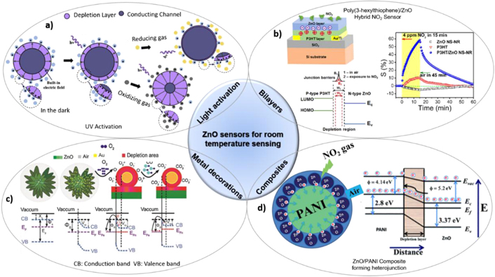
Figure 4. Schematic illustrations of the ZnO sensors operating at room at temperature (a) sensing mechanism of the light-activated sensors (reprinted from [23] Copyright (2017), with permission from Elsevier), (b) device schematic and response of hybrid P3HT/ZnO bilayer sensor (reprinted from [21], Copyright (2016), with permission from Elsevier), (c) Au–metal decoration on ZnO NRs and its sensing mechanism (reprinted from [24], Copyright (2017), with permission from Elsevier) (d) PANI/ZnO composite forming multiple p–n heterojunctions for enhanced sensing performance (reproduced from [20] with permission of The Royal Society of Chemistry).
Download figure:
Standard image High-resolution imageFurther studies indicate that the sensing performance is limited not only by the surface morphology but also the intrinsic electronic and optical properties of ZnO materials. To augment the intrinsic properties of the material, the creation of intrinsic defects was carried out in recent years [18]. As a result, several electronic properties, such as charge transport and surface properties were improved. Such a material engineering technique paves the way to overcome the long-time challenges, mass production of sensors, and controlled synthesis of Ov dominant ZnO structures. High-temperature fabrication is another process challenge; numerous techniques were proposed to grow diverse ZnO NSs at low temperatures. For example, ZnO NRs with high aspect ratio and vertically aligned features [18], were fabricated using a simple vapour transfer approach, exhibited excellent sensing performance towards H2S at RT. In addition, ecofriendly and biocompatible ZnO chemical sensors have also been explored [25].
Selectivity is still an issue with bare ZnO NSs. For instance, bare ZnO NRs sensors were sensitive to both hydrogen and benzene. Through another bilayer approach of targeted molecular sieving, the selectivity was achieved. Khudiar et al employed ZIF-8 to restrict the interferon targeted molecules which have larger kinetic diameters to diffuse through the smaller pores of MOFs. In this report, they demonstrated the selective H2 sensing at RT by allowing its diffusion only through the MOFs over ZnO NRs. The optical sensors based on surface plasmon resonance (SPR) technique can offer high selectivity, as observed in the case of CO detection using ZnO NRs [26]. The major challenge in these optical sensors is the portability for commercial applications.
2.4. Concluding remarks
We have briefly discussed the potential of ZnO materials for gas sensing applications. Although ZnO is considered as the best candidate for gas sensors, the operating temperature that leads to high power consumption and the high cost was a hurdle of bare ZnO sensors. Tremendous efforts include synthesizing NSs, light activation, the use of additive/dopants, the hybridization with other inorganic materials, polymers, and MOFs can be witnessed to reduce the operating temperature without compromising the sensing performance. However, another major challenge to overcome in ZnO gas sensors is the interference of humidity at RM. The development trend of sensors is approaching towards wearable/flexible electronics, which needs the material synthesis procedures to be compatible. For commercialization purposes, advanced methods to enhance sensitivity and selectivity have to be feasible for mass production.
3. WO3 for gas sensors
Chengjun Dong and Yude Wang
Yunnan University, People's Republic of China
3.1. Status
WO3 is an n-type gas sensing material with a wide bandgap. Due to its outstanding semiconductor properties, WO3 has been widely employed for gas sensors in many fields including environment protection, healthcare, disease diagnosis, and food safety [27]. The basic working principles of gas sensors decisively determine their construction and applications. Based on WO3, resistive gas sensors are more popular compared with other types [e.g., microelectro mechanical systems (MEMS) sensor, optical sensors, surface acoustic sensors, and electrochemical sensors] [28], in which the concentrations of target. gas are reflected by the changes in conductivity. The chemical reaction of target. molecules is strongly influenced by the microstructures and surface states of sensing materials.
The morphology and microstructure of WO3 will determine the specific surface area, the amounts of active sites, and the gas diffusion channel, thus affects the sensing outcomes. Therefore, a wide range of synthesis methods have been carried out to prepare different WO3 in 0D, 1D, 2D, 3D and irregular shapes [29], as shown in figure 5. Especially, hierarchical structures with hollow or porous subunits are believed to exhibit superior sensing properties [30, 31]. To achieve morphologies control, templates (e.g., soft templates, hard templates, bio-templates) or additives are efficient strategies to tune the nucleation and growth of unique WO3.

Figure 5. WO3 with different morphologies and common strategies to enhance sensing properties of WO3 gas sensors.
Download figure:
Standard image High-resolution imageThe approaches to enhance the reaction of target. molecules or regulate the charge transfer can effectively enhance the sensing properties (figure 5) [27]. It is well reported that the exposed facet and elemental doping have an ability to regular the surface chemical states of WO3. The noble metal focalization will significantly favour the reaction of target. molecules by spillover effect and electronic sensitization (ES) due to their merits of catalytic characteristics. Essentially, the creation of heterojunctions is a good way to couple WO3 with other sensing materials to tune the electronic structures and interface configuration. 1D WO3 (i.e., NWs, NTs, NRs, etc) is a favourable backbone to support second phases to form a large number of heterojunctions at the interface [32]. Photon activated assisted by light is also a useful option to significantly reduce the operating temperature. Generally, synergistic effects including more than one reasons are fundamental for the outstanding performances.
3.2. Current and future challenges
Efforts to control WO3 morphologies to bring about superior sensing performance is the subject of a large number of concerns. The synthesis processes of WO3 are heavily restricted by the solubility of the available tungsten related precursors. For instance, because of the hydrolysis characteristics, only organic solvents are available to be selected for tungsten chloride. Sodium tungstate dehydrate is another common precursor, however, the solvent is confined to water. Attempts are ongoing to make full use of these precursors and try others as well.
Although diverse morphologies of WO3 in different dimensions for gas sensors have been found in the literature, the main current challenge is that these products are limited to laboratory preparation under severe experimental conditions. If massive production, the aggregation and uncontrollable growth is inevitable. On the other hand, thermal treatment is always mandatory to converse precursors into crystalline WO3. Thus, synthesizing WO3 by one-pot methods is very appealing to simplify the experimental process and reduce the cost.
Parallel challenges we faced must be the improvement in gas sensing performances to meet the requirements for practical applications [33]. The detection capability of low concentrations, high operating temperature, unsatisfactory selectivity and stability are the major bottlenecks. The most cited sensing mechanism is the resistance changes rooted in the reaction between target. molecules and the absorbed active oxygen species. Nevertheless, a big breakthrough is highly expected to provide more fundamental understanding. Admittedly, the sensing properties have been greatly enhanced through several strategies above. Currently, it is still a huge challenge to precisely control the modification, thus the enhancement in sensing properties could be adjustable. Additionally, more studies are needed to survey the specific reasons. Furthermore, integration WO3 with related base to fabricate wearable/flexible sensors to collect comprehensive information simultaneously is a high passionate research topic for personalized health monitoring or medicine in particular.
3.3. Advances in science and technology to meet challenges
Massive synthesis of WO3 with uniformly controllable morphologies to promote its commercial application in gas sensor seems to be unrealistic in short time. Regarding to the precursors, metal tungsten is an alternative source to prepare WO3. WO3 films were deposited from tungsten target as gas sensors by physical and chemical methods, but the microstructures of these prepared films were monotonous. As a soluble substance in polar solvents, amorphous peroxo-tungstic acid obtained by dissolving metal tungstate into hydrogen peroxide is a very promising way [34]. Thermal decomposition of tungsten salt in organic solvents at higher temperature or hydrothermal condition was utilized for one-pot WO3 synthesis [35]. External auxiliary such as microwave-assisted will be helpful to boost the synthesis. These as-prepared WO3 is beneficial to directly coat on textile or polymeric substrates to serve as flexible gas sensors. Moreover, time dependent experiments and controllable parameters should be conducted to reveal the growth mechanism of a certain microstructures and morphologies.
With respect to the gas sensors based on WO3, lower the detection of limitation and operating temperature as well as strengthen the selectivity and long-term stability is still the research topics to be devoted to. Centre on the working principle, any ways to increase the specific surface area and rich the porous structures, especially microporous structure, is worth to have a try to favour the gas molecule diffusion and reaction on the WO3 surface. More suitable additives will be added into to control the crystal plane and amounts of exposed high energy facets. Appropriate doping elements or their co-doping may be attempted to enhance the sensing properties. To fully use the catalytic activities of noble metal NPs, their distribution in WO3 matrix should be regulated. One-pot synthesis of WO3 NPs are easily to fabricate wearable/flexible sensors with/without the help of polymers. Combined with experimental findings, it would enable the gas adsorption/desorption process be investigated using developed computational models such as density functional theory (DFT) [36]. Based on the enhanced sensing strategies, the roles of exposed facets, doping, vacancies, noble metal fictionalization are theoretically simulated, thus the mechanism may be deeply excavated using interdisciplinary knowledge.
On the other hand, using WO3 as active material, MEMS sensor, optical sensor, optoelectronic sensor for various gas detection are less studied so far. These sensors are especially advantageous in selectivity and high-precision detection operated at room temperature.
3.4. Concluding remarks
Here, we have briefly discussed the microstructures and sensing properties of WO3. Although the progresses have been made in controlling the morphologies of WO3, it is still a challenge to expand these synthesis methods for massive production. A series of time-dependent and controllable process conditions will help to explore the growth mechanism in depth. Using metal tungsten as an option of starting material, novel WO3 could be prepared via physical or chemical methods. Hierarchical WO3 with hollow or porous structures are beneficial for the effective gas detection. One-pot synthesis of WO3 is believed to promote the wearable/flexible devices based on WO3. Several common strategies are summarized to enhance the sensing performances of WO3 based gas sensors. Neither the sensing mechanism or the enhanced reasons still need to be deeply understood through computational simulations. Compared to resistive type sensors, the inadequate development in other types of gas sensors based on WO3 requires more attention. As the continuous progresses, we believe that WO3 with desirable sensing properties for practical applications will be controllably synthesized in the upcoming years. Accordingly, future efforts will hopefully include full understanding the growth and sensing mechanism in great details.
Acknowledgments
This work was financially supported by National Natural Science Foundation of China with Grant No. 61761047 and 41876055).
4. Fe2O3-based gas sensors
Qin Kuang
Xiamen University, People's Republic of China
4.1. Status
Fe2O3-based nanomaterials are widely used in gas sensors owing to their high sensitivity, good corrosion resistance, environmental friendliness, and low cost [37, 38]. To date, the existence of four crystalline polymorphs (α-Fe2O3, β-Fe2O3, γ-Fe2O3, and ε-Fe2O3) as well as amorphous Fe2O3 has been well recognized. Among these, α-Fe2O3 and γ-Fe2O3 exist in nature and have attracted much attention, while there have been few studies on the others as gas sensing materials. α-Fe2O3 is the most stable phase and has a rhombohedral corundum structure (space group: R
 ch167), in which Fe3+ ions occupy two-thirds of the octahedral sites confined by the hexagonal close-packed O lattice. Metastable γ-Fe2O3 possesses a cubic, inverse spinel structure with Fd
 m space group. The vacant cation sites, usually located at octahedral sites, are a feature of γ-Fe2O3. Most of them are exposed on the surface, acting as strong adsorption sites [39, 40].
The gas-sensing mechanisms of α-Fe2O3 and γ-Fe2O3 are different due to their different crystal structures. α-Fe2O3 is the surface-resistance-control-type material, and the surface-depletion model is often used to explain its gas sensing mechanism. In contrast, γ-Fe2O3 is the bulk-resistance-control-type material, whose resistance change mainly arises from the conversion between γ-Fe2O3 and Fe3O4 [41]. Fe2O3-based gas sensors generally operate at relatively high temperatures. The phase transition temperature from γ-Fe2O3 to α-Fe2O3 is between 523 and 873 K [38]. This thermal stability problem greatly limits the application of γ-Fe2O3, although its operating temperature can be reduced below the phase transition temperature [42]. Therefore, α-Fe2O3 is potentially the most useful phase of iron(III) oxide for gas sensing applications, and the following discussions are focussed on α-Fe2O3-based materials.
In addition to phase, the morphology of sensing materials, including shape, size, and orientation, plays a crucial role in gas sensing performance. Excellent sensing materials usually possess a large specific surface area and an appropriate porous structure. The former contributes to providing abundant active sites, enhancing gas adsorption, and improving sensitivity, while the latter is favorable for reducing the response/recovery time because of rapid gas molecule diffusion. In the past few decades, great efforts have been devoted to synthesizing various types of nanostructured α-Fe2O3, such as NPs, NRs, NTs, and NFs [38]. The gas-sensing performance of these nanostructured α-Fe2O3 is improved to varying degrees in comparison to bulk α-Fe2O3. Recently, it has been recognized that a large specific surface area cannot ensure an improved gas sensing performance of α-Fe2O3. Other factors related to the surface are also important, such as surface energy, surface atomic arrangement, and dangling bond density. However, it is difficult to explore the specific roles of these factors in randomly oriented nanomaterials. Hence, shape-controlled α-Fe2O3 nanocrystals (NCs) with specific exposed facets have gradually attracted the interest of scientists.
4.2. Current and future challenges
α-Fe2O3-based gas sensors have been widely used in detecting various gases, such as H2, NO2, H2S, and volatile organic compounds (VOCs). However, there are still some obstacles to overcome in future research. Nanostructures usually contribute to enhanced gas-sensing performance. However, most nanostructures easily stack together spontaneously to reduce their overall surface energy. Such densely stacked structures decrease the specific surface area, obscure active sites, and influence gas diffusion, thereby weakening the intrinsic gas sensing performance [42]. There is therefore current interest in the rational design of large specific surface area NSs that can make full use of their sensing ability for developing high-performance α-Fe2O3-based gas sensors.
Exposing the surface of high-energy facets has proven to be an effective approach to improve the performance of gas sensing materials. As for α-Fe2O3, NCs with exposure to well-controlled surfaces, such as {012}, {104}, {113}, and {001}, have been investigated to date [43]. The facet-dependent gas sensing of α-Fe2O3 NCs strongly depends on the variation in atomic configurations and chemical composition of different facets. However, owing to the complicated crystal growth environments and uncertain roles of various influencing factors, the synthesis of α-Fe2O3 NCs with specific exposed facets mainly depends on trial and error at present [44]. It is still a great challenge to synthesize α-Fe2O3 NCs with a high percentage of exposed active facets without capping agents. On the other hand, the surface terminations, including atomic structures and chemical compositions, are quite complex in real environments when solvation reactions and/or surface reconstruction are considered. Thus, analyzing the surfaces of ideal crystals is unlikely to be sufficient to explain the facet-dependent sensing properties of α-Fe2O3 NCs.
Pure α-Fe2O3-based gas sensors are usually very cheap and exhibit good sensitivity, but most of them have higher operating temperatures and have limited selectivity and long-term stability [38]. The optimal operating temperatures of reported α-Fe2O3-based gas sensors are approximately 200 °C and higher, due to the need to balance the effect of activation energy and gas molecule adsorption. In consideration of energy costs, environmental protection, and safety, an excessively high operating temperature is not practical. Selectivity is an important consideration in α-Fe2O3-based gas sensors. It is often difficult to quantify the complex characteristics that determine selectivity. Many factors influence selectivity, such as the reaction process, adsorption capacity, bond dissociation energy, pore size, and consumed number of chemisorbed oxygen species [42]. Low stability and long-term signal drift will result in uncertain results and false alarms, and the need for the sensors to be recalibrated frequently. Thus, Fe2O3 gas sensors should have excellent long-term stability for up to 2–3 years to meet the demands of practical applications, including stability in high operating temperatures, humid environments, and corrosive media [38]. However, little attention is paid to stability in reported studies, with stability of α-Fe2O3 reported in literature only over a matter of weeks.
To address the challenges mentioned above, new strategies need to be developed. Assembling NRs, NWs, and NSHs into 3D hierarchical nanostructures of α-Fe2O3 with a large active surface and appropriate porous structures is an effective approach to solve the problem of easy stacking of nanomaterials. Many studies have proven the superiority of such structures [42]. Apart from exposing more active surfaces, the well-aligned porous structures among adjacent units serve as unimpeded passages, which facilitates rapid gas diffusion.
A recent study found that the surface energy of as-prepared micro- and nanocrystals is correlated with the supersaturation of growth units, and high supersaturation is conducive to forming high-energy surfaces [44]. As shown in figure 6(a), with the increase in supersaturation, the as-formed α-Fe2O3 NCs are gradually transformed from nanoplates with stable {001} facets to pseudocubes and hexagonal bipyramids with higher energy {012} and {113} facets, respectively [45]. For highly energetic facets, the loss of original singly coordinated O atoms produces coordinatively unsaturated Fe atoms with dangling bonds. The higher density of low-coordinated Fe atoms gives rise to an excellent ability to adsorb oxygen and other gas molecules, resulting in enhanced performance (figures 6(b)–(d)) [45]. The sensitivity and selectivity of α-Fe2O3-based gas sensors can be further improved with a deeper understanding of surface-enhanced gas sensing when combined with other modification strategies.
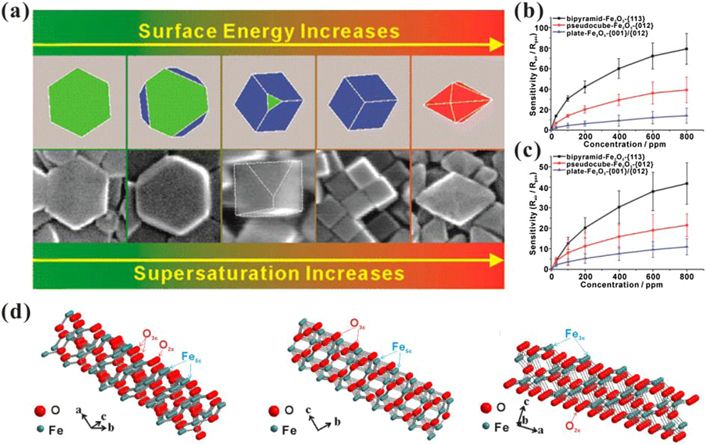
Figure 6. (a) Schematic of the supersaturation-controlled morphology evolution of α-Fe2O3 NCs from {001} to {012} and {113} facets. (b) and (c) Concentration-dependent sensing curves of different shaped α-Fe2O3 NCs towards acetone and methanol, respectively. (d) Surface terminations of {113}, {012}, and {001} of α-Fe2O3. Reprinted with permission from [45]. Copyright (2014) American Chemical Society.
Download figure:
Standard image High-resolution imageApart from morphology control, constructing heterojunctions is also a common method to overcome the inherent problems of pure α-Fe2O3 gas sensors. There are many studies in which metal/α-Fe2O3 and metal oxide/α-Fe2O3 gas sensors are conducive to reducing operating temperatures, shortening the response/recovery time, and improving selectivity [46]. In contrast, reports on polymer/α-Fe2O3 gas sensors are still rare. Low conductivity and poor stability of organic materials, high operating temperatures, and complicated processability of inorganic materials limit their development. Surprisingly, a hybrid of these two classes of materials can negate their individual disadvantages to some extent and lead to enhanced performance, especially resulting in greatly reduced operating temperatures. Thus, polymer/α-Fe2O3 is a promising material for gas sensors working at RM [38].
4.3. Concluding remarks
α-Fe2O3 is the most promising phase of ferric oxide in gas monitoring areas. Nanostructured α-Fe2O3 generally has greatly improved sensitivity and dynamic response. Therefore, proper design of nanostructures, especially hierarchical NSs with a large proportion of exposed high-energy facets, is an effective approach to enhance the performance of α-Fe2O3-based gas sensors. In addition, introducing other components (noble metals, MOS, or conducting polymers) can partly avoid or improve the inherent shortcomings of pure α-Fe2O3, such as high operating temperatures and low selectivity. Although α-Fe2O3-based gas sensors are already widely used, it is still important to develop higher performance sensors to meet future needs and improve the accuracy of measurements.
Acknowledgments
This work was supported by the National Key Research and Development Programme of China (2017YFA0206801), and the National Natural Science Foundation of China (No. 21671163).
5. Chemiresistive CeO2-based gas sensors
Zamaswazi P Tshabalala3, David E Motaung1,3
1University of the Free State, South Africa
3University of Limpopo, South Africa
5.1. Status
The necessity for detection and continuous monitoring of lethal and combustible gaseous substances has become more vital over the years for the drive of public and domestic welfare, industrial developments, and environmental monitoring for air pollution. Currently, chemiresistive gas sensors based on MOs are more appealing. Among the MOs, cerium oxide (CeO2) which is a rare-earth oxide compound vastly abundant on the Earth crust has gained attention in gas sensing field. CeO2 is a widely used catalyst with impressive physical and chemical properties such as, the unique electronic configuration in the 4f shells, ample amount of oxygen vacancies (Ov) and dual valence state Ce4+ and Ce3+ giving rise to its extraordinary redox properties [47–49]. Catalytic ability of CeO2 highly influences the chemisorption of the oxygen molecules and reactant gas during the sensing process. Currently, numerous works has been done using CeO2 based sensors, for detection of toxic and flammable gases, such as CO, H2S, formaldehyde, operating at temperature higher than 100 °C [47–50]. Few studies have been done on pristine CeO2 focussing on low operating sensing temperature (⩽100 °C) [51]. CeO2 NPs synthesized using chemical precipitation method showed high sensor response at RT towards H2S, CO, NO2 and isopropanol (IPA) gas (figure 7(d)) [51]. Hybrid materials formed by CeO2-heterostructures showed RT operation towards NH3, NO2 and CO, using CeO2 NPs coated by cross-linked polyaniline (PANI) hydrogel, CeO2/graphene heterostructure and Pt NCs on CeO2 nanowire, respectively [52, 53]. Gas sensing mechanism is surface dependent, thus, maximized sensitivity requires improved surface area and porosity, and surface functionalization. Pristine CeO2 nanospheres with surface area of 773.3 cm3 g−1 displayed enhanced sensitivity towards 30 ppm CO [47]. Motaung et al [49] reported on ultra-high sensitivity and selectivity to H2 induced by CeO2–SnO2 heterojunction. The {100} facet in CeO2 exhibited high surface energy, influencing the decomposition of analyte gas. Zhang et al achieved RM NO2 sensing driven by CeO2–graphene with exposed {100} polar facets. Besides, the CeO2–graphene nanocubes exhibited plentiful amount of Ov, which expedited the adsorption of NO2 on the surface, such that sensitivity increased with Ce3+ concentration [53]. Elger et al showed the potential of joint operando Raman-gas-phase FTIR spectroscopy to clarify the mode of operation of 0.5 wt% Au doped CeO2 during ethanol gas sensing, where the presence of Ov in CeO2 were directly monitored, in addition the surface species [54]. In terms of selectivity, by using heterostructures and surface loaded CeO2, improved selectivity was witnessed. Jayababu et al [55] reported on NiO decorated CeO2 nanostructures with superior sensitivity to 1–100 ppm IPA. Figure 7(a) shows improved selectivity towards IPA among other VOC's, by 11 folds increase in response from 139 to 1570 for NiO–CeO2 nanocomposite. With regards to response and recovery times, CeO2–SnO2 heterostructure showed fast response and recovery times to H2 at 300 °C [49]. Similar results were displayed by CeO2 decorated by NiO NPs exposed to IPA at RT (figures 7(b) and (c)) [55].

Figure 7. (a) IPA selectivity plot due to NiO-decoration on CeO2. Response and recovery times of (b) pure CeO2 and (c) NiO–CeO2. (d) 15 monthss stability test of pristine CeO2 towards 30 ppm CO at 400 °C. (e) Schematic diagram of various nanomaterials-based sensor array for medical diagnosis by analyzing human breath. (Reproduced from [55] with permission of The Royal Society of Chemistry, reprinted with permission from [47]. Copyright (2018) American Chemical Society.)
Download figure:
Standard image High-resolution image5.2. Current and future challenges
Despite the several positive properties that CeO2 possess, nonetheless, it is more prone to achieve optimum response at high operating temperatures of 200–700 °C, making it unattractive. Since it compromises the material's stability, adhesion to substrate, lifetime of the sensor, leads to high power consumption and may ignite in the presence of combustible gases. The current achievable response and recovery times on CeO2-based sensors need to be improved further as to reach ultra-fast (<1 s) response kinetics. This is justified by the toxicity of analyte gas and field of application (indoor air quality, process monitoring, medical diagnosis, food safety), there are time based limits, such as 10 ms threshold response time for O2 monitoring in order to control combustion in cylinders of two-wheeled vehicles engines [56]. A sensor needs to maintain its response and resist change whether in phase due to heat or segregation of dopants and chemical change due to poisoning during reactions, therefore long-term stability is of great importance for commercial applications as it guarantees a prolonged the sensor lifetime. While the CeO2 nanospheres presented by Majumder and Roy [47] displayed (figures 7(c) and (d)) great stability in baseline resistance and sensitivity with standard deviation less than 2 over 15 months under 30 ppm CO at 400 °C, however, the high operating temperature still indicate a limitation.
Furthermore, the cross-sensitivity to relative humidity (RH) also remains a significant challenge, more especially at low operating temperatures <100 °C. Since water from RH get physiosorbed and occupy the active sites of the sensing material, thus decreasing the sensor response. Additionally, the gas selectivity is a universal challenge even to other MOS based sensors, and this limit their commercialization, as a result, significant amount of work is required in order to accelerate the commercialization. Additionally, to accomplish accurate and reliable gases sensor outputs CeO2 based nanoarrays should be considered. Nanoarrays enable smart sensing by integrating multiple sensors each selective to a specific targeted gas and a GCMS to quantify the concentration of each parameter, such as analyte gas and RH (figure 7(e)). To properly achieve nanoarrays, further miniaturization is required for portable, light weight devices and this owes to achieving smaller particle sized morphologies (QD), large surface area exposed for analyte gas and stable sensor performance [57].
5.3. Concluding remarks
Owing to its chemical and physical properties, such as catalytic activity, dual valence state Ce4+ and Ce3+ and high concentration of Ov, CeO2 demonstrated potential and sustainability in gas sensing application. Further research still needs to be conducted to address the aforementioned challenges, such as improving operating temperature and selectivity, rapid response time and long-term stability and RH. RT gas sensing is attractive from the standpoint of low energy consumption, streamlined sensor fabrication without the requirement of a heating component, and thus low cost can be anticipated. Moreover, synthesis of nanostructures in a controlled way, particularly for commercial devices is tremendously important. The concept of exploiting metal additives, (e.g. Ni) to improve the moisture-resistant of the MO gas sensors is overbearing and is ought to be considered cautiously as well. This may advance to close the gap between the research and practical application.
Acknowledgments
The National Research Foundation is also acknowledged for financial support.
6. Tin dioxide-based gas sensors
Xianghong Liu1 and Junliang Yang2
1Qingdao University, People's Republic of China
2Central South University, People's Republic of China
6.1. Status
Among the many metal oxide semiconductors (MOS), SnO2 is the most broadly used material in chemiresistive gas sensors ever since the first development of the commercial sensor devices, i.e. TGS 109 utilizing a sintered SnO2 pellet with embedded electrodes and heaters as the sensing elements, by Naoyoshi Taguchi in the 1960s due to its high sensitivity, cost effectiveness, and good thermal stability compared with other MOS [58, 59]. Starting from the beginning of 20th century, the research in gas sensors expanded significantly with a fast-growing number of yearly publications. A survey from Web of Science reveals that publications of 'SnO2 gas sensors' during 2000–2020 accumulates to a total number of over 6500, followed by a number of 6100 from ZnO which is also extensively investigated for gas sensors.
Nanostructured materials can afford many advantages when applied as the sensing layers in compared to the conventional thick-films, due to the large surface area, high surface reactivity, tunable porosity and dimensionality. As a result, enormous effort has been explored to synthesize SnO2 nanomaterials, NPs, NWs, nanosheets, and other nanoarchitectures. The gas sensors based on these SnO2 nanostructures have displayed improved '4s' parameters [60], i.e., sensitivity, selectivity, response–recovery speed and stability, for detection of various gaseous molecules such as H2, NO2, CO, CH4 and VOCs. For instance, the nanorods or NWs are more resistant to thermal ripening and aggregation than NPs at the operating temperatures, usually higher than 300 °C, which would deteriorate the sensor performances due to the loss of surface area of sensing layers. The porous nanostructures have abundant internal channels to facilitate the mass transfer and gas diffusion [4], as well as increased accesses to external molecules, thereby leading to faster response speed and higher sensitivity.
In order to improve the sensor performances, noble metals such as Au, Pt, and Pd have been widely employed as a sensitizer for SnO2 materials either by electronic or chemical sensitization (CS) mechanism [61]. The fabrication of heterostructures from SnO2 and other MOS were also beneficial for better sensors due to a synergic effect [62], which has been demonstrated by numerous studies. Apart from the well-known grain size effect [61], the manipulation of the thickness of sensing layers comparable to the Debye length also results in a higher sensitivity.
6.2. Current and future challenges
Despite of the extensive research for over 50 years, the sensing mechanism of metal oxide sensors is still to be clarified. Although the trial-error approach can be useful in developing more sensitive materials, a thorough understanding of the fundamentals of sensors can lead to knowledge-based approaches. The widely accepted mechanism for SnO2 sensors is ascribed to the reaction of molecules with surface oxygen species (O2 −, O− and O2−), which alters the carrier density and the size of electron depleted layer or hole accumulation layer (HAL), hence modulating the conductivity of the sensing layers [63]. Since the ionized oxygen species are responsible for the sensing reactions, a clear knowledge of their generation and reaction pathway is very important. When noble metal catalysts are incorporated in sensing materials, their functions and how they contribute to the sensor reactions are still not clearly understood and more efforts are needed to clarify their roles.
Although SnO2 gas sensors have some merits such as high sensitivity and good thermal stability, as well as miniaturized size compared with analytic instruments such as gas/mass chromatography, they suffer from the lack of selectivity due to its sensing mechanism. Selectivity turns out to be very important when gas sensors are applied to exhaled breath diagnosis to screen potential diseases or disorders in human bodies [64]. An accurate detection of the VOCs biomarkers is thus of great significance, considering the exhaled breath normally consists of many interfering molecules such as CO2, O2, and H2O, as well as other molecules from metabolism.
In order to activate the SnO2 sensors, a high temperature normally in the range of 300–500 °C is required. This indicates a high-power consumption considering the conventional gas sensors generally need a typical power of hundreds of mW. The demands for integration of gas sensors into smart electronics such as mobile phones requires a power low enough to be powered up by a battery or even by nanogenerators integrated in wearable devices [65].
6.3. Advances in science and technology to meet challenges
Noble metal catalysts are always needed in a real sensor (e.g. Pd has been essential in the SnO2 gas sensors from Figaro) to enhance the sensor performance, this has propelled enormous research effort to investigate other catalysts such as Au and Pt. Sensing mechanisms can be different and complex considering the diverse electronic structure, size and morphology of the catalyst, as well as the electronic or catalytic interaction with the host materials. This is why today many controversial results can be found in the literature. To better understand the structure–property correlations, experiments or test systems with in situ and operando techniques might be useful to rationalize the details behind sensing reactions.
Selectivity of MOS sensors can be improved by using a molecular sieve layer such as zeolites or MOFs and this has been demonstrated by many publications. Alternatively, by incorporating a gas sensor array with integrated circuits and data analysis system, the electronic nose (e-nose) can become very selective [66]. The independent and different response features of individual sensors are subject to logic analysis through a pattern recognition method. Based on the MEMS technology, the e-nose can be fabricated from various modified SnO2 sensors with different sensing characteristics. This will largely improve the detection accuracy in a very complicated situation such as the exhaled breath diagnosis [67].
Gas sensors are currently being developed to have more functions such as flexibility, deformation and compatibility for integration into smart electronics like mobile phones and watches. The MEMS technology makes it possible to produce sensor devices with very small size and easy integration into portable electronics or sensor networks (internet of things). Furthermore, the MEMS sensors generally have a much low power consumption. For example, the TGS 8100 sensor has a power consumption of 15 mW, which is significantly lower than the 210 mW of TGS 2600. With the advance of MEMS design or working under a pulse-heating mode, a power consumption of several mW or even lower is also possible.
Currently RT gas sensor has aroused much interest since it does not consume any power for heating. It also helps simplify the fabrication and lower the cost of sensors because heater is not needed at RT operation. There are already some reports showing the potential of SnO2 materials for RT gas sensors under the optical illumination or by incorporating carbon NTs or graphene, or by Ov engineering.
6.4. Concluding remarks and prospects
SnO2 has been the most popular materials in practical gas sensors, and probably it will continue to play a dominant role in future sensors due to its tunable structure and peculiar sensing properties. More efforts are needed to obtain a clear knowledge of the sensing mechanism with more powerful analysis techniques, as well as theoretical simulation. MEMS gas sensors based on SnO2 with low fabrication cost and low power consumption will be of great importance for artificial e-noses, portable electronic devices, and wireless sensor network. Considering the limited area of the sensing layers in an MEMS device and the important effects of materials microstructure on the receptor and transducer functions, new technology to deposit nanostructured SnO2 sensing layers rather than the conventional thick-films that is compatible with MEMS process or flexible substrates will be essential. With time, the application of SnO2 sensors to practical non-invasive diagnosis as well as other areas, which requires exclusive detection accuracy and selectivity, may can be realized through pattern recognition, machine learning, and optimized algorithm method, etc.
Acknowledgments
This work is supported by the National Natural Science Foundation of China (Nos. 51972182 and 61971252).
7. TiO2 for gas sensors
Haitao Fu1, Xiaohong Yang1,2, Xizhong An2
1Key Laboratory for Ecological Metallurgy of Multumetallic Mineral, Ministry of Education, Northeastern University, People's Republic of China
2School of Metallurgy, Northeastern University, People's Republic of China
7.1. Status
TiO2 is a typical n-type semiconductor and mainly exists in three crystal forms (e.g., rutile, anatase, and brookite phase). Among them, anatase and rutile TiO2 (bandgap of 3.2 and 3.02 eV) are regarded as promising functional materials (especially for nanomaterials) due to their excellent instinct properties (e.g., high stability, harsh environmental tolerance, and environment-friendly), which impart them diverse cutting-edge applications [68]. In the past decades, sensors are one of the most popular applications for TiO2, and have been widely investigated. Based on sensing principles, TiO2 is capable to be utilized as various types of sensors (biological sensors based on electrochemistry, gas sensors based on chemi-resistors, and COD sensors based on optical properties). For gas sensors, the vast majority of TiO2-based gas sensors are developed as resistance type metal oxide gas sensors (also called chemi-resistors), which achieve detection by the change of the resistance of sensing materials when exposed to the targeted gases. Such a gas sensor normally works in the temperature of 150–400 °C.
Similar to other semiconductor gas sensing materials, the sensing mechanism of TiO2 is described as a two-step process (receptor and transducer process, as illustrated in figure 8), which corresponds to surface reaction (adsorption and reaction) and electron transfer, respectively [69]. The electrons of TiO2 are excited by heat from the valence band (VB) to the conductive band (CB). Oxygen molecules in the air react with the electrons on the surface to form chemisorbed oxygen ion species (O−, O2 −, or O2−), which are related to the working temperature. In this chemical adsorption process, electrons of TiO2 are trapped on the surface, leading to high resistance compared to that in vacuum or inert gas atmospheres. At this stage, if reducing gases (H2, H2S, NH3, CO, and VOCs) are introduced, the resistance of TiO2 will decrease since the trapped electrons are released back to CB by the reaction between oxygen ion species and the reducing gases; on the contrary, the resistance will further increase if exposed to oxidizing gases (NO2, O2, and O3) because more electrons are captured on the surface. The amount of resistance change reflects the sensitivity/response of a sensor.

Figure 8. Schematic images of gas sensing at different modes, where L represents the depletion layer, R represents particle size, and DN corresponds to the diameter of the neck cross section. Reproduced from [69]. CC BY 4.0.
Download figure:
Standard image High-resolution imageThe transducer process, related to the electron transfer in the sensing materials, can be illustrated by three modes: surface-controlled mode, grain-controlled mode, and neck-controlled mode. Which mode plays the dominant role is dependent upon the particle size. Nowadays, the active sensing layers of TiO2-based sensors are basically manufactured by NPs, among which the neck resistance (neck-controlled mode) plays a key role in the contribution of whole resistance.
Based on the sensing mechanism, two-aspect efforts have been made for enhancing the sensing performance, i.e., (1) controlling the morphology of TiO2 NPs to pursue large surface area or expose large area of the certain lattice plane which strongly interacts with targeted gas molecules [70, 71]; (2) transferring more electrons to the surface of TiO2 NPs.
For morphology control, various novel TiO2 nanostructures, including 0D, 1D, 2D nanostructures, and 3D hierarchical microstructures, are prepared as gas sensing materials via various physical and chemical methods. A good example can be demonstrated via a butterfly wing structure of TiO2, which has been constructed by a biological template for fast detection of acetone at RM [72]. Furthermore, for practical use (in MEMS or wearable sensors), TiO2-based sensing materials are always packed or prepared in thin films [73].
To let electrons transfer to the surface, a variety of methods are introduced, including the formation of heterostructures, element lattice doping, and UV irradiation assistance [74]. Fabricating heterostructures are the most commonly used strategy to enhance sensing performance. Two types of TiO2-based heterojunction are widely reported, i.e., nanoparticle surface modification and core–shell structures [75]. The guest materials involve noble metal NPs (Au, Pt, Ag, Pd), transmit MOS (SnO2, ZnO, V2O5, Fe2O3 etc), carbon materials (CNTs, graphene oxides, and carbon QDs), and semi-conductive polymers. The main contribution of the heterostructures sensing mechanism can be attributed to electron sensation and chemical sensation. Generally, when the heterojunction forms, the Femi-level of two materials reaches equilibrium, leading to band bending. Electron transfer occurs from the materials with high work function to the other one, increasing depletion layers and improving sensing performances. The heterojunction can also improve gas diffusion in the structure, introduce more Ov of TiO2, and increase active surface area (spillover effect).
UV irradiation assistance is another way to increase charge transfer. The idea is inspired by the excellent photocatalytic properties of TiO2. UV irradiation can effectively excite electrons from the VB of TiO2 to CB at low temperature, further achieving transformation electrons to the TiO2 surface. This is also a physical assistant way to lower the working temperature of TiO2-based gas sensors. As above mentioned, combining these strategies into a product could be an effective way to improve sensing performance.
7.2. Current and future challenges
Of achieved so far, challenges still exist in TiO2-based gas sensors. High sensitivity (especially at low concentration) is the main pursue in the current and future research, particularly in medical diagnosis. The diagnosis by gas sensors is based on the analysis of the VOCs (ppb level) in human's exhaled gas [76].
Why TiO2-based sensing materials are sensitive to various targeted gases in different reports need to be well answered. For example, some articles demonstrate that TiO2 nanostructures or nanocomposites are sensitive to ammonia; while others report that TiO2 based materials show high sensitivity to acetone, even though ammonia exists.
For practical use (especially for wearable gas sensors by combining with 2D materials), the reliability of TiO2 nanocomposites is a key issue. Researchers try to keep the stability of high-performance TiO2 nanocomposites via purposed pre-treatments, such as UV irradiation treatment for firmly bonding TiO2 and guest materials, and high-temperature annealing [77]. But further investigations are still required.
Improving the sensitivity of TiO2-based sensors is the main vision for current research. To the view of materials, as aforementioned, morphology control and heterostructures are the main strategies used. It is noted that heterojunctions may improve not only sensitivity, but also response time, the limit of detection (LOD), and even lower working temperature.
The mechanisms of the selectivity and low-temperature detection of the TiO2 nanocomposites must be better investigated. Opinions are divided as to which gases show better sensitivity/response to certain TiO2-based materials. Besides, many articles demonstrate TiO2 sensing materials can detect targeted gases at low (room) temperature. However, the reasons are always missing. Two kinds of techniques may offer help: in situ techniques (in situ XPS, UV, FTIR) and first principle computational simulation.
7.3. Concluding remark
TiO2-based gas sensors have been intensively explored in the past decades. There are still challenges to be addressed, such as the development of novel nanostructures, detection at low temperature, ultra-high sensitivity, the stability of heterojunction, and the fundamental understanding for high-performance sensing behaviours.
Dependent upon the specific use of sensors, it is not necessary to combine all the excellent performances (high sensitivity, fast response and recovery, low LOD, wide dynamic range, etc) in a sensor. However, the high selectivity is always required for practical applications. Therefore, the fundamental understanding of selectivity is crucial for the TiO2-based gas sensors. In addition, the breakthrough of the fundamental mechanism will play a decisive role in the development of gas sensors' new applications (medical diagnosis) and wearable devices.
Acknowledgments
We acknowledge the support by National Natural Science Foundation of China (Nos. 51974086) and the Fundamental Reserch Funds for the Central Universities (N2125027).
8. CuO for gas sensors
Shiqiang Zhou, Baoye Zi and Qingju Liu
Yunnan University, People's Republic of China
8.1. Status
Various types of hazardous gases, such as NO2, NH3, H2S, H2, CO and VOCs, are routinely and daily released from industrial and agriculture processes, or emitted as vehicle exhaust emissions. Therefore, detection of hazardous gases and pollution of environment in situ and real time have motivated us to develop high-precision gas sensors devices with good selectivity, fast response, high sensitivity, low LOD. The first commercially available gas sensor device was introduced in the 1962s using metal oxide as the sensing layer [78]. The research in the field of gas sensors has grown rapidly in the latest years; CuO is one of the most representative p-type metal oxide semiconductors, which has been extensively studied in various fields especially as an effective and affordable material for gas sensor. Up to now, the p-type MOS CuO used in gas sensing have been mainly monitoring targeted gases, including H2S, CO, NO2, CO2 and NH3 (figure 9(a)). Generally, p-type CuO offers poor selectivity, low response, long response time, high working temperature to targeted gases, and they are not very popular for sensing applications especially in pristine form, which causes great concern on the gas sensing performance of CuO method. As of today, it has been realized that a good pathway for sensing enhancement is developed with p–p homojunction, n–n as well as n–p heterojunctions via loading semiconducting nanomaterials or modification of the semiconductor metal oxide with noble metals. Figure 9(b) shows the number papers concerning CuO-based gas sensors published from 1995 to now.
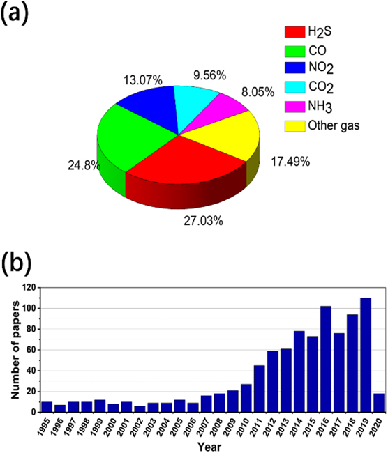
Figure 9. The copper oxides: (a) schematic view of the CuO-based gas sensors for detection of various hazardous gases and (b) the number of papers related to CuO-based gas sensors from 1995–2020 (data from web of knowledge.com) from 1995–2020; here, the papers searched from the web of science refined by 'title = gas sensor and CuO' with all document types on March 15, 2020.
Download figure:
Standard image High-resolution image8.2. Current and future challenges
Currently, a great progress has been made in understanding the mechanisms and designing of CuO gas-sensitive materials. New mechanistic studies that lead to potential solutions to overcome the existing issues of CuO. Oosthuizen et al [79] affirmed that CuO sensor response/sensitivity is dependent on the average crystallite size and specific surface area which resulting in a reduction of the charge carrier concentration, giving rise to a more pronounced change in CuO sensor resistance as validated by Hall effect analysis. Anisotropy is a basic property of single crystals. Dissimilar facets/surfaces have different geometric and electronic structure that results in dissimilar functional properties. Yin and Liu [80] studied that the enhanced ethanol sensing performance characteristics are obviously dependent on the low index (111) facet with high activity relative to high index (202) facet of CuO microstructures. Crystal quality and surface defect density also play important roles in gas sensing performance. Dhakshinamoorthy and Pullithadathil [81] reported a comprehensive H2S gas sensing property analysis of CuO nanocuboids to explore the sensing mechanism and gas/material interaction as a function of temperature. Strong catalytic activity of CuO (111) surface towards the dissociation of O2 and H2S molecules make the monoclinic CuO nanocuboid a highly selective material towards H2S gas sensing. Oosthuizen et al [82] unambiguously demonstrated that the gas sensing activity of CuO is determined by the nature of surfaces exposed to ambient gas. Accordingly, a control over crystal morphology, i.e. over the angular relationships, size and shape of faces in a crystal, is required for the development of better sensors with increased selectivity and sensitivity in the chemical determination of gases. It is mandatory to understand mechanisms and find out its kinetic pathway on different gas. However, the attention of mechanism research on specific gas species is still insufficient.
Several long-standing issues in gas sensor of CuO need to be overcome to develop a practical excellent performance CuO gas sensor, including long-term stability caused by gas poisoning and other factors, and temperature and humidity effects. For further improvement of sensing performance, they have been modified using noble metals, metal ions, and other materials. Composites of multi-phase CuO have also been frequently reported. Adamu et al [83] reported a sensor for NO2 detection based on a p–p heterojunction consisting of tertiary Cu3Mo2O9 micro/nanorods vertically aligned on a continuous CuO layer using a simple, cheap, and catalyst-free chemical vapour deposition (CVD) technique. The performances for NO2 gas are quite outstanding compared to those reported for the metal oxide-based semiconductor sensors. This study would further enrich the sensitive materials as a gas sensor and provide a simple and cheap way to fabricate micro/nanorod array-based gas sensors. Kim et al [84] reported H2S gas sensing characteristics of RGO loaded CuO NFs. Besides large surface area of RGO and plenty of dangling bonds, work function difference between RGO and CuO will results in formation of plenty RGO–CuO heterojunctions, where electrons from CuO will transfer to RGO and accordingly a HAL will develop on CuO. When exposed to H2S, conversion of CuO to CuS changes the conductivity from semiconducting to metallic type and destroys the established heterojunction, leading to a high response to H2S. Choi et al [85] fabricated high-resolution p-type CuO/Cu2O nanopattern channels decorated with Ag NPs using a low-energy argon ion bombardment process via a unique top-down lithographic approach for high-performance sensing of VOCs (figure 10). The high-resolution CuO/Cu2O/Ag nanopattern sensor showed improved sensitivity from minimum 2.9 to maximum 7.7 times for various VOCs compared with the pristine CuO/Cu2O nanopattern. This explains the key role of the noble metal dopant in inducing electronic and CS effects on the entire sensing channel and improving the performance of VOCs gas sensors.
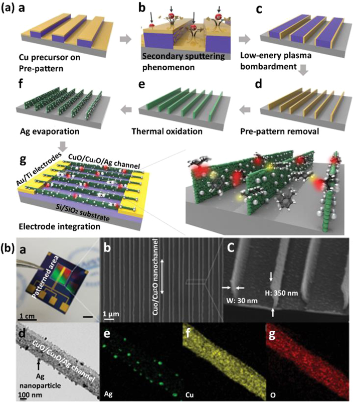
Figure 10. (a) Schematic of the fabrication process for CuO/Cu2O/Ag nanopattern sensors. (b) Photographic image of a representative gas sensor and SEM images of the CuO/Cu2O/Ag nanopattern. [85] John Wiley & Sons. [Copyright © 2019 WILEY‐VCH Verlag GmbH & Co. KGaA, Weinheim].
Download figure:
Standard image High-resolution imageRecently, CuO thin film gas sensors have been studied to detect various gas. The most important feature of the CuO thin film gas sensors is their possibility to function at low or RMs for a long time. Recently published reports have shown that pure CuO, as well as modified/doped CuO films can be developed by various techniques, which also increases the possibility to develop gas sensors. Ponmudi et al [86] reported on the properties of thin Cr2O3:CuO films prepared by radio frequency magnetron sputtering technique, which suggests that the radio frequency magnetron sputtered Cr2O3:CuO thin films can perform efficiently as an ammonia gas sensor at RM. Choi et al [87] fabricated a CO gas sensor using CuO thin film deposition onto a flexible polyimide substrate using a kinetic spraying process. This work would play a pioneering role in disseminating knowledge in the field of CO gas sensors using a kinetic spraying method.
Although great progress has been made in improving CuO sensing performance by trying a mass of related various methods, which include using metal ion doping CuO, noble metal modifying, and composites with other materials, the bottleneck still exists in current gas sensing systems for further improving performance. Many gas sensing mechanisms of CuO based materials with various sizes and morphologies have been presented to explain their sensing properties. However, it is not clearly elucidated why the same CuO based materials with similar sizes and morphologies show markedly different sensing properties. Moreover, interfering gases often affect the sensing performance, resulting in a drastically reduced response, which causes great concern on the selectivity of gas sensors. As a result, it is of key importance for detection of multiple gases to construct reliable gas sensing devices with asymmetric structures and disparate sensing outputs, a goal that is yet to be achieved. In addition, long-term stability and durability studies are far from meeting the requirements of industrialization under varying environmental conditions, such as different temperatures and humidity levels.
8.3. Concluding remarks
From what have been discussed above, we can realize the CuO is a promising gas sensor for detecting various harmful gas. With the tremendous efforts of scientists and the development of in situ instruments characterizations and theory calculations, it is very possible to clearly reveal the complicated mechanism of gas sensing, design and prepare CuO gas sensor with low cost, good sensitivity, fast response/recovery time, long-term stability for fabrication of future gas sensing and other sensor-related devices.
Acknowledgments
This work was supported by National Natural Science Foundation of China (No. 51562038), Yunnan Key Project of Natural Science Foundation of Yunnan (2018FY001(-011)).
9. NiO for gas sensors
Mario Urso
Università di Catania, Italy
9.1. Status
Nickel oxide (NiO) is a wide bandgap (3.6–4.2 eV) p-type metal oxide semiconductor where holes are the majority carriers due to the presence of Ni vacancies in the cubic crystal structure. NiO has high chemical and thermal stability, low dependence on humidity, and unique optical, electrical and magnetic properties [88]. Moreover, NiO nanostructures with large surface area, porous structure and low amount of material can be prepared by calcination of precursor nanostructures grown by low-cost methods, among which chemical/co-precipitation, hydrothermal/solvothermal synthesis, sol–gel, etc. Owing to their exceptional properties, NiO nanostructures have been frequently used as sensing material for chemoresistive gas sensors, which are attracting enormous attention in a wide range of applications, including medical diagnosis, environmental monitoring, industrial processes, etc. Among the different targets of NiO-based gas sensors are VOCs such as ethanol, acetone, toluene and xylene, highly toxic gases such as CO, NO2 and H2S, and combustible gases such as H2 and methane. In particular, NiO nanostructures have shown remarkable performance as acetone sensors operated at high temperature for non-invasive diagnosis of diabetes by human breath analysis [89], and as NO2 sensors operating at RM for indoor and outdoor air quality monitoring [90].
As for all other gas sensors, researchers have developed several strategies to achieve as many as possible of the ideal characteristics of a sensor, i.e. high sensitivity, selectivity and stability, low LOD, short response and recovery time. Above all, the sensitivity has attracted great attentions since p-type semiconductors have a lower sensitivity than n-type [5]. The most effective strategies to obtain high performance with NiO-based gas sensors include:
- (a)Nanostructure morphological design: NPs, NWs, nanorods, nanosheets, porous thin film, etc with large surface area offer a higher number of adsorption sites for the gas molecules and thus higher sensitivity, in principle [88];
- (b)Doping with metals (Al, Cr, Fe, Co, Zn, In, W, etc) or rare metals (Ce): W-doped NiO showed enhanced sensitivity and selectivity to xylene with respect to bare NiO due to the electronic charge compensation caused by the substitution of Ni2+ with W6+ and the consequent hole concentration decrease and resistance increase [91];
- (c)p–n or p–p NiO-based heterostructures/nanocomposites with other metal oxide semiconductors (ZnO, WO3, SnO2, Fe2O3, CuO, etc): the band bending generated at the interface between the two semiconductors and their synergic effect can improve the sensitivity and selectivity [88];
- (d)Noble metals catalysts (Au, Pt, Pd, etc): Au@NiO core–shell NPs showed higher sensitivity to ethanol than pure NiO NPs due to the larger HAL and lower baseline resistance caused by the formation of a Schottky junction at the Au/NiO interface, and to the catalytic effect of Au NPs which promote O2 dissociation increasing the number of adsorbed oxygen species and thus surface reactivity [92].
Further advances in the gas sensing performance of NiO-based sensors are expected from new nanostructure designs and more fundamental studies on the gas–NiO interaction.
9.2. Current and future challenges
Today, the sensitivity of NiO-based sensors is not an issue of major concern, however the selectivity needs to be improved, especially for VOCs sensors operated at high temperatures. In fact, it has been often reported that the response of NiO nanostructures to acetone, ethanol and other VOCs can be similar, limiting their practical applications [89]. In principle, the selectivity can be improved by using specific dopants, heterostructures/nanocomposites and noble metals catalysts, or through an appropriate choice of the operating temperature. Nevertheless, these approaches often result in limited improvements and more complicate and expensive fabrication processes. A promising and alternative approach to achieve better selectivity with NiO-based sensors could be to investigate the effect of NiO exposed crystalline planes. In fact, each crystalline plane has different surface energy levels which control the interaction between gas molecules and the metal oxide, leading to a better selectivity as it has been already reported for a ZnO-based NH3 sensor [93].
Another major drawback of NiO-based gas sensors is the high operating temperature of 150–400 °C (except for those few sensors that can be operated at low temperature) due to the thermal energy required to activate the surface redox reactions between gas molecules and NiO surface. Indeed, high temperatures imply larger energy waste, higher cost, and safety issues upon exposure to flammable or explosive gases. Moreover, it has been assessed that the high operating temperatures worsen sensor stability due to the thermally induced growth of metal oxide grains, and it can also lead to a significant drift of the baseline resistance [94]. For these reasons, low temperature operated NiO-based sensors have attracted increasing attention. Still, one important problem with low temperature operated sensors is represented by the long recovery time, since the desorption of gas molecules from NiO surface at low temperatures is not favoured as at higher temperatures. As a consequence, in some cases the sensor is not able to recover the baseline at all, as it has been observed for the RM NO2 sensor based on CuInSn2 QDs decorated ring-like NiO [95].
UV-assisted gas sensing is a promising approach to reduce the operating temperature, improve the sensitivity and shorten the response and recovery time of NiO-based sensors. Figure 11 shows the schematic illustration of the photoactivated sensing mechanism under UV irradiation. UV photons with energy comparable or higher than the semiconductor bandgap generate electron–hole pairs which result in an increase of conductivity and adsorption of oxygen ions species, leading to an enhanced surface reactivity and sensitivity to targeted gases. Also, the photo-desorption of oxygen ions species facilitates the recovery process [74, 94].

Figure 11. Photo-activated sensing mechanism under UV irradiation. [74] [2017], reprinted by permission of the publisher (Taylor & Francis Ltd, http://www.tandfonline.com.
Download figure:
Standard image High-resolution imageAt low temperatures, humidity significantly influences the performance of NiO-based gas sensors. Since the gas sensing tests are typically performed in dry air atmosphere, the effect of humidity should be carefully investigated and minimized to enable their use in real applications. Furthermore, the effect of small temperature fluctuations on the performance of low temperature operated sensors should be also considered in future investigations.
Great efforts should also be devoted to reducing the LOD of highly toxic gases to the ppb level. This is particularly important for NO2 sensors where the challenge is to meet the USA air quality standards of 100 ppb for 1 h exposure and 53 ppb for 1 year exposure. Moreover, the sensitivity and selectivity of these sensors should be evaluated at these very low concentrations while, to the date, this has been done only for a few NiO-based NO2 sensors at RM [90].
The study of the gas sensing mechanism still offers great opportunities and challenges. In fact, despite the gas sensing mechanism of simple NiO nanostructures has been extensively investigated and comprehended, the picture could be much more complicate when more elaborate nanostructures are considered. Consequently, it is necessary to conduct more in-depth studies on the gas sensing mechanism by NiO-based nanostructures in order to further improve the sensing performance.
Chemical approaches have attracted increasing interest as low-cost methods to fabricate NiO-based nanostructures. Still, the limited control of the growth process (grain size, surface area, surface-to-volume ratio, crystallinity, etc) is a relevant shortcoming of these methods which needs to be addressed to enable higher sensing performance and market value.
9.3. Concluding remarks
Great efforts have been made to improve the performance of NiO-based gas sensors. High sensitivity can be obtained by various strategies, including nanostructure morphology design, doping with metals, use of heterostructures/nanocomposites and noble metals catalysts. Still, there is much room for selectivity improvement. RM operation is attracting enormous attention reducing cost, energy and danger issues. Light-assisted gas sensing represents a promising approach to reduce the operating temperature. Superior gas sensing performance can be achieved by more in-dept studies of the gas sensing mechanism in NiO-based nanostructures.
10. Co3O4-based gas sensors
Bo Zhang
Jiangnan University, People's Republic of China
10.1. Status
Cobalt(II, III) oxide (Co3O4), with a typical cubic spinel structure, can be proximately looked upon as the mixture of CoO and Co2O3 [96]. As one of the most representative p-type semiconductors, for a long time, Co3O4 has been widely used as gas-sensing materials. Meanwhile, research has shown that p-type MOS possess catalytic action in improving selective oxidation of various VOCs. Indeed, taking Co3O4 for example, when used as gas-sensing materials, a majority of its targeted gases are VOCs, especially ethanol and acetone.
Similar to other MOS, pursuing higher response is the constant theme for Co3O4-based gas sensors. As is known, there are three essential elements which influence the gas-sensing performance of semiconductor oxides, thus the famous receptor function, transducer function and the utility of sensing body [97]. Based on these, for bare Co3O4, researchers have synthesized a serial of its morphologies, from zero-dimensional solid particles, to 1D structures (rods, tubes, wires or fibres), 2D forms (sheets, slices, planes or laminaes) and 3D shapes (porous, hollow or hierarchical), as shown in figure 12. As mentioned above, we conclude that researchers seek to improve the response of Co3O4-based gas sensors mainly through creating more and more novel types of materials itself.
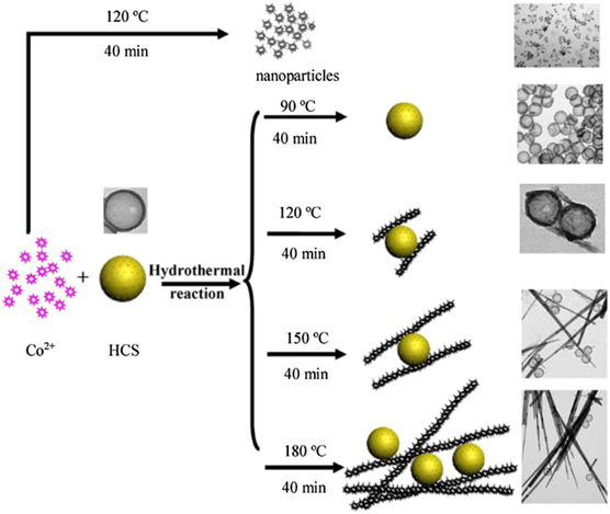
Figure 12. Schematic illustration for the growth mechanism of CoCH NWs-HCSs. Reprinted from [100], Copyright (2019), with permission from Elsevier.
Download figure:
Standard image High-resolution image10.2. Current and future challenges
On the whole, however, n-type MOS are actually preferred to be chosen as sensing substances than p-type MOS. As reported, the response of a p-type metal oxide to a specified gas equals the square root of that of an n-type metal oxide when the other parameters are almost the same [5]. Also, most reported Co3O4-based gas sensors usually operated at an elevated temperature above 200 °C. Therefore, the strategies of developing Co3O4-based gas sensors with lower working temperature is another focus area that researchers have already payed close attention to. Besides, although some achievements obtained, the response of Co3O4-based gas sensors is still relatively low and needs to be further enhanced.
We summarize the newest attempts for Co3O4-based gas sensors to overcome the above challenges as the major two kinds: composites with carbonaceous materials and derivates from MOFs. In recent years, low or even RM gas sensors based on MOS have aroused great interest of researchers. Except the assistance of catalytic action of noble metals, the composites consisting of MOS and carbonaceous materials are undoubtedly more adopted. As for Co3O4-based gas sensors, the addition of carbonaceous materials has markedly improved their sensing performance such as high working temperature.
Jung et al [98] fabricated hydrogen sensors through electrodepositing Co3O4 on CNTs-based sheets. After the annealing treatment, they found that the obtained CNTs/Co3O4 composite sensors exhibited a much higher response, shorter response and recovery times to hydrogen at RM than non-treated sensors. They contributed these improvements to the functional groups and oxygen defects formed during the annealing process that acted as chemisorption sites. They also deemed the good electrical conductivity of CNT crucial. Feng et al [99] reported the reduced graphene oxide (rGO) encapsulated Co3O4 NCs synthesized by the electrospinning technology. The as-prepared rGO/Co3O4 composite showed an excellent sensitivity and a fast response and recovery speed towards ammonia at RM. They speculated that the unique hierarchical wrapping microstructure, the selective NH3 adsorption sites at both the wrapping rGO layers and the polarized C–Co3+ covalent bonds were key factors. Zhang et al [100] successfully obtained the assembly of Co3O4 NWs and hollow carbon spheres (Co3O4 NWs-HCSs). In the sensing test, the Co3O4 NWs-HCSs showed the optimum operation temperature decreasing to 150 °C and could also exhibit high sensitivity to acetone at much lower working temperature of 75 °C.
For the synthesis of desired sensing materials, a facile and controllable method is always popular. In traditional ways such as electrostatic spinning and hydrothermal process, we have to undergo a torturous process in which countless parameters should be adjusted over and over before we eventually obtained the ideal products. In spite of this, the experiment could not be easily reproduced even we adopted the same procedure. Delightfully, the utilization of MOFs has successfully solved this problem, especially to Co3O4. As we know, ZIF-67 can be easily obtained through a coprecipitation process of cobalt salt and 2-methylimidazole in the solution of methanol. Also, the particle size of ZIF-67 can be regularly adjusted only through changing the addition amount of cobalt salt or 2-methylimidazole precursors. Besides, the synthesized regular dodecahedron of ZIF-67 can be approximatively regarded proportionable. A subsequent heat treatment of the self-sacrificial templates of ZIF-67 can result in the desired Co3O4 nanocages. Due to the elimination of functional linkers in ZIF-67, the obtained Co3O4 nanocages in this way are air-permeable and hierarchical, both of which are advantageous to their gas-sensing performance. Moreover, we can conveniently control the morphology of the obtained Co3O4 through changing the sintering parameters, such as atmosphere, heating rate, targeted temperature, duration time and so on.
For example, Zhang et al [101] successfully obtained four kinds of porous hierarchical Co3O4 structures by optimizing the thermal decomposition process using ZIF-67 as precursor. They considered that these novel Co3O4 structures with controllable channels, meso-/micropores and adjustable surface area are ideal candidates for gas sensing materials. Jo et al [102] prepared MOFs-derived hollow Co3O4 nanocages with tunable size and morphology through controlling the addition amount of 2-methylimidazole. In the sensing test, the sensor based on Co3O4 with the size of 1.0 μm exhibited not only ultrahigh responses to p-xylene but also a remarkably high selectivity to methylbenzene over the interference of ethanol. They attributed this to the highly gas-accessible morphology, abundant mesopores, high specific surface area as well as the high catalytic activity of Co3O4. They also regarded this method superior and indicative. Koo et al [103] obtained superfine PdO catalyst functionalized Co3O4 hollow nanocages with MOFs as templates (figure 13). Due to the restriction of cavity of ZIF-67, the size of Pd particles was confined to 2–3 nm. The Pd particles were separated uniformly in space at the same time. As a result, the elevated catalytic activity of PdO made the composites exhibit higher acetone sensing response.

Figure 13. Synthetic process of PdO–Co3O4 HNCs derived from Pd@ZIF-67 by optimized thermal treatment. Reprinted with permission from [103]. Copyright (2017) American Chemical Society.
Download figure:
Standard image High-resolution imageUp to now, we have summarized the challenges of Co3O4-based gas sensors and the solutions that researchers have taken to overcome them. To our pleasure, some positive improvements have occurred. However, we have to be aware of the consequent defects and surviving weakness. For example, under low or even RM, the response and recovery time of the sensors became very long, which severely restricted their practical application. Moreover, although the method of using MOFs as sacrifices is convenient and controllable, the gas-sensing performance of the obtained Co3O4 hollow nanocages is still dissatisfactory. All of these are the main challenges that researchers must try every means to conquer in the future.
Very recently, flexible and wearable gas sensors have shown a great potential, which have glamorous features and are promising in probable commercial applications. However, for Co3O4-based gas sensors, there rarely exist some related reports till now. For future research, we suggest some relevant studies on Co3O4-based gas sensors.
10.3. Concluding remarks
In the above sections, we established an all-around cognition about Co3O4-based gas sensors, such as the current research status, the research hotspots, challenges and some adopting means. We have witnessed some concrete progress and improvements, which were inspiring. However, the gas-sensing performance of Co3O4-based gas sensors is still relatively weak and there are still so many parameters needed to be promoted. Moreover, some newest trends such as flexible and wearable gas sensors have emerged recently. We also call for some innovatory attempts.
Acknowledgments
We acknowledge the support of the National Natural Science Foundation of China (61903159); Natural Science Foundation of Jiangsu Province (BK20190617) and the Fundamental Research Funds for the Central Universities (JUSRP11925).
11. V2O5 for gas sensors
A A Akande
University of Limpopo, South Africa
CSIR NextGen Enterprises and Institutions, South Africa
11.1. Status
Semiconducting metal oxide materials have dominated the field of gas sensing and air pollution detection for more than half a century now [104]. The history can be trace back to the work done at Bell Laboratory in 1950 on the modification of surface electrical property of Ge materials in different atmosphere [105]. Followed by several research works on ZnO, ZnO: doped/decorated materials in the 1960s and SnO2, SnO2: doped/decorated materials in the 1970s [104, 105]. Metal oxide gas sensors have recorded tremendous expansion in research between 1980s and 2020s with significant effort invested on investigating sensing properties of many oxides materials [104–106]. Vanadium pentoxide (V2O5) nanostructures has been mostly studied among its vanadium oxides counterparts for gas sensing application because of properties such as catalytic activities and layered structural property which makes it easy for the material to adsorb variety molecules on large surface area [107]. Alongside with its application in the field chemical and gas sensor, the material has also been well resaerched for lithium ion battery, catalysis, thermochromic and electrochromic applications. Owing to its excellent properties of fairly wide band gap, multiple valence, stable orthorhombic crystallographic structure (space group; Pmmn ( no. 59), lattice parameters; a = 3.563 Å, b = 4.369 Å and c = 11.510 Å) and good thermal stability [107].
Vanadium pentoxide NPs and thin film have been explored in the detection of many inorganic and volatile organic molecules. In 2015, Akande el al [108] reported higher selectivity of p-type V2O5 colloid nano-particles prepared by microwave irradiation of vanadium base precursor to NO2 than NH3 gas at 28 °C. The detection of NO2 was performed at 5–15 ppm which falls in the vicinity of the threshold limit value of NO2 reported by the Air Quality Control Ministry of Environment, Ontario, Canada. RM and low CH4 concentration detection of mixed phase V2O5:VO2 nano-spheres with large BET surface area and pore diameter was reported [109]. This sensor followed Langmuir adsorption model where the response increases exponentially with CH4 concentration before saturation effect at 40 ppm making it suitable for practical application. Furthermore, detection of many volatile organic vapours have been achieved using nanostructured flower like V2O5 thin film synthesized by spray pyrolysis [110]. This work showed that the RM sensing is highly selective towards xylen with short response and recovery time, the optical band gap of the material was also said to decrease with increase in the substrate temperature. Other report compared sensitivity of V2O5, VO2 (B) and VO2 (M) self-assembly nano flakes with V2O5 demonstrated superior sensing characteristics to 100 ppm of NH3 than VO2 (B) in terms of sensitivity, response time and reproducibility [111]. However, the VO2 (M) was found to be insensitive to the gas.
Gas sensor technology based on V2O5 material is highly important in gas sensing field for addressing the escalating environmental pollution and health problems because of its ability to detect gases at temperature near room. Unlike high band gap materials (e.g. TiO2, SnO2, ZnO etc), V2O5 possess relatively lower band gap energy property with high potential of detecting polar and non-polar molecules at room or relatively low temperature.
The future of V2O5 gas sensor would rely on intense research involving its combination with other materials either in the doping, composite, alloying or surface decoration/modification mode to enhance its sensing characteristics. Chimowa et al in 2017 attempted to improve the CH4 gas sensing properties of multi-walled carbon NTs by inserting or filling the tubes with V2O5 NPs [112]. The result showed significant increase in the sensitivity of vanadium oxide filled multi-walled CNT compared with unfilled NTs. Whereas, the sensitivity of the pure V2O5 is still far more superior to that of vanadium oxide filled multi-walled CNT. An ab initio calculation of electronic density of state was employed to verify the effect of vanadium oxides in the sensing properties of the multi-walled CNT. This calculation indicated that V2O5 been a semiconductor significantly increase the electronic state of the metallic multi-walled CNT thereby enhancing its gas sensing activity. However, the response and recovery times of both V2O5 filled and unfilled multi-walled CNTs are fairly good in comparison with the one of pure V2O5 sensor.
Another future prospect and advances of V2O5 based material lies in the development of optical gas sensing technology. Recently, Akande el al [113] advanced the field of optical gas sensing through the enhancement of 194 cm−1 phonon and shift of 996 cm−1 phonon of pulse laser deposited V2O5 thin film when exposed to NH3 molecule as shown in the figure 14. This result is considered as a step forward in addressing the poor selectivity of chemi-resistive metal oxide materials.
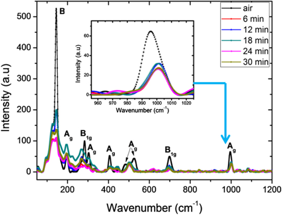
Figure 14. Raman spectra at 25 °C of V2O5 thin film in air, and covered with NH3 molecule recorded at 6 min intervals. The insert picture is the magnified images of 996 cm−1 Raman lines when the thin film is exposed to NH3 at 25 °C.
Download figure:
Standard image High-resolution image11.2. Current and future challenges
Despite the great potentials of V2O5 in developing practical and selective gas sensing technology, there are issues and challenges that would needs to be overcome to exploit its full benefit in the field. The major among these challenges is the multiple valence nature of vanadium as transition metal which often caused V2O5 to co-exist in phase (phase mixture) with other vanadium oxide members. Several authors have observed trace phases of vanadium oxide co-existing with V2O5 during gas sensing experiments which was reported to alter the gas sensing performance of V2O5. More so, figure 15 present depth profile analyse of pulse laser deposited V2O5 thin film which was carried out by time-of-flight secondary ion mass spectroscopy to unveil the species of the vanadium oxide present in the film. This profile showed co-existence of VO2 and V2O5 and their mixed valence structure V6O13 (this analysis is also supported by XPS). Other research issues are related to the poor selectivity and slow recovery ability (especially when in nano-size) which are also common challenges to the metal oxide gas sensor material's family in general.

Figure 15. (a) 3D overlays image of the entire V2O5 thin film displaying VO−, VO2 −, VO3 − as surface ions, (b) TOF-SIM depth profile of the negative ions of V, VO, Si and SiO2 species available in the V2O5 thin film.
Download figure:
Standard image High-resolution image11.3. Concluding remarks
This short review highlights the status, current and futures challenges of V2O5 material for gas sensing application. It presents the outstanding role which V2O5 have been playing towards building reliable gas sensing technology. It was said that the future prospect and contribution of V2O5 to the field of gas sensing lies in its phonon property which could be employed in the development of selective gas sensing technology. Finally, the study outlined the issue of multiple valence state of vanadium oxide as the major stumbling block towards harnessing the full gas sensing potential of V2O5 material.
Acknowledgments
AA acknowledge the National Research Foundation for the Innovation Post-Doctoral Fellowship Grant (Unique Grant No. 116749).
12. MoO3 for gas sensors
Arun K Prasad
Homi Bhabha National Institute, India
12.1. Status
MoO3 has been reported as a stand-alone gas sensing material as early as 1996 [114] where ammonia detection was shown in temperature range of 400–450 °C. The suitability to detect NO2 in temperature range from 200–400 °C in low concentration was demonstrated for the first time in 1998 [115]. The issue of selectivity towards ammonia with respect to nitrogen dioxides (the main interfering gas in selective catalytic reactors in diesel exhaust engines) and other gases have been addressed by Prasad et al in 2003 [116]. A mechanistic view contrary to the general gas sensing mechanism of oxygen chemisorption followed by reaction has been provided which shows that MoO3 undergoes reduction at the surface from Mo6+ to Mo5+ and Mo4+. This has led to extensive foray into mechanism-oriented research in MoO3. A guideline on polymorph selection to target a particular gas has been formulated based on results obtained with different iso-structural oxides including MoO3 [117, 118].
After the advent of nanotechnology-based sensors in early 2000s, much of the research in MoO3 has been re-inventing the wheel. Many researchers report the suitability of various shapes of MoO3 in nanostructure form for improved sensor response, reduction in operating temperature and enhanced selectivity. The focus of research gradually shifted towards synthesis of MoO3 in different nanostructures through various synthesis techniques with and without additives [119, 120]. But the understanding of the underlying sensing mechanism had stagnated.
The issues pertaining to optimizing the gas sensor performance with respect to MoO3 phase and microstructure are still relevant today. Addressing the mechanism of sensing has been mainly speculative. Simulations based on gas–material interactions combined with in situ experimental techniques to address the gas sensing mechanism in MoO3 is still in its primitive stage [121].
12.2. Current and future challenges
MoO3 is an n-type semiconductor with indirect band gap reported in the range from 2.7–3.2 eV. Stoichiometric MoO3 exists in 2 major forms viz, the stable α-phase which is orthorhombic with layered structure and metastable β-phase which has a ReO3-like structure [118]. The β-phase can transform into α-phase by glide along crystallographic shear planes. Apart from these two common phases, two more lesser known phases of MoO3 exist, viz, the hexagonal phase and the high pressure stabilized ε-phase [120]. These structures are depicted in figures 16(a)–(f). The basic unit is the MoO6 octahedra shown in figure 16(a). Almost all of the sensor research on MoO3 focuses on the stable α-phase. There are very few reports on gas sensing using other stoichiometric phases [119, 122]. Challenges and thereby opportunities lie in the stabilization of the phases for use in gas sensing. The presence of various sub-stoichiometric phases of MoO3 such as Mo18O52, Mo17O47, Mo9O26, Mo8O23, Mo5O14, and Mo4O11 further complicate the understanding of sensing process.

Figure 16. (a) MoO6 octahedra composed of molybdenum and oxygen atoms. (b) Thermodynamically stable orthorhombic α-MoO3 with layered structure held together by van der Waals' forces. (c) Metastable monoclinic β-MoO3. (d) ε-MoO3, also known as MoO3-II. (e) Metastable h-MoO3. (f) Tunnel structure along the c-axis of h-MoO3. [120] John Wiley & Sons. [Copyright © 2017 WILEY‐VCH Verlag GmbH & Co. KGaA, Weinheim].
Download figure:
Standard image High-resolution imageThe operating temperature with MoO3 remains a challenge due to its relatively lower melting point of 795 °C. It shows excellent sensor properties around 400–500 °C above which the sensor property deteriorates due to volatilization. This limits its use in harsh environments like automotive exhausts on a prolonged basis. But the size reduction to nano-dimensions have helped in reducing the operating temperature in the region of 100–350 °C [123]. This greatly enhances its utility in low power devices for domestic and industrial applications.
Currently there is abundant literature on different shapes of nanostructured MoO3 being used in gas sensing. A comparison of several nanostructures of MoO3 with important sensor parameters is given in table 1. As is observed, several processing techniques are utilized leading to varying morphology. And there is absence of a trend which relates the structure to particular preference towards gas sensing. A common measurable parameter such as surface area, mobility, defect concentration etc has to be provided which can be correlated with sensor response to derive a meaningful inference. This will also help in identifying the dominating parameter in the sensor behaviour.
Table 1. Comparison of sensing parameters of several MoO3 based nanostructures in last decade.
| Material | Synthesis | Morphology | Gas | Conc. (ppm) | Operating temp. (°C) | Ra/Rg | Year | Reference |
|---|---|---|---|---|---|---|---|---|
| MoO3 | Ultrasonic | Nanorod | NO2 | 10–500 | 290 | 542 | 2012 | [119] |
| MoO3 | Spray pyrolysis | Nanolamellae | Tri methyl amine | 0.1–100 | RT | 12 | 2014 | [124] |
| MoO3 | Solvothermal | Nanoflower | Triethyl amine | 0.5–100 | 250–370 | 416 | 2015 | [125] |
| MoO3 | Chemical methods | Nanosheet | Ethanol | 10–500 | 175–350 | 33 | 2016 | [126] |
| MoO3 | Hydrothermal | Nanobelts | Tri methyl amine | 1–50 | 100–380 | 582 | 2016 | [127] |
| MoO3 | Electron beam | Nanobelts | H2S | 1–100 | RT-327 | 225 | 2016 | [128] |
| evaporation | ||||||||
| MoO3 | Chemical methods | Nanoplates | Xylene | 10–1000 | 260–400 | 87 | 2017 | [129] |
| MoO3–SnO2 | Chemical methods | Nanofibers | CO | 50–300 | 200–400 | 2.4 | 2017 | [130] |
| MoO3/Fe2 | Hydrothermal | Nanoparticle on | Toluene | 10–50 | 150–350 | 5.3 | 2017 | [131] |
| (MoO4)3 | nanobelts | |||||||
| MoO3 | Spray pyrolysis | Nanobelts | NO2 | 20–100 | 150–250 | 68 | 2017 | [132] |
| Pd–MoO3 | Spray pyrolysis | Nanobelts | NO2 | 5–120 | 100–250 | 95.3 | 2018 | [133] |
| MoO3 | Hydrothermal | Nanoflower | Ethanol | 50–400 | 50–350 | 50 | 2019 | [134] |
| MoO3 | Hydrothermal | Nanorod | Triethyl amine | 0.1–100 | 100–350 | 153 | 2019 | [123] |
| Ni–MoO3 | Solvothermal | Nanopompon | Xylene | 1–100 | 175–325 | 62.5 | 2019 | [135] |
| Zn–MoO3 | Solvothermal | Nanoflower | CO | 1–200 | 120–380 | 50 | 2020 | [136] |
Though there is scope in adding additives/dopants/binary oxides to extract a desired response, especially selectivity, single phase MoO3 lends itself to flexibility through its crystallographic phases, sub-stoichiometric oxides, defects through Ov which can be utilized to meet the demands of good sensing material. However, in order to decipher the link between structure and properties, some literature needs to be borrowed from other areas such as catalysis, thermodynamics [120], DFT calculations [121] and charge transfer kinetics into gas sensing research. Exploration of defects in MoO3 have to be pursued with advanced techniques such as photoluminescence, positron annihilation spectroscopy, deep level transient spectroscopy etc. In situ characterization like XPS, evolved gas analysis, Raman spectroscopy, FTIR needs to be conducted to understand the surface phenomenon during gas sensing. The future challenge lies in categorizing microstructural properties (morphology, shape, size, crystal structure), electronic properties (mobility, charge carrier concentration, defects) and establish their effect on sensing. As with any metal oxide gas sensor, to be used in commercial sensors, the conditions for detecting of a particular target gas using MoO3 has to be specified which should be independent of shape or size/dimension. It should also be feasible to synthesize such material in large scale on a reproducible basis. Efforts towards such focussed characterization will yield large scale commercial sensor based on MoO3.
12.3. Concluding remarks
Molybdenum trioxide has been shown as an excellent gas sensing material to detect a variety of gases for the last two decades. Focus in first decade remained on the variety of synthesis techniques and gases that could be detected with minimal focus on mechanistic studies. Subsequently, focus shifted on synthesis of different nanostructure morphologies and exploration of gas sensing mechanism by electrical and spectroscopic studies. Current trend in supporting gas sensing with advanced techniques of in situ characterization is highly encouraging and will help in tailoring single-phase nanostructure/bulk MoO3 to achieve desired sensing property.
Acknowledgments
The author thanks Prof. Perena Gouma (presently at Ohio State University, USA) and Dr David Kubinski (Ford Scientific Research Labs, Dearborn MI, USA) for discussions on molybdenum trioxide and their utility in gas sensing.
13. In2O3 for gas sensors
Mara Bruzzi
University of Florence, Italy
13.1. Status
Indium oxide (In2O3) is a semiconductor material with a broad direct band gap of 3.55–3.75 eV and an indirect energy gap of 2.62 eV [137]. It is characterized by a complex cubic bixbyte structure originating from an array of unoccupied tetrahedral oxygen anion sites. Its n-type nature is due to the deviations from stoichiometric composition, either the excess indium atoms or Ov. Serving as donors, they are responsible for electronic conductivity [138]. As for other metal oxide sensor materials, its gas sensing properties are based on chemical interactions between ambient gas molecules and surface. Processes controlling the rate of conductivity response of In2O3 thin film sensors to both reducing and oxidizing gases have been widely reviewed in past [139]. Chemical adsorption of oxygen species creates extrinsic acceptor states, generating an electron depletion layer in the region near surface. In granular systems, these depletion layers create Schottky barriers between grains. In recent years, indium oxide has shown its strong potential as a material for gas sensing mainly due to its high electrical conductivity, high chemical stability and high sensitivity. In general, high sensitivities and fast response rates are achieved by increasing the surface-to-volume ratio. Therefore, growth processes are mainly focussed on In2O3 NSs as NTs, NWs, NPs, NSHs. In past, In2O3 nano-structured sensors have been manufactured by many different techniques such as CVD, thermal oxidation of films, spray pyrolysis, sol–gel, atomic layer deposition (ALD), pulsed laser ablation, DC, and RF-sputtering. These techniques generally require a complex processing for precursors to be formed in the environment of the deposition chamber. Further, they need rather high temperatures of the substrate, and generally do not allow for using substrates already equipped with screen printed circuitry, as is the case of gas sensing devices, which will be damaged or even melted by high temperatures. In [140] nano-crystalline layers of In2O3 have been deposited directly on dedicated printed circuit boards (PCBs) by low temperature pulsed electron deposition (LPED). This technique allows for depositing homogeneous films with the proper stoichiometry of almost any kind of materials at low temperatures, so that direct deposition on temperature-sensitive substrates as PCBs is possible. As an example, figure 17(a) shows a thin In2O3 film deposited by LPED on an alumina PCB equipped with interdigitated contacts for gas sensing and a Pt sensor for temperature measurement. During growth, both temperature and resistance of the film, are monitored, this latter show an exponential decrease as a function of the deposition time (figure 17(b)). By opportunely selecting deposition rates and times, this remote monitoring allows for tailoring in situ the optimal resistance and thus controlling sensitivity of the film. Sensing performance of In2O3 can be promoted through CS and spillover effect by adding catalysts metals such as Au [141], Pt, Pd [142]. Ionsorptions of oxygen ions occur on the metal nanoparticle surface due to the highly conductive nature and availability of free electrons. Then, the as created activated oxygen species are spilled onto the MOS surface and interact with the absorbed oxygen. This process results in greater and faster reactions between analytic molecules and adsorbed oxygen. Generally, at low temperature most semiconductor MOS are insulators rather than semiconductor, thus their gas sensing sensitivity is low. After the introduction of metal, ionsorption of oxygen ions can occur on the metal surface even at RM due to the highly conductive nature, availability of free electrons, and CS. Further, the metal–In2O3 interaction leads to a modification of the surface electronic structure. However, the gas sensing performance can be limited because of strong agglomeration during the synthesis process. To avoid this, metal loading has been applied to a variety of ordered meso- and macro-porous In2O3 nanostructures. Porous nanomaterials, e.g. obtained by employing colloidal crystals as the template, not only facilitate gas diffusion but also provide larger surfaces. The sensitivity is increased also due to the cooperative effect between Ov and grain boundaries potential barriers induced by means of hierarchical porous architectures [142]. Recently, the research has moved towards three-dimensionally ordered meso- and macro-porous nanomaterials, which can provide stable structures with higher surface-to-volume ratios. As an example Pd loaded in three dimensionally ordered macroporous (3DOM) In2O3 sensors have been synthesized by loading Pd NPs onto 3DOM In2O3 using NaBH4 as reducing agents [143]. Enhanced NO2 sensing performance is explained in terms of Pd functionalization inducing an electronic state change on the 3DOM In2O3 surface, and of the correspondingly increased thickness of the depletion layer. The modification of the surface electronic structure can be realized also by means of heterojunction nanocomposites involving foreing metal oxide nanostructures interfacing In2O3. These composite systems achieve enhanced sensitivities by profiting of the synergistic effects between the two different MOS as well as due to the influence of microstructural and compositional effects. As an example, the response to acetone has been increased using hollow sphere composites synthesized by a template-free hydrothermal method from MoO3 and In2O3 [144]. The spheres have a typical size of 800 nm, when exposed to 100 ppm acetone at 250 °C, response is 13.6 times higher than when using pure MoO3.
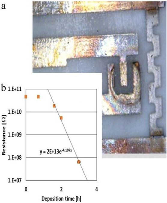
Figure 17. (a) In2O3 thin film deposited by LPED at Florence University directly on alumina substrate equipped with interdigitated contacts for gas sensing and Pt temperature sensor T = 60.57 ± 4.03 °C. (b) Electrical resistance measured in situ during time of growth of the In2O3 thin film, showing exponential decrease of film resistance during growth.
Download figure:
Standard image High-resolution image13.2. Current and future challenges
Metal oxide semiconductor gas sensors are increasingly used in industrial production and daily life, favoured by their outstanding physical and chemical properties, low cost and simple preparation methods. A variety of In2O3 hybrid nanostructured sensors showed promising results under exposure to various VOCs and toxic gases, such as NO2, acetone, formaldehyde [145], as well as ethanol, CO, acetaldehyde, and their practical applications could be foreseen in near future. Current challenges concern the achievement of ultrahigh sensitivity, as well as reduction of operating temperature and recovery times. In this respect, excellent results have been achieved for some toxic gases using ordered porous In2O3 structures loaded by metal NPs. As an example, Pd loading in macroporous In2O3 structures allowed for a ppb-level NO2 detection at RM, providing an efficient approach detection without extra heating. Further, In2O3 hierarchical architectures exhibit excellent formaldehyde (HCHO) sensing performances with rapid response/recovery behaviour (1 s/8 s), good selectivity and favorable stability for 100 ppm at 260 °C. Future challenges mainly concern the achievement of such promising sensing performances for a broader spectrum of toxic gases. Further, gas selectivity in the presence of other adsorbing gases still need progressing. Promising results have been achieved in this respect, as an example, by using In2O3 hollow nanostructures (HMs) synthesized by a facile route with low-cost yeast as a bio-template [146]. Tests showed excellent selectivity for chlorine (Cl2) relative to NO2 and other diverse VOCs.
Ultra-high sensitivity, low temperature operation and increased selectivity of In2O3 gas sensors will open the way to their application also in medical diagnostics. As an example, selective detection of specific VOCs can be used to evaluate biomarkers in exhaled breath from the metabolism process. In particular, detection of acetone in human exhaled breath plays an important role in the diagnosis of diabetes. However, obtaining a reliable response to ppb levels of acetone avoiding cross-sensitivity due to the large amount of moisture in exhaled breath is still a challenge.
Future challenges have to focus on the development of facile and low-cost manufacturing technologies allowing for increasing functionality of the In2O3 sensors. In this respect, manufacturing nanostructured In2O3 directly on PCBs while remotely controlling the sensor electrical parameters in situ during the growth process should be regarded as a promising route, as it should allow for an optimal tailoring of the sensing properties of the whole device.
Finally, an open and stimulating frontier for In2O3 sensors regards their integration with wireless operation systems in view to their application in large-scale frameworks as next-generation automotive and wearable electronics.
13.3. Concluding remarks
Being characterized by a high electrical conductivity, chemical stability and sensitivity In2O3 is a promising material for gas sensing. A variety of In2O3 hybrid nanostructured sensors showed promising results under various VOCs and toxic gases. In particular, metal loading in In2O3 meso-porous structures and heterojunction nanocomposites, allowing for modification of the surface electronic structure and profiting of synergistic effects, resulted in enhanced sensitivities down to the ppb-level detection, even at RM. Future challenges concern mainly increasing selectivity towards different gas species, development of manufacturing methods allowing for controlling the optimal characteristics of the whole sensing device, integration with wireless operation systems for large scale applications.
14. ZnFe2O4 for gas sensors
Kaidi Wu and Chao Zhang
Yangzhou University, People's Republic of China
14.1. Status
Owing to simple operation, easy integration and low cost compared with other technologies (e.g., colorimeter, chromatography), gas sensors have been considered as an effective technique to monitor atmospheric gas emissions and detect flammable, explosive or toxic gases in industrial production or household use. Binary metal oxide semiconductors based on gas sensing materials, e.g. ZnO, SnO2, In2O3 and WO3, have been intensively studied and applied in the detection of H2, NO2 or NH3 [147]. However, their sensing properties still face a lot of limitations such as limited detection range, poor selectivity and low stability. In order to develop high-performance gas sensors, it is vital to discover novel and cost-effective sensing materials. As an emerging ternary metal oxide semiconductor, zinc ferrite (ZnFe2O4) is a typical normal spinel structure material (AB2O4) which has been widely studied and applied in electromagnetism, catalyst and other fields. As shown in figure 18, the unit cell of ZnFe2O4 is an array of face-centered cubic oxygen anions (O2−), in which Zn2+ occupies the tetrahedral interstices formed of O2− and Fe3+ occupies octahedral interstices formed of O2−. Hence, ZnFe2O4 exhibits excellent physical and chemical properties.
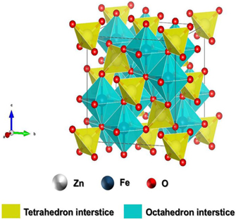
Figure 18. Schematic diagram of face-centred cubic ZnFe2O4.
Download figure:
Standard image High-resolution imageNanostructured ZnFe2O4 possesses a narrow bandgap (around 1.9 eV), which was first reported as gas sensing material in 1999, showing high response and selectivity to ethanol [148]. In the past two decades, several enhancement strategies for ZnFe2O4-based gas sensors have been developed to realize rapid tracking of target gases. Since the sensing performance of resistance-type ZnFe2O4 gas sensor is influenced by the surface gas–solid phase reaction process, the fabrication of novel microstructure/nanostructure affects interface adsorption sites and reaction zone of ZnFe2O4 nanomaterials, thus improving the gas sensing performance. Qu et al [149] reported a comparison among ZnFe2O4 spheres with different nanostructures, and the results showed that the double-shell materials displayed larger specific surface area, better crystallinity and significantly enhanced sensing properties compared to yolk–shell and solid spheres. The metal-doped ZnFe2O4 gains more surface activation energy and enhances the response to low concentration target gases, while retaining the original crystal structure. For example, Zhang et al [150] modified ZnFe2O4 with Ag NPs to obtain fine sub-ppm acetone sensing properties. In addition, Wu et al [151] utilized p-type rGO to strengthen ZnFe2O4 electronic properties resulting from the p–n heterostructure. Constructing homo/hetero-junction is also an effective approach to enhance the electronic properties of gas sensors, which utilize the interface synergic effect between materials with different bandgaps. It can be concluded that proper adjustment of micro/nanostructure, doping elements with appropriate ratio and composition with other semiconductors can contribute to improving the performance of ZnFe2O4-based gas sensors.
With the increasing awareness of human health, the demand for rapid clinical diagnosis has attracted much attention. According to the literature, analysis of the featured VOCs concentration in exhaled breath, a potential biomarker for certain diseases, will be a novel rapid and nondestructive diagnosis strategy, for example, acetone for diabetes, ammonia for chronic kidney disease [152]. Portable gas sensors can promote non-invasive, convenient, cost-effective, and efficient clinical monitoring. Thanks to its high response, long-term stability and safety, ZnFe2O4-based gas sensing material is a promising candidate for exhaled breath gas detection.
14.2. Current and future challenges
There are two main challenges faced by ZnFe2O4 gas sensors in disease detection. The first is that the concentration of the target gas in the respiratory gas is usually very low. There is a high requirement for the detection limit of the selected sensor material and response to the target gas under working conditions. Second, since the components in the human exhaled gas are extremely complex, and the determination of whether the detection object has a corresponding disease depends on the concentration of several of the marker gases, the sensor needs to be highly selective for the target gas. Hence, new modification strategies have been proposed.
On the basis of surface conduction mechanism, introducing Ov in ZnFe2O4 may be a novel point to modify electronic and gas sensing properties. Peng et al [153] induced the occurrence of Ov in ZnFe2O4 NPs via oxidation catalysed treatment, which behaved superior acetone sensing properties. Ov plays an electron donor role in n-type semiconductor, which narrows the bandgap and improves the adsorption efficiency of oxygen species. The essential reason for the narrowing of the semiconductor bandgap caused by the introduction of Ov is that the top of the VB shifts up and the VB widens. And the effect on adsorption process can be explained as follows: the introduction of Ov increases the electron concentration, and allows the gas molecules to capture electrons from ZnFe2O4 surface easily. Due to the increased number of electrons transferring between ZnFe2O4 and gas, the chemical adsorption of the gas is enhanced, as well as the response of the sensor. Moreover, the rich Ov self-doping will also accelerate the electron transmission speed, which contributes to improving the surface adsorption and desorption speed of sensors. However, there still exist limitations in the synthesis methods of semiconductor materials with rich Ov. As for direct synthesis method, the growth speed of crystals is relatively slow, and the surface of products has fewer oxygen defects. The post-treatment methods such as chemical reagent reduction, electrochemical reduction, high-temperature reduction, etc, require at least two steps to produce Ov, and the preparation process is complicated with a limited efficiency.
Due to the difference in the geometric shape, ionic bond energy between the cations (occupying octahedron and tetrahedron sites) and the surrounding oxygen ions, the physical and chemical properties of spinel ferrite are highly dependent on the composition, charge state or cations arrangement. Therefore, redistributing metal cations in spinel ferrites brings new possibilities to gas sensing material design. As one innovative reinforcement method, the role of substitution on crystal characteristic, magnetism and electron excitation properties of Mx Zn1−x Fe2O4 (M = Ni, Mn, Mg, Co, etc) has been widely investigated. The sensitivity and selectivity of mixed ferrites sensors were improved [154]. However, the detection limitation needs to be further reduced. Due to the different ionic radius of cations, the crystal characteristic of mixed ferrite may be changed, resulting in the generation of Ov or electron hopping in the lattice. Hence, combing the redistribution of cations and introduction of Ov may be a promising approach to obtaining excellent sensing properties of ZnFe2O4-based materials.
14.3. Concluding remarks
With continued development, ZnFe2O4-based gas sensing materials show promising interest in industrial and clinical diagnosis fields. ZnFe2O4-based materials can provide high response, selectivity, and long-term stability using the above-discussed strategies: tailoring nanostructure, element doping, constructing homo/heterojunction, inducing Ov and cations redistribution. However, there are still challenges in practical application such as high operating temperature, low recovery speed and poor independence with humidity. For further development of ZnFe2O4-based gas sensing materials, new strategies and corresponding influence mechanisms should be studied. Some pioneering work has been done, for example, Zhai et al [155] prepared metal–organic frameworks (MOF)–ZnO/ZnFe2O4 via a self-template method, and it behaved a fast response/recovery to triethylamine at a low operating temperature. Li et al [156] reported Au–ZnO/ZnFe2O4 multi-components nanomaterials prepared via electrospinning and ALD technique for ppb level acetone sensor. Hence, the combination of multiple enhancement strategies deserves further study. Moreover, inspired by the researches on ZnO and Fe2O3-based gas sensor under the assistance of UV or visible light illumination at RM, ZnFe2O4 with narrow bandgap may also benefit from light illumination. From a kinetic point of view, it is similar to heating, photon energy will be converted to electron transition energy, which will also improve the electron concentration and accelerate the rate of gas–solid phase reaction. Hence, utilizing light with favourable wavelength to illuminate ZnFe2O4-based sensing materials may be a novel research direction. In conclusion, future researches should be focussed on the rapid fabrication, composition design and mechanism understanding of ZnFe2O4-based sensing materials.
Acknowledgments
This work is financially supported by the National Key R&D Programme of China under Grant No. 2017YFE0115900 and Natural Science Foundation of China under Grant No. 51872254.
15. MoS2 for gas sensors
Rahul Kumar and Mahesh Kumar
Indian Institute of Technology Jodhpur, India
15.1. Status
Detection of single gas molecules at RM by using graphene sensor in 2007 has been aroused immense interest in the exploitation of 2D materials in gas sensing applications [157]. Analogous to graphene, a 2D semiconducting MoS2 with tunable bandgap, being the frontrunner of layered transition metal dichalcogenides (TMDCs) family, has shown great potential in gas sensing field as a result of its high surface-to-volume ratio, availability of most vibrant adsorption sites (sulphur vacancy, defects, and edge sites), and superb physicochemical properties. Stacking of the MoS2 layers with weak van der Waals force assists easily to exfoliate into a single layer. An exfoliated single layer of MoS2 did not show a response to gas due to unstable current over the time. However, five layers of MoS2 exhibited high sensitivity to gas at RM without any extra energy source such as temperature or light source (figure 19) [158]. Detection of gases at RM is attributed to charge transfer mechanism through electronics interaction between gas molecules and adsorption sites on MoS2. This room-temperature operation removes the microheater from conventional solid-state gas sensor technology which also helps to develop a miniaturized battery operated gas sensor for advanced internet of things applications.

Figure 19. (a) Schematic diagram of MoS2 gas sensor. (b) Photograph of MoS2 sensor device mounted on the chip. (c) SEM image of mechanically exfoliated MoS2 based device. (d) Comparative sensing performance for 2 and 5 layers MoS2 to 100, 200, 500, 1000 ppm NO2. Reprinted with permission from [158]. Copyright (2013) American Chemical Society.
Download figure:
Standard image High-resolution imageGas sensitivity of the MoS2 gas sensor could be improved via two ways: (1) to modulate the Schottky barrier height or width at an interface of metal electrode and MoS2 sensing layer under exposure to gas, (2) to increase most vibrant reactive sites through modification of MoS2 sensing layer. A Schottky contacted MoS2 gas sensor exhibited high sensitivity with detection to 20 ppb NO2 at RM [159]. MoS2 sensing layer in terms of vertically aligned flakes, NWs and flower nanostructure exhibited higher gas sensitivity than that of horizontally aligned MoS2 due to having more edge sites. Because, high d orbital electron density as well as more dangling bonds at edge sites of MoS2 help to strong gas adsorption, however, basal plane sites are chemically inert with no dangling bonds. Moreover, MoS2 NSs network with higher edge sites-to-volume ratio showed a very low detection limit to 4.2 ppb NO2 at RM [160]. Furthermore, defects engineering in terms of created sulphur vacancy and interface engineering in terms of surface functionalization improved the sensing performance of the MoS2 through chemical and ES [161]. In addition, high flexibility (high strain up to 11%) and excellent transparency of the MoS2 were utilized for developing a flexible and wearable gas sensor. Non-centrosymmetric structure of monolayer MoS2 due to absence of inversion centre induces piezotronics effects, which was exploited to enhancing the gas response of flexible MoS2 gas sensor. Strain induces pizocharges at MoS2/electrode interface and these piezocharges assist to improve sensitivity through modulating the Schottky barrier height or width [162].
15.2. Current and future challenges
Despite the detection of gases at RM with high sensitivity, there are some crucial challenges and concerns which create obstacle in the path of MoS2 gas sensing field for bringing it towards commercialization. Layered MoS2 changes its sensing characteristics according to its number of layers. Four or five layers MoS2 based gas sensor exhibited higher gas sensitivity than single or two layers MoS2 [158]. So, this is still an issue to clarifying the sensing behaviour of the MoS2 on the number of layers' perspective. Moreover, slow response and recovery kinetics of the MoS2 gas sensor at RM are the main challenges. Pristine MoS2 sensor exhibits a slow response time of approximate 3–4 min and recovery time more than 10 min at RM [163]. During the desorption process, energy at RM is not sufficient to break strong interaction of gas molecules (NO2, NH3) from adsorption sites of MoS2, therefore it shows incomplete recovery at RM. In addition, selectivity is also a challenge because MoS2 shows a gas response to different gases at RM.
To date, gas sensing mechanism of the MoS2 gas sensor is not clear, mostly researchers describe the sensing mechanism based on charge transfer in between gas molecules and different adsorption sites of MoS2. This charge transfer changes directly carriers concentration of the MoS2, thereby, resistance/conductance of the sensing layer changes. However, few researchers explain the change in resistance/conductance of the MoS2 based on the chemical interaction of gas molecules with adsorbed oxygen ions on MoS2 sensing surface. Similar to the sensing mechanism, there is also a dilemma in stability of the MoS2 sensor in air ambient. Mostly gas sensing experiments were performed in inert ambient (Ar or N2 gas) because the MoS2 gas sensor shows unstable sensing response in air ambient at RM, however, few reports also showed stable gas response in an air atmosphere. Metal oxide SnO2 NPs were incorporated in MoS2 for producing a stable response in air ambient at RM [164]. Thus, these are some concerns which should be resolved to understand the exact gas sensing mechanism and stability of the MoS2 gas sensor.
The sensing performance of hybrids, nanocomposites, and van der Waals heterostructures of MoS2 was improved with the contribution of a synergistic effect of chemical and electronics sensitization. However, the exact contribution of individual material in gas sensing is still not clear. So, this is a challenge to select a particular material for incorporating into MoS2 to improve specific gas sensing characteristic for a desired application. Moreover, a simple, robust and advance synthesis process is still a challenge for fabricating MoS2 van der Waals heterostructures because precise control and proper alignment of the material position are required for fabricating van der Waals heterostructures.
There are some challenges for a reliable large-scale growth of the MoS2 and production of gas sensors at the industry level. Currently, a simple wet-chemical process is being used for fabricating the individual MoS2 or its nanocomposites-based gas sensors at rigid as well as flexible substrates. However, this solution process restricts to explore the intrinsic gas sensing characteristic of the MoS2 due to adding impurity during the synthesis process. Physical and CVD methods are also being developed for synthesizing large scale MoS2 for developing gas sensors. Nonetheless, there is a long journey for reaching at industry level or integrating with existing technology.
Extra energy sources (temperature or UV-light) are being used to address slow response/recovery kinetics of the MoS2 gas sensor. Thermal energy is capable to achieve complete recovery through providing energy above the threshold energy to adsorbed molecules and it also improves the response time. However, the gas sensitivity is severely deteriorated with increased temperature due to higher desorption rate than the adsorption rate. Moreover, the UV light source helped to achieve fast response and recovery time with increased gas sensitivity at RM7. However, integration of extra heating element or light source with MoS2 gas sensor limits it to make better from commercial metal oxide gas sensor technology.
The selectivity of the MoS2 gas sensor was improved by functionalizing the MoS2 via metal or metal-oxide-semiconductor nanoparticle as well as incorporating another material into MoS2. With the emergence of van der Waals heterostructures of the 2D materials in gas sensing, MoS2 integration with another material with different band structure or workfunction in terms of van der Waals heterostructure would be more useful in the context of reliable selectivity as well as excellent sensitivity. The selectivity of the sensor could be enhanced via a selection of materials with particular gas molecules adsorption capability. In addition, in order to find the exact contribution of heterojunction area of two 2D-materials in gas sensing, graphene/MoS2 van der Waals heterostructure was demonstrated for NO2 gas at RM. In this device, all parts were passivated by gas barrier layers except graphene/MoS2 heterojunction (figure 20) and this heterojunction exhibited a change in resistance by a factor of greater than 103 to 1 ppm NO2 [165]. On the other hand, flexible MoS2 gas sensor in its nascent stage, therefore a lot of outcomes and results are still waiting for utilization of the MoS2 in emerging flexible and wearable gas sensing field.
Figure 20. (a) Schematic diagram and (b) optical microscope images of MoS2 and graphene van der Waals heterostructure based gas sensor device. Reprinted with permission from [165]. Copyright (2018) American Chemical Society.
Download figure:
Standard image High-resolution image15.3. Concluding remarks and prospects
Detection of gas molecules at RM without any extra energy source have stimulated the enormous interest in 2D MoS2 for gas sensing application. This field of MoS2 gas sensor is rapidly growing and emerging towards a possibility of commercial acceptance. Besides the huge potential and rapid growth of MoS2 in gas sensing field, there is a still a gap between the laboratory's research and industry. So, many multidisciplinary research efforts are also required for MoS2 gas sensing research to move towards a commercial product.
Acknowledgments
We acknowledge the support by Science & Engineering Research Board (Sanction order No. CRG/2019/000112).
16. WS2 for gas sensors
Youngjun Kim
Yonsei University, Republic of Korea
16.1. Status
WS2 is being researched as a chemiresistive gas sensor materials, which is one of various transition metal chalcogenides (TMD) material along with MoS2 [166–169]. Compared to gas sensor based on oxide materials, it has higher responsivity to gas sensing at RM [166, 167, 170]. Therefore, it has the potential to reduce the power consumption and gas sensor size in the future. In order to secure the selectivity for the gas, which is a weakness in the semiconductor gas sensor, measurements on various gases have been carried out. The results of the experiments to date suggest that the WS2 gas sensor has selectivity for NO2 [166, 167].
The reason for the active study of WS2 gas sensor with these advantages is related to the synthesis methods. Large area synthesis is an essential process for the application of WS2 material as gas sensor. Among the various methods, the development of WS2 synthesis based on CVD and ALD, which have advantages in large area uniformity with layer number controllability, was important step for the WS2 gas sensor study [171, 172]. In case of WS2 synthesized on the basis of ALD process, it was found that the responsivity of NO2 increased as the number of WS2 layers increased (figure 21(a)) [166]. However, since the responsivity values between NO2 and acetone gas in the pristine WS2 gas sensor were similar, the responsivity for each gas needed to be more clearly distinguished.

Figure 21. (a) NO2 and acetone sensing response of pristine WS2 and Ag NW functionalized WS2 (b) recovery characteristic of pristine WS2 and Ag NW functionalized WS2 in NO2 sensing. Reprinted with permission from [166]. Copyright (2016) American Chemical Society.
Download figure:
Standard image High-resolution imageFor enhancing the NO2 responsivity of a WS2 gas sensor, Ag NWs (NW) were functionalized on the WS2 surface, in the same way as the metal functionalized in the oxide-based semiconductor gas sensor. The responsivity to NO2 gas increased by more than 10 times in Ag NWs functionalized (ANF) WS2 gas sensor compared to pristine WS2, resulting in improved gas responsivity. On the other hand, the responsivity to acetone gas was reduced in the ANF WS2 gas sensor, indicating that the selectivity to NO2 gas was more clearly obtained. The representative performance indicators of typical gas sensors include recovery in addition to responsivity and gas selectivity. The recovery after the gas reaction is related to the reliability of gas sensor. In the case of pristine WS2, there was poor recovery characteristic of NO2 under 100 ppm. On the other hand, recovery of NO2 gas in ANF WS2 gas sensor significantly improved with greater than 90% which results from the catalytic effect and n-type doping effect of Ag nanowire (figure 21(b)). This approach has been ongoing in other TMD material, Pt NPs functionalized MoS2 gas sensor, for improving the responsivity of NH3 and H2S gas [173]. The functionalization of various kinds of metals into WS2 materials is expected to improve the responsivity and recovery characteristics of WS2 gas sensor as well as to secure the selectivity for specific gas.
In addition to functionalization using metals to increase the responsivity of the WS2 gas sensor, there was study in other approach using a WS2x Se2−2x alloy in which a part of the sulphur of WS2 is substituted with selenium for enhancing the NO2 responsivity [167]. In WS2x Se2−2x alloy gas sensor, about 2–5 times enhanced responsivity to NO2 gas (50–500 ppm) better than WS2 gas sensor (figure 22(a)). This study suggested two assumptions for this result. One is that the WS2x Se2−2x alloy material had a lower carrier concentration than that of WS2, which means that the NO2 molecule induced a larger carrier concentration change in WS2x Se2−2x alloy. The other assumption was the difference in charge transfer and adsorption energy between the NO2 gas and each 2D TMD surface. Through this research, alloying or doping with other elements are expected to improve the responsivity of the WS2 gas sensor.

Figure 22. (a) Response of WS2, WSe2 and WS2x Se2−2x alloy for NO2 gas (b) NO2 gas sensing of the flexible WS2x Se2−2x alloy gas sensor before and after bending test. Reprinted with permission from [167]. Copyright (2018) American Chemical Society.
Download figure:
Standard image High-resolution imageThe fact that the WS2 applied to flexible substrates due to the atomically thin thickness is the background that the research on WS2 gas sensor continuously interested along with its gas sensing characteristics. By transferring the WS2x Se2−2x on polyethylene terephthalate substrate, it was confirmed that the responsivity of NO2 gas increased even after 5000 time of bending (figure 22(b)). The reason could be related to the defect site generated during the bending process which acted as the adsorption site for NO2 gas. Accordingly, it is anticipated that the study on large area transfer method along with low temperature WS2 synthesis method for applying WS2 to flexible gas sensor.
16.2. Current and future challenges
Although the WS2 gas sensor has the advantages described above, there are other factors that need further challenges. The following points are introduced based on the results of the previously reported WS2 gas sensor and other TMD gas sensor (e.g. MoS2 gas sensor with similar characteristics to WS2 gas sensor).
First of all, it is essential to study the correlation between contact resistance and gas sensor performance in WS2 gas sensor. In the case of transistors, a variety of studies for reducing the contact resistance between the TMD material and electrode in order to improve the mobility and the on/off ratio are still actively studied. However, there are few studies on contact resistance in WS2 gas sensor. In MoS2 gas sensor, it was reported that the responsivity of NO2 increased when the electrode with higher Schottky barrier was used. In addition, for CO gas, the presence or absence of responsivity was observed depending on the electrode type. These suggest that the Schottky contact could change the responsivity and selectivity for gas in WS2 gas sensor. In addition to using various kinds of electrodes, considerations such as contact structures, tunnelling barriers and orbital overlaps will help to optimize contact resistance for the WS2 gas sensor.
The reaction of the WS2 with H2O molecules in the air is also a challenge for gas sensor. In actual reaction experiments with NO2 gas, the responsivity and recovery characteristics differ depending on the humidity [174]. Since NO2 gas receives electrons from WS2, while H2O plays an opposite role to give electrons, the higher the humidity, the better the recovery rate of the NO2 sensing. The reaction of WS2 gas sensor with moisture even at RM act as a disadvantage that it is unlikely to exhibit the same performance in environments where humidity changes.
Not only the humidity but also light illumination can cause a difference in the responsivity of the WS2 gas sensor. In monolayer MoS2 gas sensor, the response to NO2 enhanced dramatically under red LED illumination compared to dark condition which make low concentration of NO2 could be measured [175]. The photoexcitation of the electron–hole pairs increased the amount of charge transfer in the channel layer, which increased the gas sensor responsivity. As the WS2 also reacts to visible light, it is anticipated that the responsivity to gas may vary depending on the light intensity and wavelength.
Such studies need to be carried out on WS gas sensors, and external environmental effects such as light conditions and humidity should be proposed to optimize the WS2 gas sensor performance. Along with these studies, comparative studies on response of various gases other than NO2 should be continued to ensure gas selectivity [176].
16.3. Concluding remarks
WS2 gas sensor is being actively studied with various TMD gas sensors, however, pristine WS2 gas sensor has limitation for its performance. Therefore, to improve the responsivity and recovery, the metal functionalized WS2 gas sensor and WS2x Se2 alloy gas sensor have been studied. Due to its atomically thin thickness, the WS2 has the potential to be applied as a flexible device, which emphasizes the need for continuous research. Nevertheless, research on the contact resistance for WS2 and studies on the external environmental are still required in order to replace the oxide-based gas sensor.
Acknowledgments
This work was supported by the Materials and Components Technology Development Programme of MOTIE/KEIT (10080527, development of commercialization technology of high sensitive gas sensor based on chalcogenide 2D nano material).
17. SnS2 for gas sensors
Jin Wu, Zixuan Wu and Xing Yang
Sun Yat-sen University, People's Republic of China
17.1. Status
Among common harmful gases emitted by industrial and agriculture production, nitrogen dioxide (NO2) and ammonia (NH3) gases are notorious for endangering human health and environment. Not only can NO2 participate in the formation of ozone (O3) causing photochemical smog, but also it leads to the formation of acid rain damaging buildings and crops. The exposure of people to NO2 with the concentration higher than 1 ppm may make them suffer from respiratory diseases [177]. Likewise, the skin, eyes, and respiratory system of human being can be damaged by NH3 with the concentration higher than 300 ppm. Thus, it is important to develop sensitive gas sensors for real-time, accurate monitoring of trace NO2 and NH3. In general, three types of NO2 sensors are widely employed, i.e., optical, electrochemical and chemiresistive NO2 sensors. For general applications, optical type is space-occupied and costly because of the bulk and complicated detection system. Electrochemical device is hampered by the low selectivity and short working life. By contrast, the chemiresistive method is promising for on-site monitoring and portable device development due to the advantages of low cost and simple device structure [178]. Searching for a material which is not only highly selective to NO2 but also can work at low temperatures is paramount. In this regard, tin disulfide (SnS2) is attracting increasing attention due to the unique structure and surface properties.
SnS2 is a 2D material consisting of two layers of S atoms and an intercalated layer of Sn atom. The layered structure endows it with a large surface-to-volume ratio and abundant active sites for gas adsorption [179]. Moreover, the electronic band structure of SnS2 shows strong temperature dependence, leading to the improved recovery kinetics of SnS2-based NO2 sensor at elevated temperatures. Recently, a new kind of SnS2 nanoflower structure was synthesized through hydrothermal growth with surfactant for NO2 detection, as shown in figures 23(a)–(c) [180]. The SnS2 nanoflower shows higher response and selectivity to NO2 due to its larger surface area and more gas adsorption sites compared to the nanosheets counterpart. Most importantly, the 2D SnS2 flakes show high sensitivity to NO2 at about 120 °C, which is much lower than the working temperature of NO2 sensors based on TMDCs like MoS2 [177]. With relatively low working temperature, the gas sensor can work in a safer environment with less energy consumption, which will improve the reliability, durability and adaptability of gas sensors.
Figure 23. (a) Low-magnification and (b), (c) high-magnification SEM images of as-synthesized SnS2 NFs. Reproduced from [180]. © IOP Publishing Ltd. All rights reserved.
Download figure:
Standard image High-resolution imageIn addition to NO2, SnS2 also features high selectivity to NH3 under given conditions. With the assistance of light stimulation or forming sulphur vacancies on the surface [181, 182], the NH3 molecules in the surrounding environment can be physically adsorbed on SnS2 surface. It is noteworthy that the sensitivity of the SnS2-based NO2 sensor decreases if the oxygen (O2) concentration in the environment increases because O2 molecules will occupy the adsorption sites of NO2 molecules [183]. However, the sensitivity of the sensor to NH3 increases in the same condition due to the increased binding energy between NH3 and SnS2 after the adsorption of O2 molecules [178].
17.2. Current and future challenges
The major challenges of SnS2 based NO2/NH3 sensor are the operating temperature and LOD. Although much progress has made on raw materials synthesis, hybrid materials design and light assistance during detection, etc, the sensing performance exhibits the trade-off [179, 182, 184]. Firstly, the inefficient physisorption and desorption of NO2/NH3 molecules on the active sites of SnS2 at low temperature severely limit the working temperature. Furthermore, the conductivity of pristine SnS2 is relatively low at RM. However, the aforementioned issues can be addressed by elevating the temperature due to the enhancements of physisorption, desorption, carrier mobility, and charge transfer between gas molecules and SnS2.
It is worth noting that the active sites of SnS2, specific surface area and electron transfer efficiency are the major concerns to achieve NO2/NH3 detection at ppb level concentration. For example, the application of NO2 sensor for long-term environmental monitoring requires high sensitivity at extremely low concentrations, such as 53 ppb (annual exposure limitation published by United States Environmental Protection Agency) [177]. However, few reported SnS2 based sensor can meet this requirement. In addition, it is difficult to dramatically shorten the response and recovery time simultaneously.
17.3. Advances in science and technology to meet challenges
Recent advances in SnS2 based NO2/NH3 gas sensors have witnessed breakthroughs in materials synthesis and structures innovation includes 2D SnS2 flakes, SnO2/SnS2 heterojunction, 3D SnS2/rGO heterostructure, SnS2 NFs, suspended SnS2 structure and SnS2 decorated SiO2 nanorods, etc [184]. By tuning the energy band, structure and morphology of hybrid materials, NO2/NH3 molecules can be easily physisorbed on more active sites at low temperature. Meanwhile, the increased carrier mobility facilitates the charge transfer between gas and SnS2, giving rise to the higher response and faster response/recovery speed simultaneously.
Typically, mono- or few-layered 2D SnS2 flakes are fabricated by wet chemical route and centrifugation, in which the yield is low. To address this issue, the lithium intercalation and exfoliation method is developed for low-cost and high-yield production. With this approach, 2D SnS2 flakes are modified with sulphur vacancies, leading to enhanced gas sensing performance [182].
The construction of SnO2/SnS2 or rGO/SnS2 hybrids successfully depresses the working temperature to RT. Recent researches indicate that such hybrids may provide additional paths for charge transfer due to the pore system and heterojunction. The excellent electrical conductivity and surface activity of RGO lead to the enhanced response and lowered LOD (<10 ppb, NO2) in some extent [177]. In addition, combining with the flexible and porous liquid crystal polymer substrate, the flexible rGO/SnS2 based gas sensor is developed for potential wearable applications. An alternative strategy to achieve RT detection is light activation. Light illumination with optical energy over 2.36 eV (bandgap of SnS2) creates electrons and holes, resulting in efficient gas absorption due to the increased carrier concentration. Meanwhile, a suspended monolayer of 2D SnS2 bridges two electrodes on SiO2 substrate, leading to the enlarged surface to volume ratio and ultralow LOD of 20 ppb NH3 at RT (white light illumination) [185].
17.4. Concluding remarks
The large surface-to-volume ratio and abundant gas absorption sites endow SnS2 with excellent gas sensing ability and great potential for NO2/NH3 gas detection, but the working temperature, sensitivity, LOD and response/recovery time should be optimized before its practical application. Recent advances have demonstrated that materials hybridization and structural innovation are feasible strategies to achieve ppb level detection at RT. Further efforts need to be devoted to improving the response and recovery speeds at the same time.
Acknowledgments
We thank National Natural Science Foundation of China, (61801525), the Guangdong Basic and Applied Basic Research Foundation (2020A1515010693), the Guangdong Natural Science Funds Grant (2018A030313400), the Science and Technology Programme of Guangzhou (201904010456), and the Fundamental Research Funds for the Central Universities (19lgpy84) for financial support.
18. CdS for gas sensors
S A Vanalakar
Karmaveer Hire Arts, Science, Commerce and Education College, India
18.1. Status
A sensor is one of the most essential devices for sustaining the modern lifestyle. A gas sensor detects the presence of various toxicants which might be dangerous to human being. A different types of gas sensors and materials were studied by researchers across every corner of the world. Out of various semiconductor materials, the MOS have been extensively studied as a sensor element. The metal oxide based gas sensors offers excellent sensitivity, better response and recovery times, and specially a low cost [186]. However, metal oxide sensor suffers through a number of drawbacks such as an instability, lack of proper selectivity, and requirements of higher temperatures for chemical reactions at the surface [187]. Therefore, there is need to explore a new semiconductor material for the effective and efficient chemo-resistive gas sensing. Meanwhile, the metal chalcogenides (MCs) demonstrate their strong candidacy as a sensor element due to their outstanding physical and chemical properties such as unavailable oxygen (O) in the crystal structure, comparatively lower band gap energy, etc. The nonappearance of O in MC's crystal lattice resolves the main issues of MOS like a diffusion of Ov and continuous drift of the signal [188]. The lower value of the band gap energy is beneficial for the enhancement of the sensing performance predominantly in the presence of light. In addition, with the help of MCs, it is possible to attain a condition which avoid oxidation of the film. This will resolve major issue related to MOS and consequently results into a better stability with a lower power consumption.
Among various MCs, cadmium sulfide (CdS) is attracting attention in the gas sensor research field due to its excellent chemical as well as the thermal stability and higher optical absorption. Meanwhile, the number of reports are available on the applications of the CdS thin films on multiple devices, including, optoelectronic, photoelectrochemical solar cells, and photo-catalysis, etc. However, CdS is not much explored as a gas sensor element. The Scopus data reveals that less than 100 research articles were published on the key words 'CdS thin film' and 'gas sensor'. The first report on CdS thin films as a gas sensor element was published by Steele et al. In the beginning, a major work was carried out on the oxygen gas detection via CdS thin films. Steele and Maciver [189] fabricated Pd sensitized CdS thin films to sense the hydrogen gas. After a long period of first CdS sensor publication, Smyntyna et al [190] studied the oxygen gas detection with the help of the CdS thin films. Afterwards, a lot of research was performed on the oxygen gas sensing properties of CdS thin films grown by various physical and chemical techniques. The researches focussed on the studies of the interaction of oxygen with CdS thin films by varying different preparative parameters to enhance their response. The CdS based thin film gas sensor was effectively utilized to detect H2S gas. Further the doped CdS thin films detected the H2S and alcoholic gases like methanol, ethanol at the relatively lower gas response. The micro- and nanostructured CdS thin films were employed to sense the various gases. Recently, it is found that the surface morphology also played an important role in the gas sensing mechanism. Therefore, a number of reports were devoted to design various morphologies of CdS thin films such as nanorods, wires, leafs, flowers to detect the gases efficiently. Meanwhile, Navale et al [191] fabricated a CdS thin film based gas sensor to detect NO2 gas. They achieved the RM gas sensing performance of CdS thin films for different oxidizing gases such as NO2 and Cl2, and reducing gases such as H2S, NH3, C2H5OH, and CH3OH. They observed higher selective and sensitive response of CdS thin films towards NO2 gas with a higher response of 61% at 200 ppm. The CdS NWs were used to detect the NO2 gas and the gas response was found about 1850% to 100 ppm NO2 gas at 200 °C operating temperature [192]. Recently, CdS thin film gas sensor showed gas response of 170 towards 20 ppm of NO2 gas at lower temperature (70 °C) [193].
CdS is not only a sensor material, but it has better catalytic, photosensitive and luminescent properties. However, in sensor research, above mentioned properties were rarely utilized to detect the analytic gases. In the conventional chemo-resistive gas sensors, the electrical properties of sensor element play an important role. However, in the light-activated detection, the electrical as well as optical properties can work together to boost the sensing performance. Such a photostimulated gas sensing was reported at RM, which is a very important feature of CdS gas sensor. Such studies revealed that the better sensing performance can be attained with the help of an excitation wavelength modified on the bandgap energy. The CdS NPs were used as cataluminescence (CTL) based sensor element due to their better luminescent property, as shown in figure 24 [194]. The better gas response, lower cost and possibility to fabricate portable sensor instrument are the advantages of CTL sensors.
Figure 24. (a) A schematic figure showing the gas sensing mechanism. The development of a depletion layer on the CdS NWs due to the interaction with atmospheric oxygen. The left figure shows the increment in the depletion layer in the presence of NO2 gas. (b) The height of the potential barrier increases in the presence of NO2 gas across the grain boundaries between the NWs. (Reproduced from [192] with permission of The Royal Society of Chemistry (RSC) on behalf of the European Society for Photobiology, the European Photochemistry Association and the RSC.) (c) Schematic diagram of the CdS thin film based CTL sensing system and (d) a schematic representation of CdS photoconductivity gas sensor, in which the CdS sample could be exposed to the analyte gas in the presence of suitable light source. (Reprinted from [194], Copyright (2013), with permission from Elsevier.)
Download figure:
Standard image High-resolution imageThe CdS NPs sensitized metal oxide also reported to detect the analytic gases. The nanoparticle provides an enhanced surface area and the MOS acts as a channel for better electrical conductivity. In addition, the combined chalcogenides such as CdS/CdSe films were found as a sensitive toxicant detector at relatively lower operating temperature. In general, a lot of work have been carried out to modify the crystal structure of active sensor element by introducing a dopant. The mechanism of doping is responsible for the defect sites within the host matrix, which ultimately beneficial for the sensing performance. Therefore, a noticeable work was carried out on the effect of doping in the CdS matrix to enhance the sensing performance.
18.2. Current and future challenges
The CdS thin film-based gas sensors are still at developing stage and shows relatively a less sensitivity towards applicant gas. However, the higher sensitivities observed in metal oxide gas sensors are attributed to their inherent defects, particularly Ov. The amount of Ov and adsorbed oxygen harmonizely contributes towards better gas response. In the case of CdS, the Ov are not possible. Therefore, for gas sensing purpose, CdS thin films might have Cd rich stoichiometry. The Cd interstitials or the S vacancies in CdS may give rise to the higher gas sensing performance. The requirement of higher operating temperature is another challenge for the CdS gas sensors. The enhancement of the surface chemistry of the CdS thin film sensor may resolve the issue. The problems of biocompatibility and toxic nature of cadmium in the CdS thin film are other hurdles of the wide application of CdS based gas sensor.
The photo-sensing performance of the CdS is not effectively utilized in sensor applications. The CdS thin and thick films may allow RM detection of toxicants if its photo-chemical properties can be studied efficiently. Moreover, the reproducible sensor response over time is not systematically studied by the researcher. The stability is not tested over the time and degradation scale. In many reports, CdS NPs were combined with polymers to detect the toxic gases. However, CdS NPs habitually agglomerate in polymers due to their large surface area. Therefore, it is required to attach functional groups to develop the interaction between the polymer and CdS NPs. In principle, the gas sensing performance depends on the interaction between analytic gas and surface atoms of an active layer. For the better interaction, the surface area of sensor element should be high. In this direction, the CdS NCs could be ideal candidates as sensing element. Such NCs can offer both high surface-to-volume ratio and dangling bonds present on them.
Meantime, a meager work is found on the sensing behaviour of the CdS thin films. Very little is known about the properties of CdS in the gas sensor field and even less about the process–structure–property–performance relationships for its use as effective toxicant detection. Therefore, there is need of the extensive work to explore CdS as a gas sensor material.
18.3. Concluding remarks
Recently, CdS is considered as a promising gas sensor element. However, it is used to detect limited gases including oxygen, ammonia, alcohols, NOx , etc. An extensive work is required to fully explore the sensing behaviour of the CdS thin films and NPs. Meanwhile, due to the outstanding opto-electronic properties of the CdS makes it a favourable candidate to sense the toxicants in association with the visible light. Such a mechanism could be used to enhance the gas sensing performance. In addition, the catalyst promoted CdS sensor is another option to achieve higher sensitivity to diverse gas molecules upon modulation with light of definite frequency.
19. Binary lead chalcogenide nanomaterials for gas sensors
Jingting Luo, Hao Kan and Min Li
Shenzhen University, People's Republic of China
19.1. Status
Binary lead chalcogenide family, lead sulphide (PbS) and lead selenide (PbSe) nanostructures have been widely known as versatile functional nanomaterials for applications in electronic circuitry, solar cells, photodetectors and field-effect transistors due to their attractive photoelectric properties, tunable band gaps and simple fabrication processes. Meanwhile, PbS and PbSe nanostructures emerges as a potential new kind of sensing material for detection of some gases such as NH3, NO2, H2S, CH4, ethanol and LPG, in the last ten years. Besides other advantages of PbS and PbSe nanostructure-based gas sensors, their low operating temperature (especially for explosive gases like LPG, CH4) is a key factor which will probably make them serious alternatives for some MOS in the future. However, only a few research groups have been studied in the practical application of PbS and PbSe nanostructure-based gas sensors.
PbS and PbSe materials were integrated into the sensing platforms such as optical absorption spectroscopy, heterojunction, Schottky diode, surface acoustic wave (SAW) and resistor to fabricate gas sensors. The resistive gas sensors are the most widely used, due to its simplest structure, easy integrated process with PbS and PbSe nanostructures, which also can be integrated with the current complementary metal oxide semiconductor (CMOS) technology. As early as 2009, Fu fabricated a resistive gas sensors based on PbS particles demonstrated high responses to NO2 and NH3 at RM [195]. The sensor response to 1.55% NO2 at 50 °C and 8.08% NH3 at 80 °C were 266.4 and 301, respectively. At the same time, they all have acceptable response and recovery time. After that, more and more gas sensors based on PbS nanostructures were reported to detect NH3, NO2, H2S, CH4, ethanol and LPG. The gas sensing mechanism of PbS based gas sensors can be described as the electrons transfer between gas molecules and the surface of gas-sensing layer, resulting in the change of sensors electrical resistance. The gas sensing performance is greatly influenced by the morphology and the surface state of sensing materials. The large specific surface area and fast transfer of the charge is preferable for PbS. Colloidal NCs and QDs have been treated as promising building blocks for low-cost and high-performance gas sensors due to their large surface-to-volume ratio, abundant active surface sites, solution-processability, grain size comparable with the Debye length, which may favour for the fast transfer of the charge to improve the gas response when the gas molecules are absorbed. Liu et al constructed a flexible gas sensor based on PbS colloidal quantum dots (CQDs) on a paper substrate [196]. The sensor response to 50 ppm of NO2 was 21.7 at RM, and the device only shown 7.1% decrease to response after 5000 bending and unbending cycles. To enhance the H2S gas sensing performance of PbS CQDs, Li et al promoted an n-type remote doping effect through ligand exchange using Pb(NO3)2 treatment and thus the sensor response of Pb(NO3)2 treated device was 4218 to 50 ppm of H2S at 135 °C [197]. PbSe has a larger exciton Bohr radius of 46 nm, which is twice higher than that of PbS (18 nm), therefore, PbSe CQDs attain a strong confinement of the electron–hole pair and the electronic coupling between adjacent QDs could be enhanced, facilitating the charge-carrier transport. However, few studies were reported on PbSe resistive gas sensor because of the poor stability. In order to obtain air-stable PbSe CQDs for gas sensing application, Li et al synthesized PbSe CQDs using a cation exchange method with in situ chloride and cadmium passivation and constructed PbSe QDs-based chemiresistors for room-temperature NO2 detection [198]. The sensor was highly sensitive and selective to NO2 with a response of 22.3 at 50 ppm and a fast response time of 7 s with an 85.2% stability as the time increased up to 20 days.
SAW sensors have great advantages in real-time and in situ gas detection due to their wireless and passive characteristics. Li et al [199] reported PbS CQDs coated SAW devices for NO2 detection operated at RM. Upon exposure to 10 ppm of NO2 gas, the sensor coated with untreated PbS CQDs showed response and recovery times of 487 s and 302 s, and a negative frequency shift of −2.2 kHz, mainly due to the mass loading effect caused by the absorption of NO2 gas on the surface of the dense CQDs film. To enhance the performance, they treated the PbS CQDs with by a ligand exchange using Pb(NO3)2, resulting a fast response and recovery times of 45 s and 58 s, and a large positive frequency shift of 9.8 kHz, which might be attributed to the trapping of NO2 molecules in the porous structure and thus making the film stiffer. The Pb(NO3)2-treated SAW NO2 sensor showed good stability and selectivity at RM.
Usually, gas sensors based on optical have very quick response times, making them suitable for real-time detection and in situ detection. Many gas molecules (such as NH3, NO2, NO, CO, CH4) have characteristic absorption lines in infrared spectral region [200]. PbS and PbSe have strong absorption and response in the near and mid-infrared ranges of 1–5.5 μm, which make them suitable for the gas sensors based on infrared absorption spectroscopy. Zhang et al [201] have designed a gas sensor constructed by dual PbSe detectors based on mid-infrared absorption spectrum, which shows a detection limit of 50 ppm for methane and the test precision as high as 3%. Xing et al [202] reported a liquid-type near IR LEDs gas sensor system based on PbSe QDs. The detection limit of this gas sensor system towards acetylene (C2H2) is 10 ppm and the maximum relative error of this sensor is less ±3%. They also developed a NH3 gas sensing system with two liquid-type NIR LEDs (PbSe QDs), which has a detection limit of 10 ppm [203]. Comparing with their bulk materials, PbSe and PbS QDs have attracted wide attention due to their unique characteristics, such as very strong quantum confinement and high quantum yield in NIR region, the band edge photoluminescence peaks span over a wide infrared wavelength region, adjustable wavelength by controlling the QDs size, which makes PbS and PbSe QDs possessing great potential for NIR absorption spectroscopy gas sensors.
19.2. Current and future challenges
Although PbS and PbSe nanostructures are promising building blocks for low-cost and high-performance gas sensors, there are still some challenges limiting their sensing applications.
Firstly, the sensing performance of lead chalcogenides still needs enhanced. One of the effective ways to improve the sensing performance is combining PbS/PbSe QDs with SnS2 nanoplate, TiO2 nanotube, MoS2 nanoflower, ZnO NRs or gold NPs to form nanocomposites, which further improve the sensing performance. The modification of the material surface by the second-phase particles enables the electron interaction on the Fermi level or the energy band between different materials, which can achieve the improvement of gas-sensing properties.
Secondly, the long-term stability PbS/PbSe CQDs-based devices are susceptible to degrade due to the poor stability of PbS/PbSe CQDs. One of the effective ways to obtain air-stable PbSe CQDs for gas sensing application is to use a cation exchange method with in situ chloride and cadmium passivation. Moreover, for the practical application, the integration technology of PbS/PbSe QDs-based gas sensor with CMOS and MEMS technology need to be studied.
Thirdly, to achieve the best detection, the PbS and PbSe gas sensor based on infrared spectrum is a combination of a variety of technologies, the gas sensors have short response and recovery time, but the detection limit needs to be improved.
19.3. Concluding remarks
Due to the large specific surface area, abundant active surface sites, solution-processability, grain size comparable with the Debye length, and fast transfer of the charge, PbS and PbSe QDs were reported as promising building blocks for low-cost and high-performance gas sensors. After improving the long-term stability and detection limit problem, PbS and PbSe nanocomposites will be a good candidate for IR absorption spectroscopy and resistive gas sensors applications.
20. MOFs for gas sensors
Chen Zhu, Rex E Gerald II, and Jie Huang
Missouri University of Science and Technology
20.1. Status
MOFs are a newer class of crystalline nanoporous materials that have been extensively studied as an excellent platform for gas storage and separation as well as heterogeneous catalysis. MOFs are formed by the coordination of metal cations and organic linkers. The variety of metal ions, organic linkers, and how the metal ions are joined with the organic linkers affords virtually infinite combinations and thereby provides MOF materials with additional features over traditional porous materials (e.g., zeolite), including an unparalleled degree of tunability and structural diversity, and tailorable chemical and physical properties. The application of MOFs as chemo-sensory materials has not been systematically exploited, and yet tremendous growth and advancement have been witnessed in the past decade [204]. In comparison with conventional chemo-sensory materials such as MOS, which require high operating temperatures and are poor in selectivity, MOFs have a number of advantages such as large surface area, extensive porosity with highly tunable size and shape features, fast response time, room-temperature operation capability, high selectivity, and reliable reversibility and repeatability metrics. To date, numerous MOF-based gas sensors that rely on a diverse array of signal transduction mechanisms have been developed [205–207]. Changes in electrical, mechanical, optical, and dielectric properties of MOF materials and magnitudes of these changes were exploited as measures for qualitatively and quantitatively detection of ambient target analytes. Detailed reviews of these MOF-based gas sensors can be found in [204, 208].
20.2. Current and future challenges
MOFs are a relatively new class of chemo-sensory materials, and the development of MOF-based sensors started only recently. A few practical problems require creative solutions to facilitate the transition of MOF-based gas sensors from the laboratory to the field. Selection or de novo synthesis of MOFs with desired properties are critical to the success of novel gas sensors. MOF materials have to be considered first in the construction of an MOF-based gas sensor because the performance of the sensor, including chemical and thermal stability, selectivity, reusability, and response time, is mostly dependent on the MOF material. A major concern for MOF materials is their susceptibility to moisture and other corrosive molecules, where the internal framework could be blocked and even irreversibly collapsed due to the attack on metal centres by water molecules or other nucleophiles [204]. Different methodologies have been developed to improve the long-term stability of MOFs, including using high-valence metals, nitrogen-donors, and hydrophobic ligands [204]. The potentially superior specificity of MOFs for chemically selective sensing of a target analyte is promising but has not been highly developed. Different strategies have been developed to exploit the potential molecular selectivity of MOFs. These strategies are based on size exclusion, chemically specific interactions of the target molecules with the MOF's internal surfaces (e.g., hydrogen bonding), and interactions of the target molecules with the open metal sites in the MOFs [208]. MOF materials are commonly able to be regenerated and reused for gas sensing by a simple thermal activation method involving dynamic vacuum and sometimes slightly elevated temperature. However, the long-term degradation of MOF-based sensors after large numbers of uptake and cyclic regeneration processes has not been systematically investigated. Another significant yet poorly understood aspect of MOF materials is their toxicity, which directly influences the process of recycling, reuse, and regeneration of MOF sensors. The toxicity of MOFs must be fully addressed before their transition to real-world utilization [209].
MOF-based gas sensors typically require a physical interface between the MOF and the sensor substrate, which is generally accomplished by the growth of a thin film of MOF directly on the substrate. The in situ synthesis approach is convenient, but it is time-consuming. It requires stringent solvent conditions, such as pH and temperature, and the film thickness and uniformity may not be reproducible. An alternate method of assembling an MOF sensor relies on the physical attachment of a layer of MOF powder or a shaped MOF sample (e.g., a pellet) on the sensor substrate [210, 211]. One concern regarding the physical assembly method is that the high gas-adsorption capability of some MOFs may be degraded after shaping. Therefore, judicious preparation methods for both MOF films and bulk samples must be developed. The new methods are expected to be compatible with different MOFs and sensor substrates as well as easily scalable for large-scale manufacturing. Recently developed solvent-free syntheses of MOF films entirely from the vapour phase might be a useful approach [212]. Also, note that for MOF sensors that employ either thin films or bulk samples, the MOF layer should be designed with compact size dimensions to ensure rapid uptake, equilibration, and unloading of analytes-parameters that directly determine the response and recovery times of sensor devices. Single crystal MOF materials represent another morphology that can be integrated with various sensor platforms. A comparison of single crystals, thin films, and thin beds-based MOF gas sensors is shown in table 2.
Table 2. Comparison of different morphologies of MOF materials used in gas sensors.
| Morphology of MOF | |||
|---|---|---|---|
| Property | Single crystals | Thin films | Thin beds |
| Chemical and thermal stability | Medium | Low | High |
| Regeration | Limited | Limited | Good |
| MOF/sensor physical interface | Detachment possible | Delamination possible | Robust |
| MOF/sensor integration | Thin film adhesive | Direct growth | Mechanical contact |
| MOF/sensor fabrication | One-step attachment | High-pressure/temperature process | Powder packing |
| Reproducibility | Size and shape variability | Thickness and quality variability | Thickness and packing variability |
| Degradation of function after shaping | Low | Low | Medium |
| Scalability | Low | Low | High |
| Gas uptake | Medium | High | Low |
| Response time | Medium | High | Low |
| Sensor recovery time | Medium | High | Low |
| Anisotropic response | Yes | Yes | No |
| Specificity of co-adsorbed gases | High | Low | Low |
| Size of MOF | 100 × 100 × 100 μm | 1000 × 100 × 10 μm | mm to cm scale |
| Commercially available | Yes | No | Yes |
| Sensor longevity | Medium | Low | High |
20.3. Concluding remarks and prospects
We have briefly discussed the current status and challenges for the pathway forward for MOF-based gas sensors. Although significant progress has been made in the past decade, the development of MOF sensors is clearly still at a very early stage. For example, the relatively mature and simple chemiresistive sensing methods that are commonly used for the development of metal oxide-based gas sensors have been minimally exploited for MOFs, because the majority of existing MOFs have low conductivities. Therefore, there is an ongoing need to develop highly conductive MOFs so that a new generation of simple, reliable, and room-temperature chemiresistive MOF sensors can subsequently emerge. Also, in addition to direct sensing, MOF materials can also be used as a filtration layer to purify multi-component mixtures and shield interfering molecules to increase the selectivity and sensitivity of other gas sensors that can be compromised by pollutants.
Despite exceptional tunability of structures and properties of MOFs, the aim of highly selective recognition of a single target analyte remains challenging and proves difficult, if not impossible. Adopting electronic-nose technologies seems to be an attractive solution to address the circumstances of multi-component adsorbate compositions. An array of sensor devices consisting of MOF materials with distinct adsorption properties can be constructed, where each of the sensors interacts with the analyte mixture differently to produce a unique overall fingerprint. Advanced analytical techniques entailing pattern recognition and classification approaches (e.g., machine learning) can be used to analyse the convoluted responses of sensor arrays, making the identification of each of the individual analytes by inference possible. Another promising research direction involves integrating MOF thin films and single crystals with low-profile, high-sensitivity waveguide sensing technologies (e.g., optical fibres). The combination of MOFs with optical fibre sensing technologies will not only facilitate the development of miniature gas probes for highly localized chemical detection but also make multiplexing and distributed chemical sensing possible, traits long desired in the chemical industry but currently unavailable [213]. Meanwhile, it has been shown that the one-body distribution of guest molecules in zeolite host pores is highly anisotropic. By extension, the motif of integrating an MOF single crystal with an optical fibre yields molecular-level details of guest–host interactions because it combines the geometrical uniformity of the orientations and positions of each pore inherent to a single crystal and the modern capabilities of miniaturized fibre optic light wave technologies (e.g., using wavelength and polarization as independent variables). The uniqueness of a nine-element tensor that describes the permittivity features of a micro-crystal with adsorbed guests makes it possible to map the occupancy and spatial distribution of adsorbate molecules in the pores of MOF materials, which in turn affords the possibility to identify individual molecules in a mixture within an MOF cage.
21. Zinc stannate-based gas sensors for non-invasive disease diagnosis
Chu Manh Hung, Nguyen Van Duy and Nguyen Duc Hoa
Hanoi University of Science and Technology (HUST), Vietnam
21.1. Status
Metal oxide-based gas sensors have been the topic of interest in the past decades due to their potential application in various fields. In the literature, binary semiconducting MOS, such as ZnO, SnO2 and WO3 with different nanostructures have been extensively studied as a sensing layer of gas sensors [214]. However, in the quest for new materials with specially designed structures and improved physical and chemical properties to enhance the gas sensor performance, ternary semiconducting oxides (II–IV–VI oxides) are attracting much interest from researchers worldwide. Among these oxides, zinc stannate has attracted significant attention owing to its chemically stable properties, high electron mobility, high electrical conductivity, a wide-band gap of approximately 3.6 eV, attractive physicochemical properties, and easy to produce different nanostructures [215], which are responsible for improving gas sensor performance. Zinc stannate (ZTO) has two crystal structure types of face-centered perovskite (ZnSnO3) and cubic spinel (Zn2SnO4) structures as illustrated in figure 25, which are crystallized through solid-state reaction. Crystallization of different zinc stannate structures depends on the reaction and/or calcination temperature, namely metastable ZnSnO3 and orthostable Zn2SnO4 are formed in the temperature range of 300–500 °C and temperature above 600 °C, respectively [215]. ZTO can be synthesized via both bottom-up and top-down approaches such as thermal evaporation, sol–gel, hydrothermal, high temperature calcination and mechanical grinding methods. Consequently, many different nanostructures of the ZnSnO3 and Zn2SnO4 could be easily formed, as shown in figure 25, such as NWs [216], NFs [217], hollow spheres [218], polyhedra [219], nanocubes [220], and hierarchical structures [221]. The different morphologies of the ZTO materials result in their various surface structures and different specific surface area, which play an important role in the physicochemical and gas sensing properties of the ZTO based sensors. The sensor devices based on ZTO could be prepared by both on-chip and off-chip methods, wherein ZTO materials were deposited directly on the electrodes and were dispersed in a solvent for a dip-coating process of the materials on the desired electrodes, respectively. These sensors based on the ZTO with different morphologies are applied to detect different toxic, flammable and volatile gases for a wide range of applications, including environmental monitoring, food testing, detection of leakage of harmful gases in industries. Especially, some VOC gases presented in exhaled breath such as acetone, ethanol, methanol, butane, and propanol can be used as biomarkers to diagnose diseases, including lung cancer. The VOC sensors are perspective to be also used to monitor human breath for noninvasive disease diagnostic and be integrated in portable internet-of-thing (IoT)-based devices (illustrated diagram is shown in figure 25).
Figure 25. Illusion the potential applications of ZnSnO3 and Zn2SnO4 nanostructures in gas nanosensors for breath analysis.
Download figure:
Standard image High-resolution image21.2. Current and future challenges
Exhaled breath analysis through monitoring the concentration of some VOC gases as biomarkers brings out a new approach for early and simple diagnosis of some diseases, including diabetes, lung cancer, and stomach cancer, etc. As a biomarker of a specific disease, however, its concentration is normally very small, fluctuating from parts per billion (ppb) to parts per million (ppm). This is a challenge for the development of the VOC sensor-based devices for human breath analysis{ }in an early state of disease. So far, gas chromatography-mass spectrometry (GC-MS) is known as an effective method for precise detection of traces of the biomarkers but it suffers from complicated analysis, bulky size, long analysis time, and high cost. Therefore, it is difficult for application in portable use and real-time diagnosis. Development of gas nanosensors based on MO (e.g., ZnO, SnO2, WO3, etc) that are easy for integration, low cost, and simple operation, can be an alternative approach to detect traces of the biomarkers in exhaled breath but they suffer from the instability at ultra-low concentrations. As a result, it is highly demanded to seek new modified and complex MOS (e.g., ZTO) to address the issue to enhance the gas sensor performance at even the sub-ppm concentration level. Another issue can be considered as a future challenge regarding the high-power consumption of the resistive gas sensors. It is well-known that the sensors based on MO and/or complex oxides normally work at elevated temperatures to ensure the materials sensitive to tested gases, resulting in a high operating temperature, increasing power consumption, and thermal stability problems of the sensors. These hamper the future application of the sensors into portable IoT-based devices for the development of early and real-time diagnosis techniques of diseases.
21.3. Advances in science and technology to meet challenges
To push forward the application of the VOC sensors based on the ZTO materials into portable IoT-based devices for non-invasive disease diagnosis, lots of efforts have paid to firstly synthesize novel nanostructures and morphologies of the ZTO materials for enhancing the VOC gas sensitivity at ultra-low concentrations. Although several methods have been used to synthesize different ZTO, including ZnSnO3 and Zn2SnO4 materials, the two most simple, effective, and low-cost methods such as the thermal evaporation and hydrothermal methods are commonly utilized to fabricate these materials [222]. By using these methods, various ZTO nanostructures such as NWs, NFs, hollow spheres, nanocubes, hierarchical structures, etc have been prepared, which shows potential sensing characteristics to VOC gases. For example, Yang et al synthesized the ZTO spheres showing the sensitivity of approximately 10 towards 20 ppm acetone at 200 °C. Although the need of elevated temperature, the fabricated sensors based on the hollow cubic ZTO reveals the ability of detection of ultra-low acetone concentration (0.5 ppm) with a response of about 2.1, that is promising results for future application in non-invasive diagnosis of the diabetes disease. On the other hand, the sensors based on nanoflower and nanocube ZTO could detect ethanol (5 ppm and 30 ppm) with sensitivities of approximately 10 and 12 at 380 °C and 325 °C, respectively. Upon the synthesis of hollow spheres as a sensing layer, Jia et al fabricated sensors that exhibits sensitivity of 5 times to 5 ppm ethanol at a lower operating temperature of 280 °C. These results indicate that the synthesis of the hollow nanostructures could enhance sensing performance due to their large specific surface area, abundant reactive sites, faster diffusion property. Although the sensors based on these nanostructures of the ZTO could detect a few ppm VOCs, the operating temperature was relatively high, leading high-power consumption for the sensors. It impedes the development of VOC sensor based portable devices. Much effort dedicated to further improve the gas sensor performance in terms of the working temperature. Wang et al synthesized the 3D flower ZTO decorated with TiO2 for improving the ethanol sensing properties at RT. Namely, the response of the sensor was approximately 3–10 ppm ethanol at RT. Very recently, Chen et al prepared the SnO2/Zn2SnO4 composites with novel hierarchical tetradecahedral nanostructures, which show the good sensitivity of about 2–3 ppm ethanol at RT [223]. These findings are important achievements for moving forward to the development of VOC sensor based portable IoT devices for real-time, early exhaled breath diagnosis.
21.4. Concluding remarks and prospects
ZTO with two structures of perovskite ZnSnO3 and cubic spinel Zn2SnO4 are emerging as good sensing materials for VOC gas sensors. Taking advantages of the ZTO crystal structures in combination with the controlled synthesis of ZTO materials of novel porous and composite nanostructures, leading to improve the VOC gas sensing properties in terms of low detection limit and low operating temperature or low power consumption. This opens the new approaches to develop the real-time and early detection method of disease through the VOC sensor based-portable breath analysis devices. However, many tasks still needed to be resolved such as integration of ZTO nanomaterials in sensor chip arrays, configuration of integrated circuit for data processing, and development of effective machine learning algorithms for disease diagnostic.
Acknowledgments
This research was funded by the Vietnam National Foundation for Science and Technology Development (NAFOSTED) under Grant Number 103.02-2018.36.
22. van der Waals heterostructures for gas sensors
Ho Won Jang
Seoul National University, Republic of Korea
22.1. Status
Demands of low-cost and small gas sensors is rapidly increasing in the line with the trend of developing IoT solutions [224]. Chemoresistive gas sensors have advantages over their optical and electrochemical gas sensors in terms of cost and size. 2D materials including graphene, transition metal disulfides, boron nitride and black phosphorus are very attractive for gas sensor applications since they are atomically thin with extremely large surface to volume ratio and thus sensitive to physiochemical interactions with gas molecules. Recently, graphene, rGO, and metal disulfides such as MoS2, WS2 and SnS2 have been extensively studied for gas sensor applications. These 2D materials have saturated chemical bonds on the surface. The interactions with gas molecules mainly originate from van der Waals forces, limiting the gas sensing sensitivity and selectivity of individual 2D materials. To further enhance gas sensing properties of 2D materials, integrating 2D materials with functional nanomaterials to form van der Waals heterostructures is a fascinating method, which have not been studied intensively for gas sensors yet compared to individual 2D materials. Without constraints of crystal lattice matching, there is considerable freedom in various van der Waals heterostructures such as 2D–0D, 2D–1D, 2D–2D and 2D–3D heterostructures as shown in figures 26(a) and (b) [225].
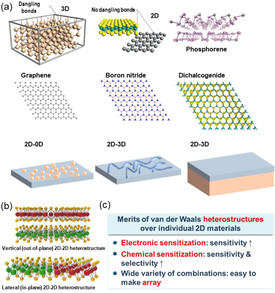
Figure 26. (a) Various van der Waals heterostructures based on 2D materials. Reproduced fromy [225]. CC BY 4.0. (b) Vertical and lateral 2D–2D heterostructures. (c) Merit of van der Waals heterostructures over individual 2D materials for gas sensors applications.
Download figure:
Standard image High-resolution imageIn 2D–0D heterostructures, 0D nanostructures such as noble metal NPs can act as effective receptors for gas molecules. Diverse 1D semiconductor nanostructures of high crystallinity such as NWs, NRs, and nanoribbons with extraordinary optoelectronic properties can become unique templates for 2D materials to achieve synergetic effects in gas sensing. Tremendous efforts have been conducted to 2D–2D van der Waals integration of different 2D materials by vertical stacking. On the contrary, lateral 2D–2D heterostructures can be achieved by controlled sequential growth (figure 26(b)). In the lateral 2D–2D heterostructures, heterointerfaces that are chemically more active than the basal plane for the adsorption of gas molecules can improve gas sensing properties. Combination of bulk 3D materials of well-defined quality and proven properties with 2D materials can bring novel functionalities which have not been exploited in either individual 2D or 3D materials. Overall, the use of van der Waals heterostructures based on 2D materials for gas sensors could bring out following merits over individual 2D materials: higher sensitivity due to ES, higher sensitivity and selectivity due to CS, and wide variety of combinations which make it possible to achieve sensor array (figure 26(c)).
22.2. Current and future challenges
There are many 2D materials commercially available. In principle, nanosheets of every 2D van der Waals material could be produced from its single crystal via liquid exfoliation. Exfoliated nanosheets are usually suspended in solution for a long time. Therefore, they are quite ready to be combined to other nanoscale materials. Since they are atomically thin, they can be integrated with other nanoscale materials regardless of lattice matching and processing compatibility. It should be noted that the van der Waals forces for each 2D nanosheet is relatively strong enough to adhere the 2D material on the nanoscale counterpart.
Graphene, a representative of 2D materials, is hydrophobic. High-yield production of graphene nanosheets is usually obtained using the Hummers method in which GO with oxygen functional groups is achieved. Hydrophilic GO nanosheets can be well dispersed in aqueous media. Facile spin coating of GO solution on a flat substrate leads to uniform coating of atomically GO thin films. rGO, which is quite conducting than insulating GO, can be obtained by thermal or chemical reduction of GO. Noble-metal-decorated rGO is promising for gas sensors. Pd- or Pt-decorated rGO shows readily sensitive and selective hydrogen sensing behaviour at RM [226]. rGO is too conducting to have large modulation in resistance upon exposure to a target gas. When rGO nanosheets have been combined with semiconducting MoS2 nanosheets that show very high resistance at RM, the resistances of rGO–MoS2 composites (RGMSs) become appropriate for chemoresistive gas sensing. As shown in figure 27(a), RGMSs exhibited much higher responses than pristine rGO and MoS2 samples [227]. The baseline resistance of the pristine rGO was 52.2 Ω, while that of the MoS2 was as high as 3.1 × 10⁸ Ω. The baseline resistance of the composites increases with the composition of MoS2. The responses of the pristine rGO and MoS2 to 50% humidity at RM were 4.1 and 70.7%, respectively. The response of the RGMS 5 composite was 872.7%, which is 220 times higher than that of pristine rGO. The drastic enhancement in humidity sensing is attributed to 2D–2D p–n heterojunctions formed between rGO and MoS2 nanosheets, an extreme exploitation of ES. The formation of van der Waals p–n heterojunctions has been confirmed by x-ray photoemission and Raman spectroscopy.

Figure 27. (a) Response curves of rGO, MoS2 and RGMS to 50% RH. Reproduced from [227] with permission of The Royal Society of Chemistry. (b) Response curves of SnS2 films on SiO2 nanorods and flat SiO2 substrate to 10 ppm NO2. Reprinted with permission from [229]. Copyright (2019) American Chemical Society. (c) and (d) Comparison of the response ratio between (c) pristine graphene and Au-decorated graphene under the self-activation state and (d) pristine SnO2 and Au-decorated SnO2 at 300 °C. Insets exhibit the sensing response of the sensors to different gases. (c) and (d) Reproduced from [230] with permission of The Royal Society of Chemistry.
Download figure:
Standard image High-resolution imageSemiconducting 2D transition metal disulfides are promising for chemoresistive sensors. In nanosheets of transition metal disulfides, the edges are active sites for the adsorption of gas molecules, while the basal planes are quite inert [228]. Transition metal disulfides such as MoS2 and SnS2 films on 1D SiO2 nanorod templates showed much higher responses to NO2 than those on flat substrates. The response of 70% to 10 ppm of NO2 with a theoretical detection limit of 408.9 ppb and excellent recovery at RM was achieved from uniformly distributed SnS2 on SiO2 NRs, which is 5.5 times higher than SnS2 film on flat SiO2 (figure 27(b)) [229]. SnS2 nanograins on the 1D template exhibited p-type conduction behaviour probably due to excessive sulphur component (Sn:S = 1:2.33) originating from numerous S-termination of SnS2 nanograins. The studies provide a new perspective of 2D–1D van der Waals heterostructures for gas sensor applications.
2D–0D van der Waals heterostructures can show unique sensing properties which have never been observed in conventional MOS. An unexpected substantial enhancement in H2 detection has been found in graphene with Au nanocluster decoration [230]. To demonstrate whether enhancement on H2 sensing properties by the 1D Au nanoclusters are unique on 2D graphene layers, sensing properties of SnO2, the representative metal oxide gas sensing material, thin film with and without Au nanoclusters have been studied as shown in figures 27(c) and (d). The graphene sample showed 48.8 times enhancement in H2 detection by Au decoration. In contrast, the SnO2 sample exhibited only 1.22 times enhancement by the Au decoration. DFT calculations revealed that van der Waals gap between Au nanocluster and graphene is responsible for the adsorption of H atoms that does happen on the surfaces of Au and graphene. The unique sensing properties of Au nanoclusters/graphene 2D–0D heterostructures suggest that further researches in the existing material platform related to noble metal/2D heterostructures have great potential for finding new functionalities holds the key exotic results for gas sensing.
One of big challenges of van der Waals heterostructures for gas sensors is detection of VOCs. A number of studies have been reported for NO2, NH3, and H2 detection with 2D materials, but reports on VOC detection with 2D materials are rare. In conventional MOS, the detection of VOC gases such as acetone, toluene and benzene usually need high operating temperatures (>250 °C) that are provided by micropatterned Joule heaters. Most of 2D materials are not stable at the high temperatures due to oxidation. To detect VOCs at lower temperatures than 250 °C, incorporating catalysts that have good activities to facilitate the adsorption and decomposition of VOC gases at the surface of the sensor material in a process referred to as the spillover effect. Noble metals and p-type transition MOS such as Co3O4 are candidate catalysts. Cross sensitivity with NO2 and NH3 should be checked simultaneously. The other big challenge would be long-term stability. The basal planes of nanosheets or nanoflakes of 2D materials are quite stable against unforced chemical reaction. However, the edges are vulnerable to chemical reaction such as oxidation and hydration. Long-term stability tests of van der Waals heterostructures for gas sensors should be carried out. Then, strategies to improve the long-term stability will be presented. van der Waals heterostructures based on atomically thin 2D materials are mechanically flexible and optically transparent. Thus, high responses to certain target gases at relatively low temperatures guarantee the application to flexible transparent gas sensors. Another opportunity of van der Waals heterostructures is the combination with micro-LEDs. UV and visible light can activate van der Waals heterostructures for improving gas sensing properties. Ultrafast carrier transport and large photoresponsivity in van der Waals heterostructures may lead to high performance gas sensing. Using micro-LEDs, low-power-consumption (submilliwatts level) gas sensors based on van der Waals heterostructures can be demonstrated.
22.3. Concluding remarks
van der Waals heterostructures including 2D–2D, 2D–0D, 2D–1D, and 2D–3D heterostructures have merits over individual 2D materials for gas sensing in terms of sensitivity and selectivity. There are thousands of possible combinations of van der Waals heterostructures which make it easy to fabricate sensor array for electronic nose [231]. First-principles calculations to understand the details of the specific properties of van der Waals heterostructures and the electrochemical interactions with analytes would boost further researches on gas sensor applications [232]. van der Waals heterostructures gas sensors of high sensitivity, good selectivity, fast response and recovery, low power consumption and outstanding stability have great promise for the use in the IoT era.
Acknowledgments
The author thanks Dr Seokhoon Choi for help me to prepare a figure. This work was financially supported by the Future Material Discovery Programme (2016M3D1A1027666, 2018M3D1A1058793) the Ministry of Science, ICT & Future Planning (2019M3E6A1103818), and the Nano·Material Technology Development Programme (2016M3A7B4910) through the National Research Foundation of Korea.
23. Platinum functionalization of chemical sensors
Marcelo Ornaghi Orlandi
São Paulo State University (UNESP), Brazil
23.1. Status
It is well known that metal oxide semiconductors (MOS) are excellent materials for gas sensing applications. As a rule of thumb, n-type MOs are used to detect oxidizing gases while p-type semiconductors are mostly used for reducing gases. However, the material selectivity can be altered by the use of noble metal nanoparticles (NPs) on the surface of the semiconductor. This process can be done by surface decoration, assuming no (or small) diffusion of the noble metal to the matrix, or by doping, when the noble metal migrates to the semiconductor crystalline structure. It is worth to mention that the best process depends on the desired application of the sensor.
The process of surface functionalization can modify and/or improve the sensor in two different ways: electronic sensitization (ES) or chemical sensitization (CS) [233, 234]. In the ES there is a charge transfer from the metal oxide (MO) to the NP, creating a depletion layer adjacent to the interface MO–NP. This depletion layer alters the MO conductivity and it is dependent on the interaction of the NP with the gases present in the atmosphere. On the CS process, the noble metal NP act as a catalyst (preferential site) to accelerate a desired chemical reaction with the target gas, which then will react with ions at the MO surface (usually ionosorbed oxygen) [234]. In fact, both are present in most of cases, but usually there is a dominance of one process in the sensor response.
The functionalization process can be made by chemical routes, for instance sol–gel, or physical ones, such as sputtering. ALD method [235] is also gaining attention on the literature due to the controlled deposition of a thin layer on the material surface. Although ALD can be a good route from the scientific point of view, just sophisticated sensors could use this process due to its higher cost.
Several noble metal NPs have been tested as catalyst on the MOs, and platinum (Pt) has attracted intense attention due to its potential to act in either electronic [236] or chemical [237] sensitization. Assuming a parabolic band potential for the outmost electrons in the platinum, the theoretical charge carrier density is 6.5 × 1028 m−3, resulting in a work function of 5.9 eV. This is close to the experimental 5.7 eV value reported in the literature [238]. Moreover, taking into account that NPs decorating the MO surface are usually in oxidized state, and the reported Pt/Pt2+ reduction potential ∼1.2 eV, the oxidized NPs are strong acceptor of electrons from the MO material, and a depletion of electrons is created at the metal oxide interface. Platinum can also produce strong catalytic effects, especially for H2 analyte at elevated temperatures, first promoting the molecule dissociation, and then allowing hydrogen to spill over the MO surface to react with ionosorbed oxygens. It means that surface decoration/functionalization can change the selectivity of sensors [239], which is important when thinking about the construction of devices based on sensor arrays for multiple gases detection.
23.2. Current and future challenges
The field of chemical sensors has continuously grown in the last decades and it is gaining more attention from researchers and publishers, which launched several dedicated journals to this field. It means that huge advances are still expected on sensors.
One important contribution to the sensors field is coming from the theoretical predictions. Nowadays, software calculations based on the DFT, like Vienna Ab initio Simulation Package [240] are more accurate in predicting materials properties due to corrections introduced in the lasted versions. This means that scientists and companies will be able to take advantage of these tools to develop a better performance sensor. In practical terms, it will be possible to predict which materials are more susceptible to have change in the charge carrier density if a Pt cluster is added at its surface. It is important to mention that there is no 'general' good sensor. A sensor device will be good if it works for the specific application it was developed.
Moreover, if well known that the amount of published papers per day is impossible to be followed by researchers. However, computers can easily storage the available papers in the literature, creating a huge data centre of knowledge. The use of Big Data and machine learning algorithms can support researchers by classifying the available papers about the effects of Pt functionalization on different materials. It will provide us a better idea about ways to follow in order to get a desired sensor response and selectivity. Nevertheless, the word 'materials' is a wide term, and the same material composition with different morphology and/or crystalline structure can provide different sensor responses when exposed to the same target gas. Then, although the machines can (and will) be extremely helpful, there is no substitute for a human being about taking the final decisions.
From the experimental point of view, the use of controlled layers of Pt over different materials by AL deposition will still provide us additional knowledge about this noble metal action mechanism. In addition, the use of advanced experimental techniques, such as XAS, DRIFTS, in situ TEM, can also be used to elucidate with more accuracy the sensing mechanisms acting in each case [241]. Finally, composites can also be decorated/functionalized by Pt NPs, and the correct choice of materials will determine which one will be used in the next generation sensor devices.
23.3. Concluding remarks
In the last years we have seen an increased number of scientific works using Pt NPs to decorate the metal oxide surfaces aiming to improve or change the material selectivity to a specific gas, most usually hydrogen and CO. This is still an open field of research and the use of computational calculations to determine the effects of surface functionalization on different materials can help researchers to save time, money and energy.
Acknowledgments
The author acknowledge the São Paulo Research Foundation (FAPESP) (#2017/26219-0), the National Council for Scientific and Technological Development (CNPq) for general research funding (#305437/2018-6) and the Coordenação de Aperfeiçoamento de Pessoal de Nível Superior (CAPES) (#88887.469365/2019-00).
24. Pd-based sensing materials for gas sensors
Ali Mirzaei1, Hyoun Woo Kim2, Sang Sub Kim3
1Yasuj University of Medical Sciences, Iran
2Hanyang University, Republic of Korea
3Inha University, Republic of Korea
24.1. Status
Resistive-based gas sensors, commercialized about 60 years ago by Taguchi, work on the basis of resistance changes that occur upon exposure to gases [104]. Different types of materials such as MOs, graphene, CNTs, MOFs and conducting polymers have been used for the realization of resistive-based gas sensors. Among them, semiconducting metal oxide-based gas sensors are the most popular due to their particular features such as high responsiveness, high stability, short response/recovery time, simple operation, small size and low cost. However, they have poor selectivity and require high temperatures to exhibit their best sensing performance [242]. In addition, their responses to target gases should be further improved to meet the high standards of today. To deal with such shortcomings, different strategies have been used over the past years such as composite making, increase of surface area, doping and noble metal functionalization. Noble metal functionalization has proven to be a simple and highly popular technique in which different noble metals including Pt, Pd, Au and Ag are extensively used for the functionalization of MOS. Pd in particular has captured great attention due to good catalytic activity and unique electrical properties. Different techniques such as chemical reduction, electrochemical reduction, evaporation, UV-irradiation, sputtering, and so on, can be used for dispersion of Pd NPs on the surface of sensing layer [243]. Generally a post heat-treatment is necessary to enhance crystallinity and dispersion of Pd over the sensing layer [33].
Enhanced gas response in the presence of Pd can be attributed to electronic and CS. In the former case, when exposed to air, Pd can form PdO that acts as a strong acceptor of electrons. Thus, in the sensing material near the interface, it induces a surface layer strongly depleted of electrons. Upon exposure to a reducing gas, PdO is reduced to metallic Pd and it relaxes the electron depletion layer by giving electrons back to the sensing layer, leading to a large increase in response to the gas. Such a change in the oxidation state of the Pd will induce a sensor signal. CS, on the other hand, is related to the catalytic activity of Pd. In fact, gas molecules such as oxygen can be easily decomposed on the surface of Pd, and in a so-called spillover effect move to the neighbouring metal oxide. As a result, more oxygen can be adsorbed on the surface of sensing layer in a shorter time. Hydrogen molecules are also susceptible to dissociation on the Pd surface and hydrogen migrates to the surface of metal oxide. Thus, Pd significantly enhances the reaction of the gas on the sensing layer. Both sensitization mechanisms in Pd decorated gas sensors can result in a gas sensor with high sensitivity, selectivity, short response time and low sensing temperature. Accordingly, there are many reports about enhanced-gas sensing properties by Pd-functionalization [244–246].
Furthermore, since the work function of Pd is generally higher than that of sensing layer, Schottcky junctions form at the contact interfaces between Pd and sensing material. When the sensor is in target gas atmosphere, due to interaction of gas with adsorbed oxygen ions on the surface of sensor, electrons will be liberated and come back to the surface of sensor, leading to significant reduction of Schottcky barrier height and modulation of sensor resistance [232, 247].
Pd can be used not only for functionalization of resistive-based gas sensors, but also for detection of H2 gas. In fact, Pd has high capacity for adsorption of hydrogen gas, so can be used for sensing of hydrogen. Two sensing mechanisms for metallic Pd gas sensors have been reported for hydrogen detection. In the first mechanism, H atoms adsorbed on the Pd act as electron scattering centres that eventually lead to change in the resistance of Pd. In the second mechanism, structural changes occur upon adoption of hydrogen into Pd lattice resulting in formation of PdHx . As a result of this conversion, the lattice constant of Pd increases up to 3.6%. Thus, an overall expansion of Pd occurs, which is so-called H2-induced lattice expansion [233].
24.2. Current and future challenges
A major concern associated with noble metal functionalized gas sensors is poisoning by toxic gases, which reduce the efficiency of sensor. Poisoning significantly decreases the number of adsorption sites on the surface of the sensing layer. Noble metals such as Pd may be poisoned by sulfur-containing compounds such as H2S, SO2, thiols, and phosphorous. Poisoning can be avoided or decreased by using appropriate filters or by post treatment through annealing. Also, a core–shell structure, where core is Pd, can be a good way to reduce the poisoning of Pd. However, due to limited accessibility of Pd to air and target gas in a core–shell arrangement, sensor performance will be decreased. A good way to deal with this decreased performance is by the introduction of porosity in the shell layer [243]. Another problem associated with Pd functionalized gas sensor is sensing temperature. When the sensor works for long periods at relatively high temperatures, Pd NPs may become agglomerated and therefore suffer diminished effectiveness. To overcome to this issue, operation of the sensor in self-heating mode can be beneficial. In this case, an external voltage will be applied to the sensor at RM which can internally heat the sensor device effectively via Joule heating. Another issue is the need for optimization of Pd amount on the surface of gas sensors. If too low, there is no efficient catalytic activity and if too high, connections between Pd NPs lead to a decreased number of adsorption sites on the surface of gas sensor. Accordingly, an optimized quantity of Pd NPs is necessary to have the highest performance gas sensor.
Two further metallic Pd gas sensor problems are hysteretic resistance and structural deformation. In particular, volume expansions because of repeated exposure to hydrogen gas can significantly weaken the Pd sensor. Also, a high concentration of hydrogen can lead to severe cracking and delamination of the Pd sensor. Moreover, since the diffusion coefficient of hydrogen in Pd film is low (3.8 × 10⁻⁷ cm2 s−1) at RM, the dynamics of the sensor will be short. Therefore, instability of the Pd sensor in high concentrations of hydrogen gas is a serious problem, while at low concentrations of H2 gas (<1%), long response times limit practical applications. There are some strategies to lessen the instability of Pd resistive gas sensors. The first is expansion of the Pd lattice before exposure to hydrogen gas. Thus, the expanded lattice has larger spaces for hydrogen atoms to easily diffuse into the Pd sensor. This can be achieved through alloying Pd with other metals such as Mg. The second strategy is to use Pd NWs, which have significantly lower structural change relative to their micro-sized counterparts. However, for increased sensor dynamics the sensing temperature should be increased.
24.3. Concluding remarks
The field of chemiresistive gas sensors is rapidly growing and novel nanomaterials and nanostructures with high surface area have become gradually more available. For example, metal–organic frameworks with potential for engineered pore sizes provide a good platform for dispersion of Pd NPs on their surfaces. Therefore, a combination of Pd with hybrid nanocomposites such as MOS/MOFs may result in fabrication of highly sensitive and selective gas sensors.
Acknowledgments
This research was supported by Inha University.
25. Ag-based sensing materials for gas sensors
A S M Iftekhar Uddin
Metropolitan University, Bangladesh
25.1. Status
With the continued expansion of industries and technological advancements, the development of gas sensors for the detection of toxic, flammable, and corrosive gases has become increasingly important for environmental monitoring, personal safety protection, and smooth industrial functionalization. In recent years, in addition to the traditional solid-state gas sensor properties, these applications require a number of additional features such as cost-effective device fabrication, lighter weight, flexibility, and stretchability to enable smart wearable, handheld and portable gas sensors. For this, flexible gas sensors have attracted considerable attention due to their low cost, mechanical stability, and biocompatibility, making them promising candidates for various applications, such as aeronautic transportation, portable electronics and small textiles, or radio frequency identification. However, the expected performance of these sensors has not yet been realized adequately in practice due to the requirement of operating temperature, continuous monitoring, replacement of batteries, durability, and environmental effects. Moreover, under the context of the current technology, most of these flexible gas sensors need power sources for driving their operations, which is a major limitation for realizing the wearability and portability features for practical applications.
Therefore, realizing self-powered operation for the sensor nodes in the sensor networks is critically important for the broad applications of such networks, which is gradually becoming a major research direction in this area. The most feasible way to achieve self-powered operation is to harvest energy from ambient environment to drive a sensor node itself. The realization of self-powered active sensors generally has two approaches: the first approach is to develop environmental energy harvesting devices for driving the traditional sensors; the other is to develop a new category of sensors self-powered active sensors that can actively generate electrical signal itself as a response to stimulation/triggering from the ambient environment. More elaborately, the energy harvesting device can directly serve as a sustainable power source for the sensor node or at least use together with a battery to replenish its energy consumption. Besides, if the sensor can generate electric signal itself as a response to the trigger or change in the environment, it can operate without an external power source, which is named as 'active sensor'. With this strategy, the sensor system can be simplified, and the total energy consumption can be largely reduced. Thus, developing self-powered active sensors can largely facilitate the wide range of practical applications for sensor networks.
Most recently, harvesting green energy using a triboelectric nanogenerator (TENG) that employs triboelectrification has attracted great interest due to its simple and cost-effective fabrication process, miniature size, light weight, easy scalability, outstanding flexibility, diverse formats of mechanical triggering, and biocompatibility. To realize the TENG-based sensor, the bulk TENG systems are generally altered with specific sensing materials that are chosen according to the catalytic property related to the target gas species. To date, a number of TENG based self-powered active sensors have been reported with possible advancements [248–251]. A brief description of the reported works is depicted in figure 28.
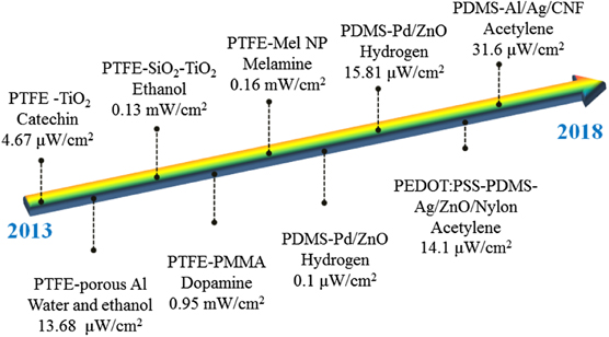
Figure 28. Research trend of TENG based chemical gas sensor.
Download figure:
Standard image High-resolution imageIt has been revealed that surface modified polymer surfaces, combination of proper contact materials, coating of appropriate sensing materials (specific to gas molecule detection), and suitable device structures are vital for the development of self-powered active sensors. Moreover, addition of intermediate layer and stacking of layers can preferentially enhance the TENG sensors under specific environmental impacts. However, in every case, emerging of specific sensing materials with one friction layer significantly degraded the output of the nanogenerator itself. In order to overcome these limitations, such a TENG based sensor should be considered that will be capable of generating high output voltage as well as enhanced sensing properties without the need of replacing any friction layer with sensing-friction layer. Among of various metals (such as aluminium, copper, gold, etc) that have been widely used as positive friction materials in TENG sensor, silver (Ag) nanostructures can be the best option as it has high tendency to be positive during triboelectrification as well as better catalytic property towards hydrocarbons.
25.2. Current and future challenges
From the literature it is evident that in acetylene (C2H2) sensing (chemiresistive-type), Ag plays an important role in enhancing the sensing performance [252, 253]. Due to the catalytic property of Ag, spill over zone is formed in any Ag-composites and/or Ag-hybrids, which creates additional active sites and help to adsorb required number of C2H2 molecules on the sensing surface. However, pristine Ag or dominating Ag in TENG sensor show the inferior sensing impact than Ag-composites or Ag-hybrids based chemiresistive sensor. Importantly, the relatively slow response–recovery time characteristics, requirement of high external contact force and/or frequency, random input from the energy harvesting sources to the TENG sensor are still the subjects of intensive research. On the other hand, humidity has negative impacts on the triboelectric response, which is also a major concern in the development of TENG sensors.
According to Uddin et al, bimetallic Al/Ag semi-continuous film can provide direct friction with the opposite friction layer to maintain the TENG performance and show better sensing performance towards C2H2 gas molecules as well. In addition, the outstanding mechanical flexibility and stability of the Al/Ag network and the improved surface roughness of the friction layer can decrease the influence of humidity on device performance. From the literature, it is expecting that the consideration of Ag nanostructures with improved surface roughness, adequate pores on the Ag surface for gas molecule injection, convenient design mechanism and structure with the workability under a broad variety of external impacts from the environment will be helpful to overcome the current challenges and will ultimately boost the development of high performance TENG sensor for practical sectors.
25.3. Concluding remarks
Though response–recovery time characteristics, influence of humidity and stability of the TENG-based self-powered sensors are comparatively inferior than the sensors prepared by other mechanisms such as chemiresistive, electrochemical, surface acoustic, etc, the performance of the TENG-based self-powered sensors can be tuned by enhancing the triboelectric charge density on the contact materials, selecting suitable mechanism, considering the wide-ranging external impact competent device structure and possible material nanostructures (from the tribo-series materials). It is expecting that the current challenges can be overcome by adopting sensing layers' setup sequence from bottom approach to top approach and will provide a new avenue of research for the development of high-performance sensors for practical applications.
26. Au-based gas sensing materials
Jing Wang1 and Yi Xia2
1Jiangnan University, People's Republic of China
2Kunming University of Science and Technology, People's Republic of China
26.1. Status
Although elemental Au itself does not act as a gas sensing material, one should note that a large number of semiconductor gas sensors, i.e. chemiresistors, are fabricated based on nanocomposites composed of the metal oxide film or nanostructures functionalized by Au NPs. The incorporation of Au into metal oxide gas sensors for promoting the surface catalytic reactions can date back to several decades ago. Till now, a variety of methods, including thermal evaporation, sputtering, impregnation, sol–gel, solvothermal reduction, colloidal assembly and photochemical deposition have been used for introducing Au NPs or nanoclusters onto metal oxide surfaces, and these different methods may lead to different Au state, particle surface and interfacial properties [254, 255]. By using Au NPs functionalization, the gas sensing properties of MOS can be improved in many aspects including reduced operation temperature, increased response, improved selectivity as well as decrease response and recovery times [33]. In addition, the optical absorption properties of Au nanoparticle also renders the possible application towards optoelectronic gas sensors.
Commonly, two concepts are invoked to explain the effects of Au functionalization on metal oxide's sensing performance (figure 29) [62, 256]. One is the 'ES' proposal and the other is a 'CS' process. In ES, the work function of Au is always higher than that of the metal oxide semiconductors, so when Au NPs are decorated onto metal oxide surface, electrons are expected to flow from MOS to Au NPs across the interface until the Fermi level is equalized between the two materials, leading to the formation of a depletion region near the metal oxide surface. As a result, the band of metal oxide bends and forms a 'Schottky junction' at the interface, hence the width of the conduction channel in metal oxide can be modulated. The increased resistance modulation from electron depletion in the metal oxide material and increased surface activity in the heterostructure may boost both sensitivity and selectivity. However, the 'ES' concept cannot well explain the temperature dependent gas sensing behaviour of Au-functionalized MOS, thus one should also consider the 'CS' concept. In CS, the gas molecules can absorb onto the Au nanoparticle surface with reduced adsorption–activation energy, and then dissociates into chemisorbed atomic species, which can efficiently trigger the surface reactions between analytes and oxygen. Moreover, the accumulation of electrons in the Au nanoparticle caused by 'ES' can further promote the adsorption of electronegative species such as oxygen. Therefore, the above two concepts are closely linked, and they may both happen simultaneously in most composite sensing materials.
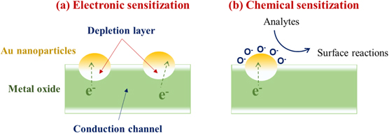
Figure 29. Schematic illustration of ES (a) and (b) CS of Au metal promoter on metal oxide surface.
Download figure:
Standard image High-resolution image26.2. Current and future challenges
In recent years, the application of Au nanoparticle functionalization has been extended from MOS to other functional sensing materials including other semiconductors such as TMDC, conducting polymers, and some carbon-based nanomaterials such as CNTs and graphene [257]. Enhanced gas sensing performances of these nanocomposites can be achieved by designing the backbone semiconductor materials based on the two sensitization effects. Since the ES effect is closely related to the morphology feature and electronic properties of the semiconductors, intensive efforts have been devoted to the fabrication of the semiconductor materials with controlled size and dimension. 1D and 2D NSs are considered as most promising candidates for construction of the Au-containing nanocomposites, since their excellent carrier transport ability and confined dimension will maximize the ES effect of Au NPs. Construction of ternary hybrids composed of semiconductor, Au NPs and nanocarbons is also studied, considering the advantage of the excellent charge transport capacity of nanocarbons. For future research, we suggest that some new materials such as perovskite, metal–organic frameworks and MXenes can be combined with Au NPs and explored for gas sensing applications.
Since the CS effect rely on the catalytic activity of the Au NPs, the well-established strategies in the Au catalyst research can be employed in gas sensing applications. Therefore, the controlled synthesis of Au NPs with different morphology, composition, size, facet and surface properties should lead to varying sensitization effect on semiconductor sensing materials. For example, the different exposed facet may affect the adsorption and activation energy of analytes, thus faceted Au NPs can be designed to adjust the selectivity to a certain analyte. In addition, enhanced gas sensitivity of Au NPs may be also achieved by tuning the size and surface properties of Au NPs to improve the oxygen adsorption and dissociation process. The effect of co-decoration of two kinds of noble metal NPs, or Au-based bimetallic nanoparticle has been also investigated. For example, WO3 co-functionalized with Au and Pd NPs exhibited enhanced sensing performance to acetone, which was attributed to the possible formation of Au–Pd alloy [258]. For future research, we suggest that more work can be carried out on Au-based alloy nanoparticle or even some bimetallic NPs with a specific structure such as core–shell structure. Such alloy NPs with altered electronic structure, modified interfacial and surface properties are highly expected to exhibit enhanced CS effect in gas sensing.
To enhance the CS effect of Au NPs, one should also pay attention to the support effect which describes the interaction between the semiconductor materials and Au NPs, since these interactions can affect the electron transfer, heterointerfacial reactivity as well as the dispersion states of Au NPs. For example, it was revealed that the surface lattice oxygen of FeOx near Au NPs was involved in the oxidation of CO, suggesting that the Fe–O bond was activated by electron transfer from FeOx to Au NPs [259]. Therefore, the enhanced gas sensing performance of heterostructure should be also attributed to the heterointerfacial reactivity. For future research, we suggest that the semiconductor–Au interaction and synergistic effects should be more deeply investigated. For example, the interfacial reactivity may be improved by deposition of Au NPs onto the specific facet of semiconductors. Moreover, the interaction between the Au NPs and the defects (especially Ov) on MOS may also contributed to the synergistic enhancement effects.
Recent, light activated room-temperature-operated gas sensors became a research hot topic. The Au NPs can play multifunctional roles in the light activated semiconductor sensors. Under UV illumination, the wide-band-gap semiconductor can be activated and inject its electrons into Au NPs, leading to enhanced charge separation of semiconductor; under visible-light illumination, the Au NPs can be excited due to the localized SPR effect, and inject their SPR hot electrons into semiconductors, leading to the enriched free carriers in semiconductors. These different behaviour of Au NPs in dark, under UV and visible light should result in their different ES behaviour. For example, our recent work reported the different selectivity to oxidizing and reducing gases of Au NPs functionalized ZnO NRs, which was attributed to the different direction of the electron transfer [260]. In addition, some recent studies suggested that photocatalytic reactions occurred on the semiconductor surfaces during the sensing process. Therefore, the role of Au nanoparticle can be also considered as a cocatalyst for the photocatalytic reaction. In fact, the improved charge separation of the nanocomposite, and enriched photo-induced carriers on both semiconductors and Au nanoparticle should contributed to the enhanced photocatalytic performance of the nanocomposite. Considering the oxygen activation property of Au NPs, these light-activated gas sensors should be more suitable for reducing gases. For future research, we suggest that to combine the light-activated gas sensing with the photocatalysis principles to realize a higher sensing performances [261].
Last but not least, the mechanistic investigation of critical role of Au NPs in gas sensing is still of great important for maximizing the synergistic effect of the electronic and CS. Many studies reported the systematic evaluation of the Au-based sensing materials with controlled synthesis parameters, providing insight into the structure–properties relationship. However, we still need to gather information about the intermediate species and reactions occurred on the material surface, to form a fundamental understanding of the relationships between surface reactions and sensing performance. In recent years, in situ spectroscopic tools have been developed to real-time track the reaction processes on a working sensing materials under operating conditions [262]. For Au-based sensing materials, we specially suggest the employment of in situ diffuse reflectance infrared Fourier transform spectroscopy, in situ electron paramagnetic resonance, in situ x-ray absorption spectroscopy to study the chemical reactivity of the heterostructure.
26.3. Concluding remarks
Significant progress has been made on Au-based gas sensing materials in recent years, especially heterostructures composed of Au NPs and semiconductor nanostructures. The sensor performances have been largely improved by controlled fabrication of the nanocomposites with desired composition, morphology, size, surface and electronic properties. Synergistic effects of electronic and CS have been credited for these performance improvements. Nevertheless, more mechanistic investigation of critical role of Au NPs in gas sensing should be carried out for maximizing the synergistic effect of the electronic and CS.
Acknowledgments
This work was supported by National Natural Science Foundation of China (No. 51802123), the Natural Science Foundation of Jiangsu Province (No. BK20180630) and Scientific Research Fund of Yunnan Education Department (2019J0034).
27. Graphene-based gas sensors
Chatchawal Wongchoosuk
Kasetsart University, Thailand
27.1. Status
Since the discovery of the first 2D crystal graphene by Geim and Novoselov in 2004 [263], graphene has become the highlight of the researches around the world in various fields and referred as the miracle material of the 21st century. Owing to its extraordinary properties [264] such as high electron mobility at RM (∼2.5 × 105 cm2 V−1 s−1), high thermal conductivity (>3000 W m K−1), high Young's modulus (∼1 TPa), excellent strength (∼130 GPa), high electrical conductivity (∼5600 S m−1) and large specific surface area (2630 m2 g−1), graphene can be widely used in many applications and enable several disruptive technologies including electronic devices, spintronics, photonics, sensors, flexible electronics, energy storage, composites, and biomedical applications [265]. For gas-sensing applications, graphene and its derivatives have recently attracted much interest for efficient detection of several gases and VOCs with the benefits of RM operation and high signal to noise ratio [266].
27.2. Current and future challenges
Based on Scopus database, number of publications on graphene-based gas sensors increases significantly every year as shown in figure 30. Total publications from 2007 to 2019 are 1227 papers searched by using keywords of 'graphene' and 'gas sensor' on February 27, 2020. It includes 1011 articles and 216 conference papers in which China is the most contribution in the field of graphene-based gas sensing application. Among these publications, NO2 and NH3 were found to be the most popular target gases. The graphene gas sensor was first demonstrated in 2007 using the mechanical exfoliated graphene [157]. After the success of the pioneering work, several research groups tended to investigate the sensing properties of pristine graphene both experimentally and theoretically.
Figure 30. Number of publications on graphene-based gas sensors and the countries of the authors' address in their publications (inset) searched from Scopus database on February 27, 2020 using keywords of 'graphene' and 'gas sensor'.
Download figure:
Standard image High-resolution imageThe current working principles of graphene-based gas sensors can be mainly classified into chemiresistor, field effect transistor (FET), optical gas sensors and quartz crystal microbalance (QCM) [267]. The chemiresistor relies on the changing of graphene resistance upon the nature of adsorbed gas molecules. The FET uses the changing of the drain–source current induced by the adsorbed gas molecules with modulation of an applied voltage at the gate of FET. The optical type is based on the changing of optical characteristics such as absorption, transmittance, polarization, photoluminescence, colour etc as a function of gas type and concentration while QCM relates to the changing of resonant frequency due to the different molecular weight of the adsorbed gas molecules. Among them, the chemiresistor is the most widely used type of graphene-based gas sensors because of direct measurements, simple structure and fabrication, low cost and ease to use in practical applications. However, up to now, no graphene-based gas sensor is available in market yet. Most of researches on sensing properties of graphene gas sensor are in lab scale. The long recovery time, low selectivity and sensitivity of pristine graphene are still challenge in industrial level. To overcome these obstacles, four directions of graphene-based gas sensor development are proposed as follows:
- (a)Other forms of graphene such as 0D graphene quantum dots, 1D graphene nanoribbons, 2D bilayer graphene (BGR) and 3D pillared graphene. Typical 2D graphene can be cut into smaller pieces or reformed to larger dimension which provides higher surface area for gas adsorptions leading to improvement of the sensitivity. For example, BGR graphene gas sensor exhibited high sensitivity and selectivity to NO2 which is more than twice higher than that of monolayer graphene [268]. The monolayer graphene owns the unique massless conical band electronic structure that may be quite limited in the amount of charge transfer to the adsorbed gas molecules compared with typical parabolic bands of BGR. The BGR provided more charge transfer and accessible active surface area causing larger resistance change and sensitivity enhancement.
- (b)Functionalization of graphene with functional groups, i.e., GO was chemically functionalized by hydroquinone molecules in one-step hydrothermal synthesis process. The functionalized GO sensor displayed twofold higher responses to CO2 as well as faster recovery time compared to original one [269]. The hydroxyl functional groups contributed from hydroquinone molecules play an important role in improvement of NO2 sensing. They help to increase the interactions between NO2 molecules and sensing film via hydrogen bonding as well as active sites for the NO2 adsorption.
- (c)Metal/metal oxide decorated graphene. Graphene can be doped with several metal oxide or noble metals NPs such as CuO, ZnO, Sn2O, Fe2O3, TiO2, WO3, CeO2, Ag, Au etc to improve selectivity, sensitivity, response time, recovery time, and stability at RM. Decoration of metal oxide NPs on graphene can form Schottky metal–semiconductor junctions, p–p homojunctions or p–n heterojunctions leading to enhancement in sensing performances. For example, Sn–TiO2 NPs were doped in graphene/carbon nanotube (rGO/CNT) nanocomposite via the solvothermal method [270]. The Sn–TiO2@rGO/CNT gas sensor exhibited high sensitivity and ultrahigh selectivity towards NH3 against various gases and VOCs including toluene, dimethylformamide, acetone, formaldehyde, ethanol, methanol, IPA, CO2, H2, C2H2, and paint thinners due to formation of p–n heterojunctions of p-type rGO/CNT and n-type Sn–TiO2 via the low-temperature oxidizing reaction process.
- (d)Polymer–graphene hybrid systems. Graphene was usually modified with conducting polymers such as PANI, polythiophene (PT), polypyrrole (PPy), poly(3,4-ethylenedioxythiophene):poly(styrenesulfonate) (PEDOT:PSS) and so on. For example, printed graphene–PEDOT:PSS gas sensor was found to be high response and selectivity to 25–1000 ppm NH3 at RM because of due possibly to the increase of the specific surface area and interactions between the sensing film and NH3 molecules via π electrons network [271]. The main advantage of this polymer/graphene nanocomposites strategy is to enable the flexible properties that can be useful for wearable and stretchable gas sensor device.
27.3. Concluding remarks
The field of graphene-based gas sensor is still very interesting, especially MOS decorated graphene. Based on the current publications, the metal oxide decorated graphene gas sensors clearly showed high performances of sensing properties such as high selectivity and sensitivity, fast response and recovery times, good stability and humidity independent. However, the major challenges are large-scale production of metal oxide decorated graphene and manipulation of the sensing materials on electrodes with high uniform and purity. If these problems can be solved, the first graphene-based gas sensor may be available in market soon.
Acknowledgments
This work was supported by Kasetsart University Research and Development Institute (KURDI) under the Grant Number FF(KU) 25.64.
28. Carbon nanotubes for gas sensors
Anindya Nag1 and Subhas Mukhopadhyay2
1Dongguan University of Technology, People's Republic of China
2Macquarie University, Australia
28.1. Status
With the exponential use of nanomaterials for industrial purposes in the late 90s, the booming influence of CNTs took place in this area as potent NPs. Along the nature of CNTs vary based on their structure and dimensions, some of their attributes like high electrical and thermal conductivity, resistance towards the change in response with temperature and high interfacial bonding which makes them popular for forming nanocomposite-based sensors for sensing purposes, makes them one of the high recommended industrial components. Among the different sectors, these materials have been applied; gas sensing is one of the areas CNTs have been highly preferred due to their unique geometry, morphology and materials properties [272]. Even though gas-sensing has been done for a while now, the use of CNTs for these purposes started at the beginning of the last decade [273]. The significance in gas-sensing lies in the disastrous effects they can cause with their leakage in the normal and combustive environment, even in very low concentrations. CNTs have a high capability to measure gases in ppm and ppb levels due to their high nanotube electronic transport and high material adsorption as a result of large surface area. These CNTs have been prepared by various methods like CVD, arc discharge and laser ablation, which subsequently varies the resultant nature of the formed CNTs. The catalysts and gases used in each of these techniques vary the impurities generated in the system, along with the variation in the amount of chirality and metallic nature of the nanotubes. Another major reason for using CNTs-based prototypes for gas sensing is their easy and efficient functionalization with a range of organic and inorganic groups and ligands, in order to increase the sensitivity of the sensing surface towards the targeted gas. Figure 31 shows the schematic diagram of one such phenomenon where the multi-walled carbon nanotubes (MWCNTs) had been doped with nitrogen for the detection of hydrogen peroxide gas [274]. This kind of doping in CNTs is not only essential to lower the LOD for gas, but also decreases the response time and increases the robustness of the sensors when detecting for a prolonged period. The level of doping also varies in accordance with the type of functionalized component as well as the targeted analyte, as a result of the increased active sites. In terms of the nature of the prototypes used for sensing purposes, the variation in the type is caused by the processed materials, number of layers in the sensor and fabrication procedure. This variation is depended on the ease of fabrication and level of performance. Sensors have also been fabricated in the form of arrays, as shown in figure 32 [275]. The array consisted of selective material for detecting hydrogen peroxide gas with the presence of titanium and gold contact points. The advantage of having an array for a particular gas is related to the proper response of the prototype towards then gas when the testing was done simultaneously at different concentrations. In comparison to other carbon-based conducting materials like graphene and graphene, CNTs are much more advantages for gas sensing due to their lower cost and better ability to form interfacial bonds in the polymer matrix. Also, it is difficult to control the bad gap for materials like graphene, thus making it tough for doping purposes. This makes it very difficult for such materials to be used for gas-sensing purposes since the electrochemical activity would be very low without the presence of any functionalized group or selective material. There is a rise in the estimated use of CNTs in the commercial market for gas-sensing along with other applications, with the rise of the budget from 4.55 billion dollars in 2018 to 9.84 billion dollars in 2023.

Figure 31. Schematic diagram of the phenomenon of functionalization of MWCNTs for hydrogen peroxide detection. Reproduced from [274] with permission of The Royal Society of Chemistry.
Download figure:
Standard image High-resolution image
Figure 32. Schematic diagram of the representation of an array of SWCNTs-based sensors for the detection of hydrogen peroxide gas. Reproduced from [275] with permission of The Royal Society of Chemistry.
Download figure:
Standard image High-resolution image28.2. Current and future challenges
Although a lot of research has been done in regard to the use of CNTs-based gas sensing, some loopholes still exist that need to be filled. Firstly, a standardized technique for the fabrication of CNTs, specifically for developing gas sensors, is yet to be noted. Although certain techniques are being followed to form CNTs, the characteristics of these materials vary a lot. This makes it difficult to follow one particular technique for developing gas sensors. Researchers primarily follow techniques with lower impurities, but this does not guarantee high sensitivity and efficiency. From the working principal point of view, sensors working on a single, double or multiple layer, or with the presence of single or multiple selective sites, would respond to the same gases differently. Even though this would keep the researchers interested in optimizing the selective materials for increasing the sensitivity, this makes it difficult for the industries to a trade-off between the chosen characteristics of the gas sensors. One of the biggest issues faced ever since the beginning of the use of CNTs for sensing purposes is forming a homogenous mixture with water or water-soluble components. Even though the addition of certain surfactants does help in mixing them, this drastically affects the characteristics of the CNTs, especially during the formation of composites containing the active sites. Also, the presence of the surfactants reduces the electro-catalytic activity due to the percolation threshold achieved in the cell. The optimization is the amount of surfactants to be mixed in the CNTs-based nanocomposites is also an issue, especially when the nanocomposites consist of more than one conductive material. This creates an issue in regard to the trade-off done between the weight percentage of the different nanofillers mixed in the polymer matrix, to determine the dominating material in the composite. Eventually, the sensitivity of the sensors is affected during the profiling and experimentation done gas-sensing purposes. Secondly, most of the results showcased in the gas-sensing papers [276] contain the experiments done in the laboratory environment. This makes it difficult to predict if the sensors would provide equal performance in real-time applications. Also, the experiments were done in the laboratories mostly contains only one or two types of gases in an isolated environment. Whereas in reality, the real-time testing of the sensors would include a lot more gases. Although some of the sensors working on certain gases like methane or hydrogen have high sensitivity [277], most of the CNTs-based sensors show a variation in sensitivity when tested for multiple gases [278]. This makes it difficult for the sensors to be used for testing in a multifunctional manner. When the sensors would be used in certain industrial plants where multiple gases are tested and detected in low concentrations, each of the gases would require its own sensor, thus increasing the total cost. Also, when the sensors are being used for a prolonged period, there is a saturation in the response of the sensors, which deters their sensitivity [279]. This makes it compulsory to change the sensor frequently, depending upon their lifetime. The market of the CNTs-based sensors also lacks productivity, particularly for gas-sensing, since the sensors that have been used commercially have been primarily used for energy and defence purposes [280]. This makes it necessary for the sensors to be used in a multidisciplinary manner where the fabricated prototypes would have a compulsory detecting capability of sensing gases. These above-mentioned points need to be worked on, in addition to some of the novel attributes that can be considered for these sensors. Sensors should be developed where the operating range is very high so that a single sensor would be able to detect the low and high gas concentrations. Researchers should also consider forming prototypes with increased reusability. This needs to be done since a selective material applied through techniques like molecular imprinting technology has the capability to operate maximum for a few rounds of experimental cycles, after which they need to be changed. The fabrication of sensing areas of the prototypes consisting the selective can be done to minimize human interference during the real-time application. The involvement of other nanomaterials should be increased to operate on the cumulative attributes of the individual components. The formation of embedded sensing systems should also be encouraged where the responses collected from the detection of multiple gases can be multiplexed by the signal-conditioning circuit to send to the monitoring unit.
28.3. Concluding remarks
CNTs being highly effective due to their electrical and mechanical properties forms a cornerstone for forming gas-sensors. In addition to the amount of work on this sector, there is still a very high potential to work on CNTs-based gas sensors, considering on above-mentioned challenges and future work. Each of the steps, including the fabrication technique, functionalization and implementation of the nanotubes for gas sensing, has to be worked on to develop multifunctional CNTs-based sensors having a low cost of fabrication, high robustness, sensitivity and resilience towards the changes in the temperature and humidity of the environment. The optimization of CNTs-based sensors for gas-sensing should be continued in order to achieve highly efficient commercial sensors for domestic and industrial purposes.
29. Advancements in nanocomposites for gas sensors
Nupur Saxena and Pragati Kumar
Central University of Jammu, India
29.1. Status
Nanocomposites are advanced materials that harness the synergetic and complementary effects of its ingredient materials to eliminate the drawbacks and overcome the limitations of single materials. For illustration, high operating temperature and low selectivity of inorganic materials, and poor chemical stability and mechanical strength of organic materials restricts their practical application in gas sensing [281]. Hence, nanocomposites are broadly synthesized using organic–organic, organic–inorganic and inorganic–inorganic materials (figure 33). There is plenty of literature available on gas sensors using numerous nanocomposites and paid enormous interest due to its advanced properties and performances.
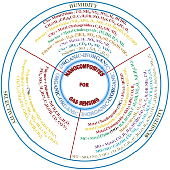
Figure 33. Status and challenges of nanocomposite-based gas sensors.
Download figure:
Standard image High-resolution imageAs far as polymer-based nanocomposites (PPNCs) are concerned, entire focus is on PANI due to its superior properties over other polymers viz; simple and reversible doping–dedoping chemistry, stable electrical conduction mechanisms, high environmental stability and ease of synthesis. Because of these excellent properties, PANI drives it towards potential electrical device applications. In addition, PANI exhibits diverse chemical structures and different response mechanisms upon exposure to different gases. PANI nanocomposites have been used for the sensing of various gases like NH3, H2, HCl, NO2, H2S, CO, CO2, SO2, and LPG etc along with vapour of VOCs and chemical warfare agents (CWAs). Highly sensitive NH3 detection at level 1 ppm, 25 ppb and 50 ppt has been carried out using PANI/PMMA by Zhang et al [282] PANI/SWCNTS by Li et al [281] and PANI/TiO2 nanocomposite by Gong et al [281] respectively, whereas high sensitivity, selectivity, and response towards 4% H2 gas diluted in air at RT is shown by Li et al [282] using chitosan/PANI and for H2S (0.1 ppb) by Shirsat et al using PANI–Au nanocomposite. Besides, explosives, and CWAs like cyanide (50 ppm), phosgene (0.1 ppm), and dimethyl-methyl-phosphonate has been detected by Hosseini et al using polystyrene-graft-PANI, Virji et al using amine–PANI nanofiber and Yoo et al using PANI–MWCNTs respectively [282].
Carbon nanostructures (CNs) (e.g., CNTs, graphene and its derivatives, carbon black, and carbon fibres) based nanocomposites have gained superfluous attraction as sensing materials and widest range of gas species have been detected using these. Qi et al demonstrated fast detection (1–2 min) of NO2 (10 ppb) using CNTs/PIE, relatively fast detection (21 s) of H2 (35%) observed by Jung et al using CNTs/Co3O4 and ultrafast detection (7 s) of NH3 (1%) by Cui et al using CNTs/Ag [60]. The dominance of CNTs and its nanocomposites in gas sensing is now challenged by graphene and its derivatives due to large specific surface area, carrier mobility and more flexibility of 2D planar surface which offers better processing to be integrated into the fabrication of electronic devices. Novoselov's group [283] has demonstrated first in 2007 that detection of individual gas molecules is possible by micrometer-size sensors made from graphene. Singh et al [284] observed detection of common industrial toxins like CO, NH3 and NO for concentrations as low as 1 ppm at RT using rGO/ZnO, whereas fast detection (6 s) of NH3 (10 000 ppm) using rGO/Ag was shown by Chen et al. Zhou et al have detected H2S (5 ppb) with fast response of <2 min and 11% sensitivity using Cu2O-functionalised graphene nanosheets and ultra-fast detection (9.6 s and 7.3 s) of NOx (97 and 100 ppm) was illustrated by Yang et al group using graphene/Cux O and graphene/CeO2 respectively [60].
MOS (MO) are the backbone for sensors not just in the category of inorganic–inorganic nanocomposites but also in organic–inorganic (figure 33). Despite the limitation of operating temperature above RT, many successful efforts have been demonstrated at RT. For examples; Pd/SnO2 has been used for the ultra-sensitive detection of H2 (10 000 and 1000 ppm) with response, response time and LOD as ∼120 000 & 12, ∼2 s & 4 s, and 40 ppm & 20 ppb by Lei et al and Wang et al respectively, whereas Ag/TiO2 and Au/ZnO were used by Zhu et al and Hosseini et al for efficient detection of C2H5OH (5 ppm) and H2S (3 ppm) with LOD 15 ppb and 50 ppb respectively. Zhou et al and Tang et al were able to detect NH3 (100 ppm and 0.4 ppm) with response & response time of 1.9 and 10 000 & 2 s and 20 s using In2O3/CuO and Fe2O3/ZnO respectively [285]. Similarly, MCs have been utilized together with other inorganic materials for advanced sensors e.g. Saxena et al [286] demonstrated LPG (1000 ppm) detection using CdS/SiO2 nanocomposites with response of ∼71% and LOD as 20 ppm.
29.2. Current and future challenges
The nanocomposites are proven an effective way to overcome the limitations of individual materials. However, certain critical issues related to nanocomposites or their constituents need special attentions. There are mainly two kinds of structures formation in case of PPNCs: blends and coaxial cables by various synthesis approaches. Usually, the coaxial cable structured composites are prepared through two-step processes and possess the difficulties particularly of proper alignment and uniform distribution of fibres. In contrast, the synthesis of 1D blend is trickier, primarily due to need of common solvents [287]. Besides, PPNCs display poor mechanical strength, complex sensing mechanism for different target species, degradation in due course of time, reproducibility, and slow response.
On the other hand, CNs nanocomposites have critical issues related to the CNs particularly that stuck their real applications. The challenges include development of low cost synthesis method of semiconducting SWCNTs or the removal of metallic SWCNTs from the SWCNT bundle, growth of defect-free nanotubes continuously to macroscopic length, precise control over uniform dispersion/distribution and alignment of CNTs, control over band gap of graphene, reproducibility and extensive processing of rGO, incomplete recovery of graphene, degradation in the sensor performance/quality (reproducibility, long-term stability, and false control etc) on large scale fabrication. In short, improvements in the production of sensors are highly needed for their commercialization and research is needed to develop cost effective and scalable production methods that can retain essential properties of CNs materials. The theoretical indulgent is needed for interaction mechanisms between various gases and CNs nanocomposites in advent of production of advanced sensors [285].
There are broadly two approaches used to synthesise polymer–inorganic nanocomposites; in situ polymerization/copolymerization and physical mixing [288]. In former case, control on concentration of inorganic material and its distribution are critical issues whereas later one is relatively time consuming process. Besides processing challenges, one limitation associated with noble metal–organic composites is their cost-effective fabrication due to pricey noble metals. In contrast, organic–MO/MC nanocomposites have serious issues of elevated operating temperature [285]. Further, challenge is to improve binding of nanocomposites with electrode/conducting platforms and the tuning of energy barrier at the interface for easy charge transport that is required for improved sensing. However various electrode treatments viz; such as hydrogen/nitrogen/plasma treatment, higher temperature annealing, self-assembled monolayer modification, etc have been introduced for efficient sensor platform development. Moreover, good analyte adsorption at the nanocomposite sensing surface and effortless carrier transport to electrode is required for gas detection at the ppt level [281]. Perhaps, organic–inorganic nanocomposites have dazzling forecast for gas monitoring, but selectivity is the key concern. Indeed, development of optimized target–analyte-specific nanocomposites is mandatory. The studies, modifications and science focussed on the interface between organic–inorganic nanocomposites along with systematic inspection of consequences of humidity are essential. CNs–inorganic nanocomposites have serious concern of insufficient sensitivity and response rate, slow recovery time at RT for practical applications besides other issues discussed above.
The key issue associated with MO–MO, MO–MC, MC–MC is poor sensitivity and slow response at RM under lower concentration along with infrequent one step and cost-effective synthesis method. Besides, MC–MC is not explored broadly and deeply. SiO2 based organic/inorganic nanocomposite sensors usually respond slowly because of its chemically and physically inert nature.
29.3. Concluding remarks
In summary numerous materials has been bring into play to fabricate organic–organic, organic–inorganic and inorganic–inorganic nanocomposites in the forms of variety of shapes, sizes, and structures and explored their sensing activities of diverse gases. These nanocomposite structures offer impressive gas sensing properties. Indeed, the huge number of efforts suggests that often the coupling of similar materials demonstrates different results. In fact, this occurs because the choice of the materials is not the only parameter to be taken into account for designing of high-quality sensor but the size, shape, and ratio of the two materials is essential along with the synthesis processes and parameters may play a key role. Besides, the surface to volume ratio, accessible fractional active surface, the chemical/physical bonding, transportation of charge carriers, and concentration stoichiometry defects or impurities at interface/surface can all contribute to the sensing mechanism and the final response of the device. In nutshell, all these factors must be taken into account to design nanocomposite sensing device with excellent features including RT operation, minimizing energy consumption and cost, high-precision with high sensitivity, fast response, good selectivity, low LOD, as well as in situ and real-time monitoring capabilities, increasing security and stability, realizing device miniaturization and suitability for handheld operations for the purpose of common use/commercialization.
Acknowledgments
NS is thankful to Council of Scientific and Industrial Research (CSIR), New Delhi, India for providing SRAship under the Scientists' Pool scheme (Pool No. 8920-A).
30. Electrochemical gas sensors based on conducting polymer composites
Jing-Shan Do
National Chin-Yi University of Technology, People's Republic of China
30.1. Status
Since 1977, the preparation, characterization and applications of electronic conducting polymers including in the fields of energy (energy reserve and solar cells), sensing materials (liquid and gas phase analysis) and environmental remediation (capture of cations and anions, degradation of harmful substances, adsorption of pollutants) have been widely studied and discussed [289]. Electronic conducting polymers also named as intrinsically conducting polymers (ICPs) have generally the conjugated double bond. The formation of delocalized π-electron accompanied with doping/undoping the counter ions result in the conduction of electron when the redox of ICPs. ICPs, including polyacetylene, poly(p-phenylene), polyfuran, PT, polycarbazole, polyimonodibenyl, PPy and PANI, and their derivatives, have the properties of adjustable conductivity, easy synthesis, structural diversity and flexibility, and stability by comparing with the inorganic conductive materials [290]. Some distinct characteristics other than the individual components can be obtained for ICPs composited with the other organic or inorganic materials by chemical functionalization, electrochemical preparation, self-assembling, NPs mixing and enzyme entrapment [291]. For example, the electrical and thermal conductivity of ICPs can obviously promoted by modified with CNTs.
The reasons for using ICPs as sensing materials of electrochemical gas sensors are: (1) the conductivity of ICPs can be modulated due to the interaction with analytes, and used as the sensing signal. For instance, PPy and PANI synthesized by the various technologies are used for conductometric analysis of the level of acetone [292]. (2) ICPs can play the role of electrocatalysts for oxidizing or reducing analytes on the sensing electrode surface to obtain the sensing parameters such as current and electrochemical potential. (3) ICPs are easily processed as films, powders, or fibres [291]. (4) It can easily be combined with the other materials to form extensively composites with novel properties for determination of various gas analytes. The ICPs can composite with metal NPs, carbon-based nanomaterials (SWCNT, MWCNT, graphene), inorganic compounds (oxides, halides) and special dopants (complex ions, dyes, polyelectrolytes), and copolymerize with the other organics to form copolymers by the chemical and electrochemical technologies. The higher effective sensing area decrease in the detecting limit, rapid response time and higher stability of electrochemical gas sensors can hence be achieved by using ICPs composites as the sensing materials. Furthermore, the ICPs composites can improve the mechanical properties of sensing materials, and hence increase the robustness of the sensors.
The special functional groups can be introduced to the ICPs by polymerizing with a functionalized monomer to enhance the sensing performances in electrochemical gas sensors. The detecting limit of conductometric formaldehyde gas sensor based on primary amine-functionalized PANI is obtained to be 400 ppb [293]. ICPs/graphene and ICPs/CNT composites synthesized by the polymerization in situ with dispersed graphene sheet and CNT have been used to monitoring methanol, benzene, chloroform, VOCs, NO2, NH3 and H2 [294]. MOS have been widely used in gas sensing due to the advantages of stable structure, easy assembly and integration, high cost-effectiveness, and high sensing ability for sensing a plentiful kinds of harmful gases. However, the inflexible, poor selectivity and generally be operated at an elevated temperature (>200 °C) led to higher energy consumption, safety and ageing misgivings are the drawbacks of MOS. On the other hand, the easily synthesized ICPs with good stability can be used for sensing gas molecules at RM, but have relative lower sensitivity. Therefore ICPs–MOS composites may effectively promote the performance of electrochemical gas sensing [290]. The sensing performances of trimethylamine, CO, SO2, NO2, acetone and NH3 gas sensors have been promoted by using ICPs [such as PANI, PPy, poly(3,4-ethylenedioxythiophene) (PEDOT) and PT]–MOS (such as ZnO, α-MoO3, Co3O4, SnO2, WO3, CeO2, Fe2O3, TiO2, γ-Fe2O3) composites as the sensing materials, and the sensors can effectively reduce the operating temperature, even to RM [290]. Comparing with individual components, the performances of electrochemical gas sensors based on ICPs–metal (such as Cu, Pd, Ag, Au and Pt) is generally improved [290]. Pt electrodeposited on the nano-structured PANI (nsPANI) ordered fibres exhibit the ultra-high surface area and utility of Pt (figure 34) when it is used as the sensing material (electrode) of amperometric hydrogen gas sensor. The specific sensitivity is obtained to be 338.50 μA g−1 ppm−1 which is 302 folds of amperometric H2 gas sensor based on Pt/Nafion® sensing electrode due to the very low Pt loading with ultra-high Pt dispersion and utility [295].
Figure 34. (a) Schematic diagram of Nafion/Pt/nsPANI/Au/Al2O3, SEM images of (b) nsPANI (QPANI = 30 mC)/Au/Al2O3 and (c) Pt (QPt = 5 mC)/nsPANI (QPANI = 30 mC)/Au/Al2O3. Reprinted from [295], Copyright (2018), with permission from Elsevier.
Download figure:
Standard image High-resolution image30.2. Current challenges
In the electrochemical gas sensors, the main characteristics that should be concerned are sensitivity, selectivity, response time and stability, which are strongly related to the compositions and structure of ICPs composites used as sensing materials. However, precise control of the micro- and nano-scale structure has remained a major challenge to be solved for preparing ICPs composites [296]. Reaction occurred in an electrochemical gas sensor is a heterogeneous reaction accompanied with the charge transfer on the surface of sensing materials, which is hence controlled by both kinetics on the electrode surface and the mass transfer from the bulk phase to the active sites. Due to the two or three-phase reactions occurred on the electrode surface, the following properties should be met of ICPs composites as an excellent sensing material: (1) promoting the intrinsic electroactivity, (2) increasing the utilization of the active sites, and (3) creating an optimal mass-transfer pathway for supplying the analytes and releasing the desorbing substances.
Many aspects and strategies can be used to improve the sensing performances of the electrochemical gas sensors based on ICPs composites. (i) Modification of the ICPs with various side chain functional groups may improve the interfacial properties of ICPs contacted with the second components, and the interaction between the target analyte and ICPs composite materials. (ii) Changing the kinds and levels of dopants within ICPs can optimize the electronic properties of ICPs, and sensing properties of ICPs composites. (iii) Alter the composition of ICPs composites, and even prepare ternary and multi-component composites to satisfy the requirements of the various electrochemical gas sensors. The electroactivity of ICPs composites considered in the electrochemical gas sensors can be divided into the intrinsic and apparent parts. The intrinsic activity of the active site is affected by the material (crystal) and electronic structures. Hence the choice of suitable ICP and additive of composite is very important in the very beginning. Furthermore, the apparent electroactivity of ICPs composites can also be optimized by adjusting the morphology configuration and the synergistic effect of the components within the composites. The other important factor affected the sensing properties, especially for the sensitivity and the response time, is the design of a suitable mass transfer pathway of the target gas through the micro- and nano-channels of sensing materials for fast transfer rate and higher active sites utility. The compositions and processing parameters for preparing ICPs sensing composites to optimize the apparent activity and mass transfer pathway can be efficiently achieved by the mixture design technique. The mixture design technique is based on statistical theory and uses a limited number of experiments to study the full range of a multi-component system [297]. Cathodic catalyst layers for proton exchange membrane fuel cells are efficiently optimized for maximizing the power density by the mixture design technique, and the constant power density contour lines against the compositions.
30.3. Concluding remarks
The versatile characteristics of ICPs composites are suitably used as the sensing materials of the various electrochemical gas sensors. Designing the proper composition and structure of ICPs composites with high electroactivity and good gas transfer channels configuration are very important for application in electrochemical gas sensors. In order to expand the application of ICPs composites in electrochemical gas sensing, the individual properties and the synergistic effect of components, the interfacial properties between the components, and the interaction of the sensing targets and the sensing composites are needed to be investigated in-depth.
Acknowledgments
Financial support from the Ministry of Science and Technology of the Republic of China (Project Number: MOST 105-2221-E-167-032-MY3) and the National Chin-Yi University of Technology is gratefully acknowledged.
31. Existing sensing materials for FET-type gas sensors
Jong-Ho Lee, Seongbin Hong, Yujeong Jeong, Gyuweon Jung, Wonjun Shin, Jinwoo Park
Seoul National University, Republic of Korea
31.1. Status
The development of reliable, economic and portable gas sensors to detect specific gases in real time is very important. Among various types of gas sensors, resistor-type gas sensors have been steadily developed due to their process simplicity and high gas sensitivity [298]. However, they have limitations of low manufacturing yield, high power consumption and incompatibility with CMOS technology [299]. Alternatively, FET-type gas sensors overcome the above problems using standard CMOS technology, and have advantages in miniaturization and integration with ICs [300]. Nevertheless, studies on FET-type gas sensors have been performed much less than those of other types of gas sensors. FET-type gas sensors with a horizontal floating-gate (FG) (figures 35(a) and (b)) have been studied in depth by our group. In these sensors, the control-gate (CG) and FG have an interdigitated form and are facing each other in the horizontal direction. MOS such as ZnO [300], WO3 [301], SnO2 [302] and In2O3 [303], 2D materials such as CNTs and TMDCs, [304] and polymers have been utilized in our FET-type sensors. A target gas is detected by a change in the channel current of the FET-type sensor caused by the interaction with the sensing layer. To improve gas sensing characteristics of the sensors, a pre-bias pulse scheme was proposed [302, 303]. Proper pre-bias (Vpre) and read bias can be alternately applied to the CG while detecting the target gas. The Vpre changes the energy band bending of the sensing layer at the interface between the sensing layer and the oxide layer of the O/N/O stack covering the FG. Note the O/N/O stack passivates everything except electrodes and sensing material. The changes in the band bending have a significant effect on the transfer of charge between the sensing layer and gas molecules in the response and recovery periods. The polarity and magnitude of the Vpre affect both the response and recovery characteristics of the sensors (figures 35(c) and (d)) [303]. In sensing NO2 (oxidizing gas) gas, for example, the gas molecules are more easily ionized in the sensing layer near the interface by more electrons under a negative Vpre (figure 36(a)), whereas are ionized in the sensing layer except for the depleted sensing layer near the interface under a positive Vpre (figure 36(b)). Thus, negative and positive Vpres improve the response and recovery characteristics of the sensors to NO2 gas, respectively. The detailed explanation and pre-bias effect for reducing gases can be found in our previous work.
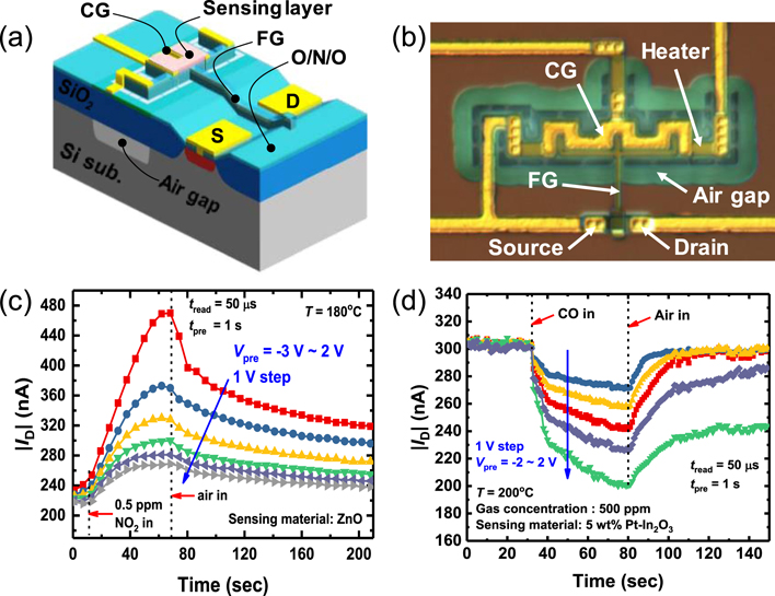
Figure 35. (a) Schematic bird's eye view and (b) top optic microscopic image of the fabricated FET-type gas sensor. (c) Transient |ID| behaviours with different Vpres at 0.5 ppm of NO2 (sensing layer: ALD ZnO) and (d) 500 ppm of CO (sensing layer: Pt-decorated In2O3).
Download figure:
Standard image High-resolution image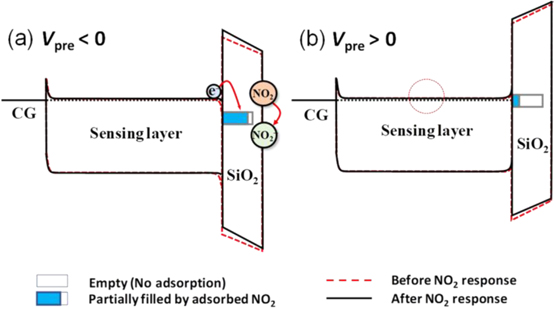
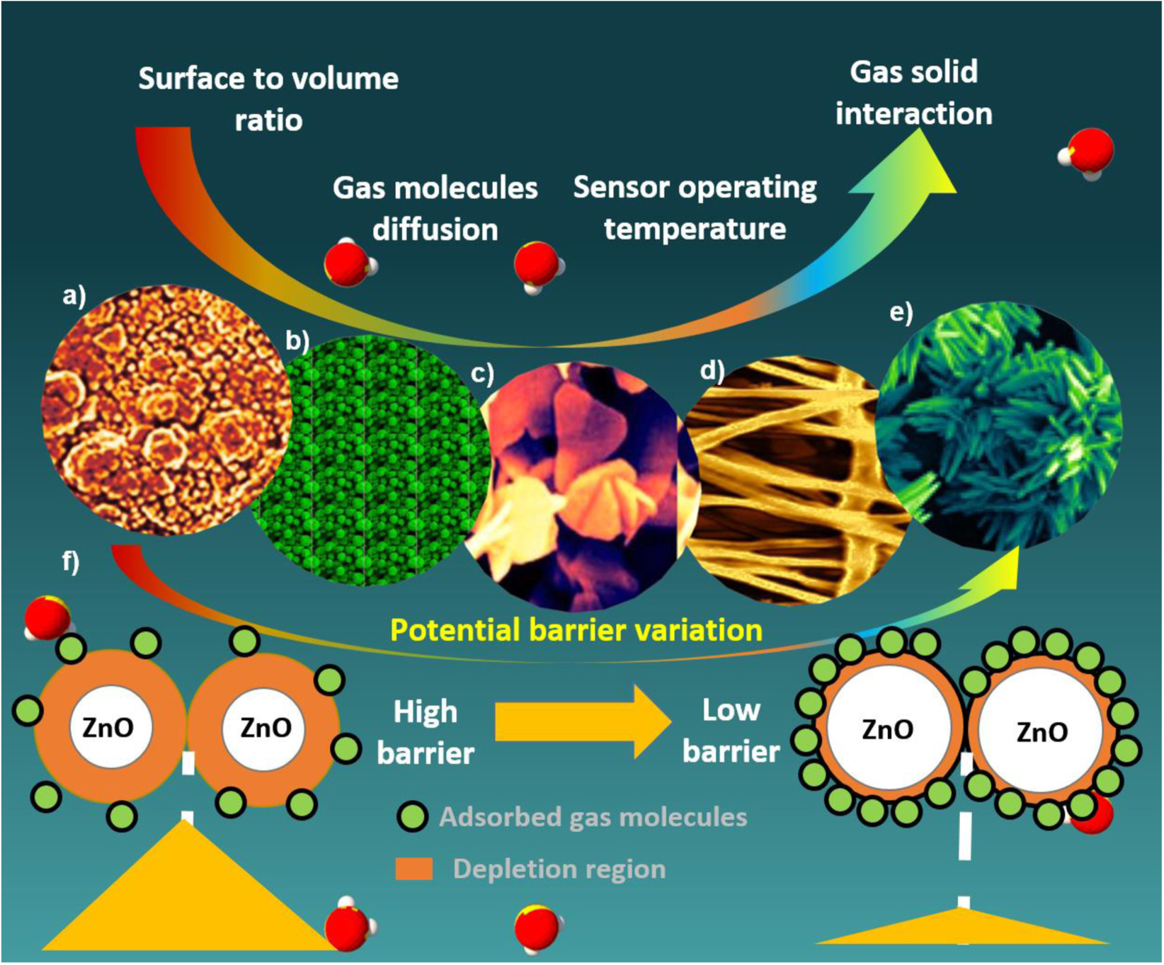
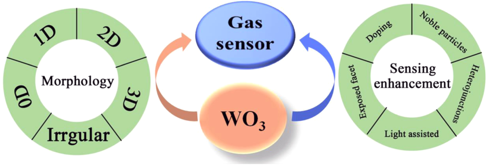
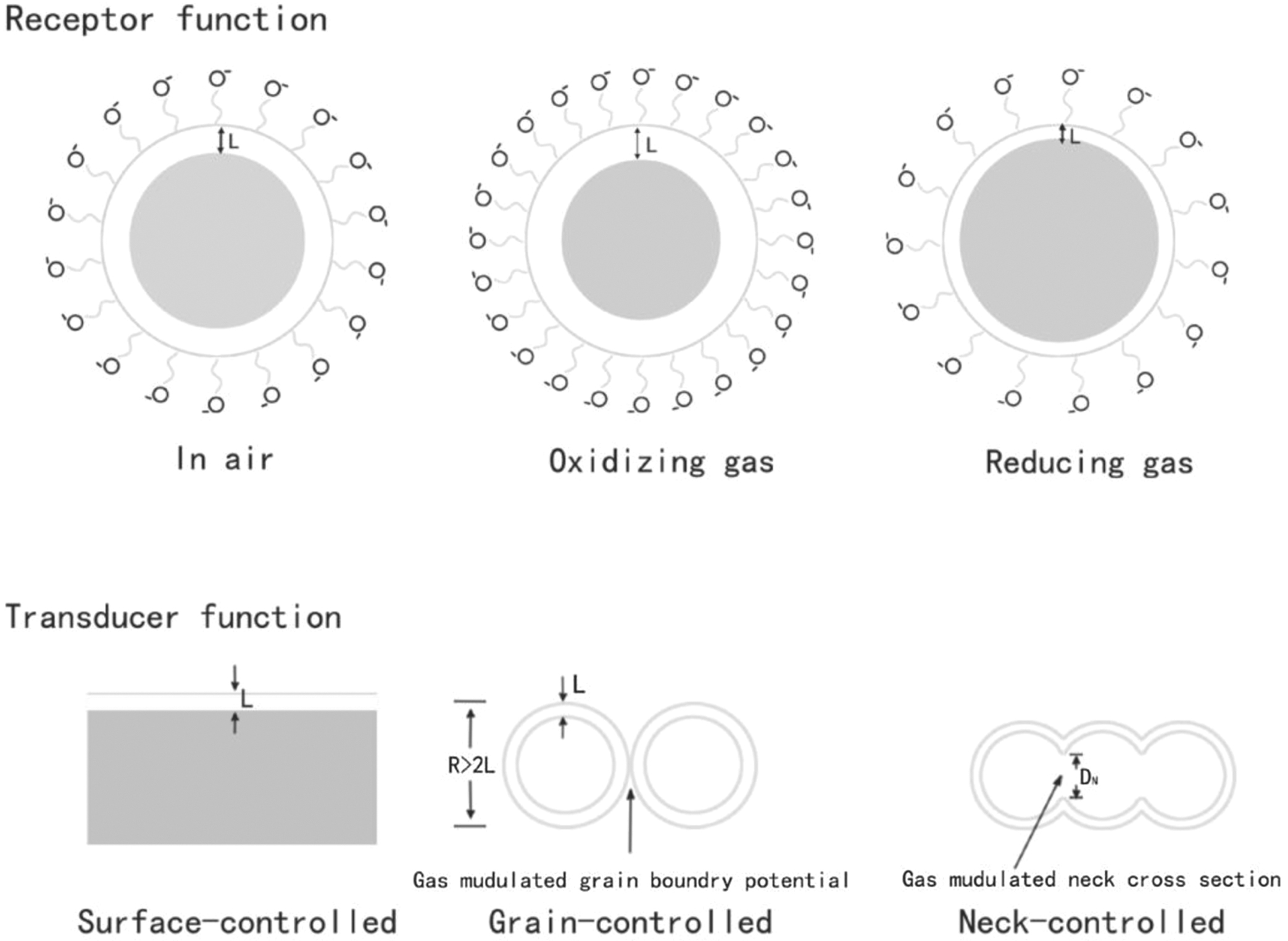
Figure 36. (a) Schematic energy band diagrams of the region along the CG, sensing material and oxide layer in NO2 ambience under (a) a negative Vpre and (b) a positive Vpre.
Download figure:
Standard image High-resolution image
31.2. Current and future challenges
In the FET-type gas sensors, gas selectivity needs to be further improved. The metal doping/decoration process is an excellent candidate for improving gas selectivity. Using catalytic metals, gas sensing characteristics for specific gases are enhanced by the ES and CS in many studies on the resistor-type gas sensors [305]. Thus, the introduction of the metal doping/decoration process to the FET-type gas sensors is expected to improve gas selectivity. Signal-to-noise ratio (SNR), which is critical for resolution and lowest detection limit [306], needs to be analysed in FET-type sensors and reflected in the fabrication process and design of the sensors so that these sensors are optimized. Meanwhile, FET-type gas sensors can be arrayed, and machine learning and neuromorphic networks can be applied to achieve high selectivity and accurate concentration of the targeted gases.
31.3. Concluding remarks
In order to overcome the shortcomings of the conventional resistor-type gas sensor, our group has proposed and continued to develop horizontal FG FET-type gas sensors. In FET-type gas sensors, various kinds of sensing materials have been used to study the gas sensing characteristics of targeted gases. By applying pre-bias (Vpre) pulses before the read operation of the FET-type gas sensor, the sensor's sensing characteristics are greatly affected by the polarity and magnitude of Vpre. This Vpre scheme can greatly improve sensor response and recovery. To improve the gas selectivity of the FET-type gas sensor, metal doping/decoration processes can be introduced into the sensing material. In addition, research is needed to analyse the noise in the FET-type sensor and reflect it in the design to optimize the SNR. Sensors and artificial intelligence need to be combined to accurately detect targeted gases at low power, even in various sensing environments.
Acknowledgments
This work was supported by the Brain Korea 21 Plus Project in 2020 and the National Research Foundation of Korea (NRF-2016R1A2B3009361).
Data availability statement
No new data were created or analysed in this study.