

Abstract
The quasi-two dimensional Coulomb interaction potential in transition metal dichalcogenides is determined using the Kohn–Sham wave functions obtained from ab initio calculations. An effective form factor is derived that accounts for the finite extension of the wave functions in the direction perpendicular to the material layer. The resulting Coulomb matrix elements are used in microscopic calculations based on the Dirac Bloch equations yielding an efficient method to calculate the band gap and the opto-electronic material properties in different environments and under various excitation conditions.
Export citation and abstract BibTeX RIS
1. Introduction
With a thickness of just one unit cell, TMDC (transition metal dichalcogenide) monolayer materials can be viewed as the realization of effectively two-dimensional (2D) system. As revealed by density functional theory (DFT) calculations, the resulting 2D quasi-particle dispersions differ not only quantitatively, but also qualitatively from the three dimensional (3D) bandstructure of the corresponding bulk materials, making these systems interesting both for fundamental material science as well as technological applications. In particular, monolayers of TMDCs and TMDC-based heterostuctures are currently investigated with regards to their application potential in opto-electronic devices. Unlike the bulk TMDC materials, the monolayers display a direct gap in the visible range with strong light matter interaction and many-body effects due to carrier confinement and weak intrinsic screening of the Coulomb interaction [1–5].
A central challenge for the predictive modeling of the TMDC opto-electronic properties is the analysis of the many-body effects and their influence on the optical spectra. Although state of the art, full ab initio GW–BSE calculations have been employed to calculate the linear optical spectra of freely suspended TMDC monolayers, these are numerically extremely challenging and practically intractable for the general nonlinear response. Furthermore, numerical implementations of GW–BSE calculations for quasi-2D TMDCs are artificially 3D and require the insertion of large vacuum regions or truncations of the Coulomb interaction to avoid spurious inter-layer interactions. This not only increases the numerical effort despite decreasing the material's dimensionality, but also limits the applicability to situations where a monolayer is embedded into a more complex heterostucture or photonic crystal cavity. Hence, there is a need for ab initio based theoretical descriptions that are both accurate and flexible to describe the linear and nonlinear optical response under various excitation conditions and different geometries, and at the same allow for the identification and intuitive interpretation of the relevant physical processes.
A powerful tool to compute the optical response of semiconductors for a wide variety of excitation conditions is provided by the semiconductor Bloch equations (SBE), respectively the Dirac Bloch equations (DBE) for TMDCs. Based on the observation that only few bands contribute to the optical response, one derives the equation of motion (eom) for the relevant material parameters from an effective system Hamiltonian including only the relevant valence and conduction bands, thus reducing the numerical complexity enormously. Due to its non-perturbative nature, this approach is particularly well suited to describe the linear and nonlinear optical response in the presence of strong many-body interactions.
As an essential input, the SBE/DBE approach needs the single-particle band structure and the interaction matrix elements. Whereas band dispersions and dipole matrix elements can be either accessed directly from ab initio DFT calculations or from a DFT based model Hamiltonian, the determination of the quasi-2D Coulomb potential and its matrix elements is a nontrivial task. For this purpose, we develop in this paper a parameter-free approach that allows us to efficiently determine the Coulombic input for the SBE from the Kohn–Sham wavefunctions without the need of additional approximations.
The paper is organized as follows: in the following section 2, we briefly summarize the microscopic SBE/DBE approach and introduce an orbital dependent form factor that accounts for the quasi-2D nature of Coulomb interaction potential in TMDCs. We show how this form factor can be computed from the Kohn–Sham wave functions. In section 3, we then provide details of the needed DFT calculations and present a detailed analysis of the form factor. In section 5, we develop an analytic approximation for the form factors that allows us to efficiently calculate the density dependent band-gap renormalization and exciton resonances for different material systems. We discuss and compare our results to available experimental and GW–BSE based ab initio results in section 5.1.
2. Preliminaries
2.1. 2D semiconductor Bloch equations
For a strictly 2D semiconductor, the basic system Hamiltonian is given by

where

describes the single-particle part,
contains the light–matter interaction, and
represents the Coulomb interaction, respectively. Here, ℏ
k∥ is the in-plane crystal momentum, α combines spin and band index,  contains the effective single-particle band dispersion, and
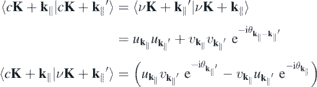
  and
and  denote the momentum and Coulomb matrix elements, respectively. Furthermore,
  is the Fourier transform of the 2D Coulomb potential. In the presence of a dielectric environment, the environmental screening of the Coulomb potential can be included into the definition of the 'bare' Coulomb potential.
The optical response is then given by  and can be computed from the Heisenberg equations of motion for the transition amplitudes
  :
:
Here,


contains the sources and the renormalizations of the single particle energies and internal field. For the interband polarization  , we explicitely have
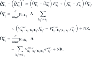
and a similar expression for  . Here, NR refers to nonresonant Auger and pair-creation contributions. As can be recognized, Coulomb renormalizations of the single particleenergies are contained in
  and
and  whereas the attractive electron–hole interaction responsible for the formation of bound excitons is contained in
  . Correlation effects beyond the mean field approximation are contained in

It can be shown that the dominant correlation effect is the replacement of the 'bare' Coulomb potential in equation (3) by its dynamically screened counterpart, yielding the screened Hartree–Fock approximation [6], whereas if correlation effects are neglected, the renormalizations of the single particle energies correspond to the Hartree–Fock approximation.
If the system is excited with an optical pulse of central frequency ωL
, the induced optical current is dominated by transition amplitudes  corresponding to dipole allowed transitions with transition energies
  that are resonant or nearly resonant with the optical frequency. If the relevant bands are sufficiently isolated, one can restrict the microscopic analysis to the resonant transition amplitudes and occupation numbers
  of those bands and the only coupling to remote bands is via screening of the Coulomb potential. Treating screening within the RPA approximation, we can make the separation


Here,  includes all ground state and environmental screening contributions,

contains the optically induced deviations from the ground state polarization function only, and γT is the triplet dephasing rate, respectively. Hence, if the single particle dispersions, optical dipole and Coulomb matrix elements as well as the ground state screening of the Coulomb potential are known from ab initio calculations, the SBE provide a very efficient scheme to compute the optical response since they only need to be solved for a few bands and that part of k∥ space in which populations and/or polarizations are optically induced.
Specifically, for TMDCs it is often sufficient to include the two spin–split valence and conduction bands near the K-points where the single particle dispersion displays a direct gap. Here, the single particle dispersion can be approximated by the relativistic dispersion

that results from the widely used massive Dirac–Fermion (MDF) model Hamiltonian?. Here, i = sτ combines the spin and valley index, Δi , vF,i and EF,i are the spin and valley dependent gap, Fermi velocity and Fermi level, respectively. The occurring parameters can be adjusted to reproduce the DFT bandstructure near the K-points. The overlap matrix elements resulting from the MDF Hamiltonian are
with 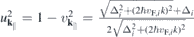 .
.
2.2. Coulomb potential and screening in quasi-2D materials
Although the material excitations in quasi-2D materials are confined to a region |z| ≲ d/2 ⩽ L/2, the Coulomb potential is long ranged and the interaction among particles confined in the layer is sensitive to the dielectric environment. Furthermore, for the evaluation of the opto-electronic system response, one needs the screened Coulomb potential that not only contains screening contributions from the dielectric environment but also all ground state contributions from the material itself.
Within DFT, the macroscopic (3D) dielectric constant is obtained as
where  q
(r) is a lattice periodic function and ⟨...⟩Ω denotes a spatial average over the elementary unit cell. If applied to an artificial 3D crystal consisting of parallel monolayers separated by large vacuum regions, the averaging over a region much larger than the extension of the electron density yields a dielectric function that decreases with the size of the artificial unit cell and hence, cannot be used to construct the screened 2D Coulomb potential [7]. To avoid this complication, we developed in a previous publication [6] an electrostatic model that is based on the bulk dielectric functions which can be directly computed from 3D DFT calculations, thus avoiding any difficulties related to the artificial insertion of large vacuum layers.
q
(r) is a lattice periodic function and ⟨...⟩Ω denotes a spatial average over the elementary unit cell. If applied to an artificial 3D crystal consisting of parallel monolayers separated by large vacuum regions, the averaging over a region much larger than the extension of the electron density yields a dielectric function that decreases with the size of the artificial unit cell and hence, cannot be used to construct the screened 2D Coulomb potential [7]. To avoid this complication, we developed in a previous publication [6] an electrostatic model that is based on the bulk dielectric functions which can be directly computed from 3D DFT calculations, thus avoiding any difficulties related to the artificial insertion of large vacuum layers.
Whereas we refer to reference [6] for a detailed derivation of our electrostatic model, we briefly summarize the most important steps with respect to the screened interaction for further use in this paper (figure 1). As visualized in figure 1, we considered TMDCs embedded in different dielectric surroundings, such as in vacuum, on a substrate and embedded in two different dielectric media.

Figure 1. Illustration of the different dielectric settings considered in the calculations presented in this paper.
Download figure:
Standard image High-resolution image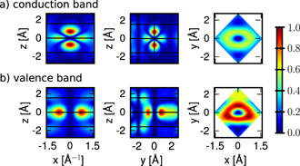
Figure 2. Probability density ρ = |ψ(r)|2 for (a) the conduction and (b) the valence band of MoS2 at the K-point plotted for cuts through the unit cell along the x-, y- and z-axis centered around the molybdenum atom. The black lines indicate the atomic z-position and illustrate the wave function localization in between the chalcogen layers.
Download figure:
Standard image High-resolution imageTo account for the environmental and ground state screening, we consider a slab geometry with
and determine the interaction potential as solution of Poisson's equation. The resulting interaction potential within the slab is given by
with  ,
,  and similar for κT/B and
from which the 2D Coulomb potential is obtained as  . In the last line of equation (8), the first term describes the direct interaction of two electrons located at z and z' whereas the second term describes the interaction with image charges. From equation (8), the 'bare' Coulomb interaction
  , containing environmental screening only, is obtained by setting
  ∥ = ⊥ = 1 within the slab, whereas the true vacuum Coulomb interaction
  is obtained by additionally setting κT = κB = 1. Hence, equation (8) suggests that the Coulomb potential without intrinsic screening can be expressed as
  , where the last term describes the interaction via image charges. Similarly, one obtains the screened Coulomb interaction in bulk,
  , by inserting the bulk parameters for the in- and out-of-plane dielectric constants
  and
and  both within the slab and for the top and bottom environment.
Whereas both  and
and  are independent of the slab thickness L, the interaction with image charges in the presence of environmental screening introduces a dependence on the slab thickness L both for the 'bare' and screened monolayer interaction potential. To model the monolayer potential, we shall assume a slab thickness L = D where D = c/2 is the natural layer-to-layer distance in the naturally stacked bulk crystal. In the long wavelength limitq∥
D → 0 one obtains
are independent of the slab thickness L, the interaction with image charges in the presence of environmental screening introduces a dependence on the slab thickness L both for the 'bare' and screened monolayer interaction potential. To model the monolayer potential, we shall assume a slab thickness L = D where D = c/2 is the natural layer-to-layer distance in the naturally stacked bulk crystal. In the long wavelength limitq∥
D → 0 one obtains  , corresponding to the widely used Rytova–Keldysh potential with a screening length
  that depends on the dielectric contrast between the TMDC material and dielectric environment. In particular, if the dielectric environment is the bulk TMDC crystal itself, the screening length vanishes. For the short wavelengths q∥
L/2 → ∞, the screened potential approaches
that depends on the dielectric contrast between the TMDC material and dielectric environment. In particular, if the dielectric environment is the bulk TMDC crystal itself, the screening length vanishes. For the short wavelengths q∥
L/2 → ∞, the screened potential approaches  , independently of the dielectric environment. Comparison with the bulk Coulomb potential allows us to identify
  and
and  for the ground state screening even in the case of a monolayer. Hence, we can write for the Coulomb potential including environmental and ground state screening

where  describes the screened interaction via image charges. Equation (9) should be compared with the division W = WML + ΔW that has been used in the GΔW approach where ΔW contains the changes in the screened potential as compared to the suspended monolayer [7].
2.3. Form factor to quantify the impact of three-dimensionality
Even monolayer TMDCs have an intrinsic thickness since they consist of three atomic layers and their atomic orbitals have a finite extension perpendicular to the layer plane. Consequently, the Coulomb interaction in these materials differs both from the exact 2D and the three-dimensional cases. Taking the in-plane periodicity and the finite out-of-plane extension into account, a 2D ansatz gives the Bloch states,

with strictly 2D crystal momenta but 3D spatial coordinates r. Hence, the Coulomb Hamiltonian contains the quasi-2D matrix elements
and a similar expression holds for the matrix elements of the screened Coulomb potential.
According to equation (8), the Coulomb interaction differs from the exact two-dimensional potential only in the exponential terms. Hence, we can write for the screened Coulomb potential


Here,
is a form factor and


is its correlated part, respectively. In the 2D limit, the exponential term in the form factor approaches unity and the 2D Coulomb matrix element is recovered due to the wavefunctions orthonormality. Furthermore,  , while for large scattering vectors q∥ → ∞ the form factor approaches 0. Since the potential of the image charges is particularly important in the long wavelength limit where the correlated part of the form factor is negligible, the Coulomb matrix elements of the quasi-2D TMDC structures can be expressed in a good approximation by the exact 2D term modified by the form factor.
2.4. Combined SBE/DFT approach
In the following, we will assume that the single-particle band dispersion and wave functions can reliably be computed from DFT and use the DFT parameters as input for the SBE/DBE evaluations. From a fundamental point, this is in fact a nontrivial assumption. As is well known, DFT is based on the assumption that the two-particle interaction in any given system is a universal functional of the electron density while all system specific contributions to the many-body Hamiltonian are contained in the external potential. Using the dielectric model presented in section 2.2, it becomes clear that the substrate not only changes the screened Coulomb potential but also modifies the 'vacuum' potential that now contains interactions with image charges. Thus, in the presence of external screening, all particles (electrons and ions) interact via a modified Coulomb potential and hence, the electron–electron interaction can no longer be considered as universal.
However, analytical estimates based on the expression for the 'bare' Coulomb potential presented in section 2.2 show that the influence of the dielectric screening on the DFT single particle energies should be small for particles confined to a region |z|≲ d/2 < D/2. Indeed, rigorous treatments of monolayer TMDCs embedded in different dielectric environments have shown that the single-particle bandstructure in the proximity of the direct band gap at the K point remains unchanged for different environments [10]. Therefore, the single-particle bandstructure near the K-point can be obtained from an artificial 3D supercell calculation even in the presence of external screening.
3. Details of DFT computations
For our DFT calculations, we use the plane-wave based code Vienna ab intio Simulation Package (VASP) [11–14] including the core electrons contribution by precalculated projector augmented-wave pseudopotentials [15]. All calculations were performed using the non-empirical generalized gradient Perdew–Burke–Ernzerhof (PBE) functional [16], with additionally including spin–orbit coupling and van-der-Waals interactions by the dispersion correction as proposed by Grimme (DFT-D3) [17].
In a first step, the materials structure was relaxed until remaining forces acting on the atoms were less than 1 meV Å−1. The number of plane waves was hereby restricted by a cutoff energy of 750 eV and convergence was checked with respect to the discretization of the Brillouin zone and the vacuum region that was added in z-direction to prevent interactions between the monolayers despite periodic boundary conditions. For further calculations of electronic properties, the Brillouin zone was discretized by a 12 × 12 × 1, Γ centered k-point Monkhorst–Pack [18] grid and the energy cutoff was set consistently with the precalculated pseudopotentials. In practice, approximately 15 Å of vacuum were included in z-direction.
Using the relaxed structures, the electronic properties were calculated for different paths in the Brillouin zone originating in one of the K points where the direct TMDC band gap is found. The paths were chosen along  in addition to paths of the same length but rotated by 30° and 60° which, due to the hexagonal symmetry, is sufficient to describe the behavior around each K point in steps of 30°.
As the Kohn–Sham wave functions are determined up to an arbitrary phase that can be chosen at each k∥-point independently, we pick the phases such that the intra- and interband matrix elements are given by  and
and  respectively, corresponding to the p ⋅ A gauge. The remaining free global phase is chosen such that bright excitons are predominantly s-type.
3.1. Ab initio wave functions
The finite extension of the electron density in the direction perpendicular to the TMDC plane is illustrated in figure 2(a) for the example of MoS2. Here, the normalized density distribution for both valence and conduction band at the K-point is plotted for different cuts through the unit cell.
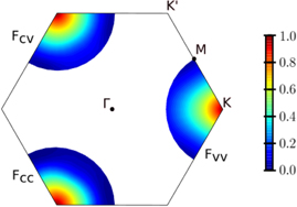
Figure 3. Form factor for inter- and intraband interaction of MoS2 in a range of  0.62 Å−1 around the K-point. As path dependent changes of the form factor are only small, they are approximated as isotropic around the K-point and subsequent calculations are performed using path-averaged form factors.
Download figure:
Standard image High-resolution imageFor MoS2, the wave functions are linear combinations of the transition metal's d-orbitals that are strongly localized in between the chalcogenite layers. While the conduction-band wave function is dominated by the dz
-orbital, the wave function of the valence band is a linear combination of the in-plane dxy
- and  -orbitals [19]. This is different in tungsten based materials where the transition metal's s-orbital and the chalcogen atom's pz
-orbital both have a finite contribution to the conduction or valence band respectively. These features result in a relatively higher density distribution in the tungsten layer for the conduction band whereas for the valence band the density distribution extends farther in the direction towards the chalcogen atoms, respectively.
-orbitals [19]. This is different in tungsten based materials where the transition metal's s-orbital and the chalcogen atom's pz
-orbital both have a finite contribution to the conduction or valence band respectively. These features result in a relatively higher density distribution in the tungsten layer for the conduction band whereas for the valence band the density distribution extends farther in the direction towards the chalcogen atoms, respectively.
4. Analysis of the form factor
4.1. Path-dependency
For the optical response, the properties of the form factor are of interest especially close to the direct band. Therefore, we compute the form factor for scattering vectors  with k∥ fixed at the K-point and
  modified along different paths through the first Brillouin zone. The band structure is similar for all paths close to the K-point but changes significantly farther away, particularly for the conduction band where in the K + 60° direction a secondary minimum can be seen that forms the indirect band gap in the reference bulk structure.
In Figure 3, we show a density plot of the form factor for inter- and intraband interaction in the region around the K-points for the example of MoS2. Despite the anisotropy of the band structure, the MoS2 form factor of the interband interactions Fc
v
decreases isotropically around the K-point up to a range of  0.45 Å−1. The same is true for tungsten based materials, but only up to
  0.30 Å−1. Thereafter, the gradient in K-direction is smaller than in Γ-direction, whereby the absolute differences are less than 0.06. Path dependent differences are larger with regard to the intraband interactions. Here, the gradient is smaller in the direction towards the Γ-point for the valence and towards the M-points for the conduction band, respectively. However, but even here, the form factor is isotropic in a range of
  0.15 Å−1 and absolute differences are always less than 0.12. Thus, the differences occurring for the intraband form factor depending on different orbital compositions of the states seem to balance out in the integration over both valence and conduction band states in the interband form factor. In the following, averages over calculations along different paths are shown and used in subsequent calculations.
4.2. Supercell dependency
In order to be useful, the introduced form factor should be insensitive to the periodic boundary conditions applied in the DFT code and it should be applicable not only to model the Coulomb interaction in monolayers but also in bulk structures. To check these properties, we calculated the form factor for different extensions of the vacuum region included in the supercell.
Our results show that as long as we properly relax the structure before calculating the form factor we obtain similar results independent of the used super cell size. The same is true even if we consider the transition to a quasi-bulk structure differing from the common crystalline structure of MoS2 in stacking order (usually 2H-/3R-phases) and in the interlayer distance by about 0.6 Å. On this basis, we conclude that we can use the determined form factors to model a wide range of mono- and multi-layer systems in different dielectric environments.
4.3. Analytical description
To illustrate the effect of the form factor in real space, we compare in figure 4 the exact 2D and the quasi-2D Coulomb potentials for MoS2. As we can see, the form factor effectively removes the Coulomb singularity at the origin but leaves the potential unchanged for larger distances, i.e., for r∥ ⪆ 7 Å. the slope of the quasi-2D potential approaches that of the original 2D potential.
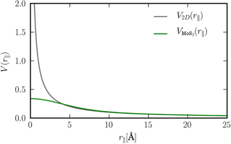
Figure 4. Comparison of the exact 2D Coulomb potential and the quasi-2D Coulomb potential in real space for the example of MoS2.
Download figure:
Standard image High-resolution imageIn figure 5, we show examples of the momentum dependent form factors for inter- and intraband transitions that were numerically evaluated using the full wavefunctions. To simplify detailed calculations on the SBE/DBE level, it is useful to develop analytical approximations for the form factor. For this purpose, we replace the full wavefunctions by their respective values at the K-point and incorporate the orbital dependent overlap matrix elements that occur within the MDF model.
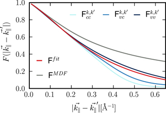
Figure 5. Comparison of the interband (subscript v
c) and intraband (subscripts cc and v
v) form factors together with the analytical approximation (red curve). The grey curve shows  .
.
Download figure:
Standard image High-resolution imageAs shown by the green curve in figure 5, this procedure captures the main features of the full form factors for small scattering vectors. However, for scattering vectors larger than 0.1 Å−1 or 0.2 Å−1 clear deviations are seen such that additional corrections are needed.
In some of our previous works (see e.g. references [6, 20]), we adopted a semi-empirical Ohno potential to account for the finite thickness of the TMDC layers. This approximation has also been used to describe the Coulomb potential of molecules and nanotubes (see references [21, 22]) and was successfully applied in calculations of optical properties of graphene and monolayer TMDCs.
By using the Ohno potential, one regularizes the singularity of the Coulomb potential by introducing an effective thickness parameter d, which in reciprocal space occurs in an additional prefactor  of the Coulomb potential. Even though this ansatz reduces the Coulomb scattering for larger scattering vectors, the detailed analysis shows that it underestimates the form factor for small scattering vectors. Therefore, we additionally introduce an orbital independent exponential function of the form
  , while the orbital dependency is given by the MDF overlap matrix elements. With help of this function, the form factor can be described properly and physically correctly as it approximates 0 for large scattering vectors. Since the orbital dependence is contained in the MDF overlap matrix elements, the orbital independent part can be combined with the strictly 2D Coulomb potential to define the quasi-2D Coulomb potential
  .
.
A physical interpretation of the quadratic contribution can be obtained by considering the real space representation of the quasi-2D Coulomb potential:
Hence, the linear term in the exponent of the form factor changes the pure 2D Coulomb potential into the Ohno potential with thickness d, whereas the quadratic term lead to an additional convolution with a Gaussian of with σ.
4.4. Material dependence of the form factor
In figure 6, we show a comparison of the interband form factor for five commonly discussed examples of semiconducting TMDCs. We notice that for tungsten based materials the form factor decreases slightly faster than for molybdenum based materials. Even more significant modifications occur for different chalcogen atoms. The comparison in figure 6 reveals a more rapid form factor decay when changing from S to Se to Te demonstrating that the gradient becomes steeper with increasing atom size. Since the microscopic distance between the chalcogenide sheets increases with the size of the involved atoms, the systems become slightly more 3D which is reflected in the form factor being a measure for the influence of the finite thickness.
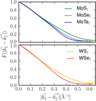
Figure 6. Interband form factors for different (a) Mo based and (b) We based TMDC monolayers. While the general slope is similar for all materials, the decay steepens with increasing size of the respective chalcogenide atoms.
Download figure:
Standard image High-resolution image5. Applications
5.1. Environmental dependent band gap renormalization
As a first application, we calculate the renormalization of the direct K point band gap for different dielectric environments. For the unexcited monolayer, the renormalized band gap is given by

In figure 7, we show the dependency of the gap on the environmental screening for five widely studied semiconducting monolayers (upper part). Since we plot the gap against the inverse value of the substrate dielectric constant, the figure covers the whole range of {1, ∞} and {−∞, −10}. For all materials investigated, we find a similar gap reduction for increased environmental screening. In the lower part of figure 7, we compare the gap shift of the different materials relative to the respective suspended monolayer with and without the form factor included. We note that the shift is almost independent of the form factor. To understand this behavior, we write the equation for the renormalized gap as

and make use of equation (16).
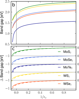
Figure 7. Dependence of the band gap on dielectric substrate screening of the five canonical TMDCs. Here, the limit S → −∞ represents the case of a conducting metallic substrate. The upper part (a) shows the absolute value of the gap, the lower part (b) the shift of the gap relative to the gap of a suspended monolayer with (full lines) and without (dashed lines) inclusion of the form factor.
Download figure:
Standard image High-resolution imageThus, for a strictly 2D system, the gap renormalization is determined by the screened Coulomb matrix elements at r∥ = 0 and z = z' = 0. However, the form factor replaces z = z' = d in the value of the screened Coulomb potential and additionally averages the Coulomb potential over a region around the origin using a Gaussian weight function. Both effects have a significant impact on the direct interaction contained in W2D bulk(r∥) = 1/κr∥ that varies strongly in the region around the origin. In contrast, changes contained in  vary only weakly within the region around the origin and hence are less affected by the form factor.
Furthermore, a comparison of the relative changes for the different materials in the regime of positive dielectric constants shows that these are slightly smaller for Mo rather than for W based materials with maximum differences in the range of few meV. Again, the influence of the incorporated chalcogenide atoms is more significant. Here, the maximum relative differences increase from Te to Se to S based compounds by approximately 80 meV and 45 meV, respectively.
In table 1, we give an overview of the computed band gaps for a variety of TMDCs and different dielectric environments. Comparison with available experimental data shows excellent agreement for all three Mo-based material systems. E.g. for MoS2 we find EG = 2.025 eV for the direct gap at the K-points in bulk, whereas we find EG = 2.473 eV for the freely suspended, EG = 2.279 eV on top of a fused silicon substrate, and EG = 2.160 eV for an hBN encapsulated monolayer. The gap on a metal substrate (e.g. gold) can be estimated from the limit 1/S → 0−, yielding EG = 1.944 eV. These values are in excellent agreement with available experimental data, listed also in table 1. In contrast, the gaps for the W-based materials appear to be 130–150 meV below reported experimental values. Comparison with the MoX2 systems shows that the predicted gaps for the corresponding WX2 and MoX2 are very similar, whereas the experimentally reported WX2 gaps are always above those of the corresponding MoX2 systems under comparable conditions. Since the environmentally induced band gap changes are captured very well by our analysis, we speculate that the origin for the systematic underestimation of the gap in the W-based systems is most likely at the DFT level.
Table 1. Substrate dependent quasiparticle band gap of five semiconducting TMDC systems. The band gap is given for freely suspended, a substrate supported (fused silicon and metal), and hBN encapsulated monolayers. Additionally, literature values based on experimental and/or theoretical investigations are listed for comparison. Here, we distinguish between theoretical GW/GdW calculations building on DFT calculations employing different functionals, namely a local density approach (LDA), the generalized gradient approximation parametrized as by PBE or the hybrid functional Heyd–Scuseria–Ernzerhof (HSE). Additionally, results based on the GVJ-2e approach are summarized. Furthermore, concerning experimental results, we distinguish between photoluminescence (excitation) [PL(E)] measurements yielding the optical band gap from which the quasiparticle gap is extrapolated on the basis of a model for the exciton resonance energies, and scanning tunneling spectroscopy (STS) and angle-resolved photoemission spectroscopy (ARPES) measurements.
| Material | Substrate | Eg (eV) | Theor. | Exp. | |||
|---|---|---|---|---|---|---|---|
| LDA + GW/GdW | PBE/HSE + GW/GdW | GVJ-2e | PL/PLE + model | STS/ARPES | |||
| MoS2 | 2.473 | 2.8 [10], 2.9 [23], | 2.55 (@300K), | 2.38 [25] | |||
| 2.63 (@0 K) [24], | |||||||
| 2.53 [26], 2.62 [27], | |||||||
| 2.54/2.65 [28] | |||||||
| SiO2 | 2.279 | 2.17(4) [29] | |||||
| hBN encaps. | 2.16 | 2.16 [30], | |||||
| 2.146 [29] | |||||||
| Au | 1.945 | 2.3 [10] | 1.95(5) [32], | ||||
| 1.90 [33] | |||||||
| MoSe2 | 2.111 | 2.6 [23], 2.26 [34], | 2.12 [26], 2.24 [35] | 2.03 [25] | |||
| SiO2 | 1.941 | ||||||
| hBN encaps. | 1.835 | 1.874 [30] | |||||
| Au | 1.628 | ||||||
| MoTe2 | 1.57 | 1.72 [35], 1.72 [36] | |||||
| SiO2 | 1.444 | ||||||
| hBN encaps. | 1.356 | 1.352 [30] | |||||
| Au | 1.166 | ||||||
| WS2 | 2.41 | 2.81 [23] | 2.53 [26], 2.83 [35] | 2.51 [25] | |||
| SiO2 | 2.206 | 2.73 [37], 3.01 [38], | |||||
| 2.37 [3], 2.40 [39] | |||||||
| hBN encaps. | 2.084 | 2.238 [30] | |||||
| Au | 1.877 | ||||||
| WSe2 | 2.063 | 2.4 [23] | 2.35 [40] | 2.11 [25] | |||
| SiO2 | 1.885 | 2.63 [38], 2.35(20) | 2.38(6) [29] | ||||
| [41], 2.02 [5] | |||||||
| hBN encaps. | 1.777 | 2.22 [40] | 1.884 [42], 1.890 [43] | ||||
| Au | 1.573 | 1.75 [33] |
For the suspended monolayers, we can also compare our results with other ab initio methods. Reported quasi-particle gaps based on the GW/GdW approach vary over a wide range of up to 400 meV and we find our results at the lower end of this spectrum. Regarding the relative differences in the gaps of the W- and Mo-based monolayers, the LDA and PBE based GW results show the same trend as our results, namely almost equal gaps for the sulfides and the selenides, thus supporting the assumption that the systematic discrepancy for the WX2 originates at the DFT level. Regarding the shifts of the band gap with increased dielectric screening, our results agree well with the available GW-based predictions.
5.2. Density dependent band gap renormalization
As a second application, we calculate the band gap renormalization resulting from finite carrier densities in different TMDCs. In the presence of excited carriers, the renormalized band gap
contains the dynamically screened Coulomb matrix elements  , that, in turn, contain the renormalized single particle dispersions
  . These equations are solved self consistently together with equation (6), assuming thermal carrier distributions at 300 K within the renormalized bands. Here, we distinguish between optically excited carrier densities (equal numbers of electrons and holes) and carrier densities due to doping, where we restrict the analysis to electron doping only. In the presence of excited carriers, both, screening of the Coulomb potential by the excited carriers and phase space filling contribute to the conduction and valence band renormalization. In contrast, for the case of electron doping, the valence band renormalization is solely due to screening effects corresponding to the Coulomb hole, whereas the phase space filling effects additionally contribute to the conduction band renormalization.
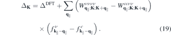
The interplay between phase space filling and screening contributions sensitively depends on the employed screening model. In particular, the approximation of static screening leads to an overestimation of screening effects. To show the importance of dynamical screening, we compare the band gap of a SiO2 supported MoS2 monolayer in figure 8 for different carrier excitation conditions. Using the static approximation for the screened Coulomb interaction, the gap decreases very rapidly with increasing carrier density. Here, the decrease depends only little on the fact whether the carriers are generated by optical excitation or doping, indicating that the gap renormalization is completely dominated by the Coulomb hole. In contrast, for the case of dynamic screening, the gap decreases more slowly with increasing carrier density and is larger for the symmetrical, optically induced electron–hole densities than for electron densities alone.
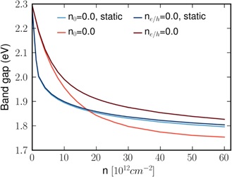
Figure 8. Comparison of the band gap renormalization in dependence of the carrier density n for static and dynamic screening for the example of a quartz supported MoS2 monolayer. Here, n0 = 0 indicates the absence of doping and ne/h = 0 denotes the absence of optically excited carriers, respectively.
Download figure:
Standard image High-resolution imageUsing the dynamical screening calculations, we compare in figure 9 the density dependent gap for the five investigated monolayer materials assuming optically induced electron–hole densities (solid lines) and electron densities only (dashed lines). Whereas the overall behavior is similar in all materials, the effects are somewhat more pronounced in Mo than in based systems, also increasing from S to Te. Furthermore, the renormalization depends on the distribution of carrier densities, thus the band gap changes are weaker due to doping densities than due to optically excited carriers. This effect is more pronounced in than in Mo based materials.
Figure 9. Dependence of the band gap renormalization on the carrier density for dynamical screening with γT = 100 meV for different transition metal dichalcogenides. Solid lines mark calculations with n0 = 0 cm−2, dashed lines belong to calculations with ne/h = 0 cm−2.
Download figure:
Standard image High-resolution imageFinally, we compare the influence of excited carriers on the band gap of MoS2 for different dielectric environments in figure 10. As we can see, the environmentally induced band gap offset vanishes rapidly with increasing carrier density, showing that density dependent screening effects dominate the band gap over dielectric screening effects for moderate to large carrier densities.

Figure 10. Dependence of the band gap renormalization on the carrier density for dynamical screening with γT = 100 meV for different MoS2 in different dielectric environment, namely SiO2 supported or hBN encapsulated.
Download figure:
Standard image High-resolution image5.3. Exciton resonances and binding energies
As third and final application, we calculate the resonance energies of the A exciton series for different TMDCs in various dielectric environments. Similar to the band gap renormalization, we find that the exciton binding energy decreases due to enhanced screening of the Coulomb interaction in media with increased dielectric constant. For the 1s exciton, the decrease in the band gap renormalization and binding energy nearly cancel. As a net result, the 1s exciton shows only a small red shift with increased dielectric screening. In contrast, for the higher exciton states, the band gap renormalization dominates over the decreased binding, yielding a pronounced red shift of the excited states with enhanced dielectric screening.
As representative examples, we show in figure 11 the excitonic resonances generated by solving the Dirac–Wannier equation for MoS2 and WS2 on a quartz substrate and for an hBN encapsulated configuration. Here, the four energetically lowest resonances are shown together with the quasiparticle band gap. As mentioned earlier, the gap of the W-based systems is systematically underestimated such that we have to shift the DFT gap by 149 meV for WS2 while keeping the dipole matrix elements constant BEFORE we compute the renormalizations and exciton binding energies. While the band gap decreases from the SiO2 to the hBN encapsulated sample by about 110 meV, the 1s resonance energy decreases only by less than a fourth of this amount. Thus, the binding energy is reduced by about 90–100 meV for WS2 and MoS2 respectively. In contrast, the binding energies of the 2s, 3s, 4s excitons are reduced by 40 − 20 meV only.

Figure 11. Resonance energies of the A exciton series and quasiparticle band gap for MoS2 and WSe2 at a SiO2 substrate (left) and hBN encapsulated (right) as illustrated in the above sketch. Colored symbols mark our results. Experimental values were taken from 28, 29, 34, 39–44 and are shown for comparison (grey symbols). As for WS2 the band gap is underestimated in DFT calculations, we shifted the DFT gap for WS2 by 149 meV while keeping the dipole matrix elements constant. For both materials, the exciton resonances are in acceptable agreement with experimentally derived values.
Download figure:
Standard image High-resolution image
6. Summary and conclusions
In summary, we investigated the effectively quasi-2D nature of the Coulomb interaction potential in TMDC monolayers. We compute the matrix elements at the K-points of the Brillioun zone and introduce a form factor that effectively captures the deviations from the corresponding ideally 2D case. We apply this concept to efficiently compute fundamental properties such as excitonic resonances and density-dependent band gap renormalizations for a range of TMDC monolayers in different dielectric environments and under various excitation conditions.
Comparing our results both to current experimental data and theoretical approaches based on GW/GdW–BSE calculations, we obtain good quantitative agreement as summarized in table 1. In particular, our computed dependence of the band gap dependence on the dielectric surrounding is qualitatively in good agreement with the GdW based study of Riis-Jensen et al [47]. Also the comparison with experimental data yields excellent agreement for the quasiparticle band gap of all Mo based materials.
For the W based systems, the experimentally obtained values vary in a wide range with differences up to 600 meV. Using the DFT results as an input, our computed band gaps are about 100–200 meV below most experimental values. Interestingly, it can be observed that results based on the PBE functional tend to be below results using an LDA functional. Thus, the choice of the XC-functional has an impact on the absolute band gap value and absolute differences may result from an underestimation of the band gap in the DFT calculations. Fitting the underestimated DFT gap for subsequent calculations for WS2-systems but maintaining the gap unchanged for MoS2-systems, we find an acceptable agreement of the A exciton series with experimental data, see figure 11. Furthermore, our approach reproduces the experimentally observed influence of the dielectric environment.
To illustrate the usefulness of our approach for the excitation dependent system properties, we compute the modifications induced by charge carriers on the dynamic band gap renormalization. In experimental studies, this effect has been analyzed by employing electrical gating, examining the influence of doping to the band gap [39, 48], or by pump-probe experiments, using laser pulses to modify the excited electron–hole density in the material [44, 49]. In agreement with experimental observations, our analysis shows that smaller band-gap modifications are obtained in the configuration where additional electrons are introduced by doping relative to the case where symmetrical electron–hole populations are generated by optical excitation.
Acknowledgments
This work was supported by the Deutsche Forschungsgemeinschaft via the Collaborative Research Center 1083 (DFG:SFB1083) and the GRK 1782 'Functionalization of Semiconductors'. Computing resources from the HRZ Marburg are acknowledged.
Appendix.: Material parameters
In table 2 we summarize the DFT based parameters used to model the dielectric and optical material properties near the respective K-points. While the bulk dielectric constants ⊥,  and interlayer distance are direct results of DFT calculations, the band gap Δsτ
, the valence band splitting 2λv
, and der Fermi velocity ℏvF are determined by fitting the DFT band structure. The back ground dielectric constant ∥ is derived in dependence of the bulk value as
and interlayer distance are direct results of DFT calculations, the band gap Δsτ
, the valence band splitting 2λv
, and der Fermi velocity ℏvF are determined by fitting the DFT band structure. The back ground dielectric constant ∥ is derived in dependence of the bulk value as  [6] where χL
(q∥, ω) is the contribution of upper spin–split valence and lowest conduction bands to the total longitudinal susceptibility.
[6] where χL
(q∥, ω) is the contribution of upper spin–split valence and lowest conduction bands to the total longitudinal susceptibility.
Table 2. MDF model parameters for different TMDCs based on DFT calculations using the PBE functional, namely the spin- and valley dependent band gap Δsτ
, the spin splitting 2λv
, the dielectric constants for bulk materials  , ⊥ and the bulk interlayer distance d resulting directly from the calculations. Fermi velocity ℏ
vF and in-plane dielectric constants ∥ are derived from the band structure and the bulk value, respectively.
, ⊥ and the bulk interlayer distance d resulting directly from the calculations. Fermi velocity ℏ
vF and in-plane dielectric constants ∥ are derived from the band structure and the bulk value, respectively.
| Material | s ⋅ τ | Δsτ (eV) | ℏ vF (eVÅ) | λv (eV) |

|
∥
|
⊥
| d (Å) |
|---|---|---|---|---|---|---|---|---|
| MoS2 | + | 1.682 | 3.532 | 0.146 | 15.19 | 11.65 | 6.38 | 6.18 |
| − | 1.831 | 3.467 | ||||||
| MoSe2 | + | 1.41 | 3.027 | 0.183 | 16.72 | 12.81 | 7.81 | 6.52 |
| − | 1.614 | 3.001 | ||||||
| MoTe2 | + | 1.017 | 2.526 | 0.214 | 20.30 | 15.43 | 10.9 | 6.99 |
| − | 1.266 | 2.574 | ||||||
| WS2 | + | 1.626 | 4.433 | 0.428 | 13.98 | 10.56 | 5.93 | 6.22 |
| − | 2.022 | 4.208 | ||||||
| WSe2 | + | 1.385 | 3.941 | 0.46 | 15.58 | 11.81 | 7.65 | 6.51 |
| − | 1.801 | 3.757 |