

Abstract
We present a general unfolding method for the electronic bands of systems with double-periodicity. Within density functional theory with atomic orbitals as basis-set, our method takes into account two symmetry operations of the primitive cell: a standard expansion and a single rotation, letting to elucidate the physical effects associated to the mutual interactions between systems with more than one periodicity. As a result, our unfolding method allows studying the electronic properties of vertically stacked two-dimensional homo- or heterostructures. We apply our method to study  single-layer graphene,
  twisted single-layer graphene, and
  graphene-
  tungsten disulfide heterostructure with an interlayer angle of
  . Our unfolding method allows observing typical mini gaps reported in heterostructures, as well as other electronic deviations from pristine structures, impossible to distinguish without an unfolding method. We anticipate that this unfolding method can be useful to compare with experiments to elucidate the electronic properties of two-dimensional homo- or heterostructures, where the interlayer angle can be considered as an additional parameter.
Export citation and abstract BibTeX RIS
1. Introduction
Vertically stacked two-dimensional (2D) systems with van der Waals (vdW) interactions have fascinating physical properties and potential applications in optoelectronics, electronic transport [1], among other fields. In principle, these 2D-vdW structures should preserve the physical advantages of their pristine monolayers but also allow for achieving unusual and even superior properties, which cannot be obtained otherwise [2]. Besides the atomic composition of each monolayer, the vertical stacking adds a new parameter: the interlayer rotation angle ( ). In general, when two vertically stacked monolayers of the same composition (a homostructure) have a
  , a Moiré pattern is formed, being its commensurable area inversely proportional to
  [3]. In contrast, two vertically stacked monolayers of different atomic composition (heterostructure) also exhibit a Moiré pattern just by the condition of a lattice mismatch of layers [4]. In this sense, different theoretical and experimental groups have reported new physical properties exhibited by two vertically stacked graphene (G) layers related to
  , including optical activity [5], topological edge states [6], and a Mott insulator-to-superconductor transition at a critical
  [7, 8]. Besides bilayer G, the vertical stacking of transition metal dichalcogenides (TMDCs) with G have been considered promising materials for the design of new electronic, optoelectronic, and photonic devices, in particular based on tungsten disulfide (WS2) or molybdenum disulfide (MoS2) [5, 9–13], both layered semiconductors with a direct band gap for single layer.
Through first-principles methods, for instance, based on density functional theory (DFT), it is possible to study the electronic properties of these novel 2D materials, where the use of periodic boundary conditions is highly desirable to reduce the computational effort. However, periodic boundary conditions require matching of the lattice constants of vertically stacked layers to construct a commensurate supercell (SC) of the bilayer heterostructure, such that each layer can be built by a conventional or non-conventional SC. By definition, a conventional SC is constructed just by expansion symmetry operations on the primitive cell (PC), while non-conventional SC requires expansion and rotation operations. In consequence, SC method is a common practice in periodic DFT calculations, making available the study of systems with thousands of atoms, different composition, impurities, vacancies, or combined systems, including vertically stacked 2D-vdW heterostructures with  .
.
Nevertheless, the use of SCs leads to an artificial folding of the electronic bands as a consequence of the reduction of the reciprocal space [14]. Such folding effects hide the real physical interactions, usually leading to a misinterpretation of the results in the Brillouin zone (BZ) of the SC. Indeed, the comparison between the theoretical electronic band structure of SC and angle-resolved photoemission spectroscopy (ARPES) measurements is quite difficult [15]. A successful technique to unveil the change of electronic structure, hidden by the use of SC method, is the band unfolding approach (hereafter, unfolding for simplicity), which has been developed as a post-processing tool for DFT [16–21] and tight-binding calculations as well [22–24]. In the unfolding method for DFT, the calculated Kohn–Sham orbitals of SC are unfolded onto the original BZ of the PC. This technique projects the electronic states from the BZ of the SC to the BZ of the reference system by assigning a spectral weight, Wk(I), where k is a point on the reciprocal space of the SC and I denotes Ith electronic band to be unfolded. Consequently, Wk(I) quantifies how much of the reference system remains in the perturbed one, for example, when the translation symmetry is lost. However, unfolding methods for DFT calculations have been applied only for conventional hexagonal SCs [20, 21, 25]. In contrast, unfolding methods for tight-binding calculations have been improved for hexagonal and non-conventional SCs, and applied to twisted systems [16, 26].
Therefore, we present an unfolding method to analyze the electronic structure of 2D-vdW twisted systems under the scheme of DFT with atomic orbitals as basis-set. Our method is an extension of previous work of [27] and [28], allowing the unfolding of electronic bands of structures constructed by conventional and non-conventional SCs. Hence, it reveals the effective electronic bands (EEBs) of 2D-Moiré structures, unfolding the bands onto either pristine layer. To show the potentiality of the method, we investigate the electronic band structure of two ideal G single-layer with periodicities  and
and  . Furthermore, the electronic band structure of a twisted G-WS2 bilayer with
  is unfolded using our method, unveiling the physical consequences of the mutual interactions between G and WS2 layers. The content of the paper is organized as follows. In section 2, we present a brief description of the unfolding method. Section 3 shows the models studied here to validate our method. Section 4 summaries the computational details employed in the DFT calculations. Then, in section 5, we use our method to unfold the electronic band structure of the SCs described above. Finally, in section 6 we discuss our main conclusions.
2. Method
Under the scheme of DFT with a linear combination of atomic orbitals (LCAO) as basis-set and using Bloch's theorem, the total wavefunction of a system is:
where the sum in  extends to all basis orbitals in space, I labels the different bands, and
  corresponds to the expansion coefficients of the Kohn–Sham orbitals obtained by the self-consistent calculation. The base of our unfolding method stands on the calculation of the spectral weight, Wk(I) which quantifies the projection of the electronic state from the BZ of the SC to the BZ of the PC for the Ith band. Hence, following the development of Deretzis [27], Wk(I) is obtained as:
where both sums on c coefficients run over all the equivalents orbitals j of the  times repeated PC, and over all atoms u with equivalent positions in SC with respect to PC. Here, c is a complex number and
  represents its complex conjugate, and
  is an integer defined as
  , where
  denotes the volume in the real space.
Notice that Wk(I) determines the equivalence of the electronic states of SC on the corresponding of PC and must obey that  , which is true if and only if the basis-set is orthogonal and normalized [27, 28]. For SC with more than one periodicity or built by more than one PC, for instance, any vertically stacked heterostructure, it is necessary to define on which PC the electronic states will be projected. A wrong choice on the PC could induce a bad interpretation on the unfolded bands or even ghost states [26]. Once the PC has been defined, the problem of identify the equivalent u atoms in SC is directly solved because the layer was constructed by expansion and rotation symmetry operations on the PC, which involves an affine transformation between SC and PC. This transformation consists of two parts: a shift of the origin and a linear part. The former is given just by a straight translation of the lattice vectors of PC (
 ,
,  ,
,  ), while the latter implies a change of their orientation, length or both. Through just by a linear transformation, the lattice vectors of the SC (
 ,
,  ,
,  ) are defined by:

with  , a transformation matrix, defined as:
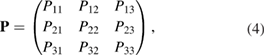
where Pmn are positive integer values and the absolute value of the determinant of P corresponds to  . Notice that Pmn can be parametrized in terms of two or three integer values whether the transformation is carried out in 2D or 3D, respectively. Therefore, the equivalent u atoms of the SC from PC is easily obtained through equations (3) and (4).
This method can be easily generalized to any 1D, 2D, or 3D periodic SC just by the P matrix. However, we focus the following description on the 2D-hexagonal lattice because we are interested in layered systems defined by this symmetry, which are under intense research nowadays. For 2D hexagonal lattice, any conventional or non-conventional SC can be set up using the transformation matrix  , considering c vector as an invariant [29]. Thus, Pmn elements in equation (4) are P33 = 1 and
  . Finally, the other elements are functions of two integer parameters, m and n to take into account expansion and rotation operations. Then, the matrix transformation,
  , simplifies to:
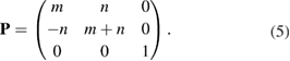
Notice that if m or n = 0, then the 2D hexagonal SC is a conventional one, while a non-conventional SC is obtained for  . For our purpose, given a 2D SC, it is necessary to identify which of the atomic positions are equivalent to the PC. This is solved by a process which follows the inverse process described above to set up a SC from a PC. Additionally, because commonly DFT calculations are carried out including a structural relaxation, it is necessary to specify a threshold value to determine whether an atom has deviated from its initial position or not.
Another important issue for the calculation of Wk(I) is the scanning of the BZ along specific paths of the SC and their projections on equivalent paths of the BZ of PC [27, 28]. In general, the fractional coordinates ( ) of any point in the reciprocal space of PC transform in similar way as the lattice vectors, or any point in the real space, do [29]. Therefore, points in the reciprocal space of SC (
 ) are related with equivalent points in the reciprocal space of PC by an equivalent transformation given by equation (3) and the transformation matrix defined in equation (4):

For a 2D hexagonal lattice,  and
and  is defined through equation (5).
Finally, we can calculate the electronic states of commensurate 2D Moiré SCs with the new coordinates ( ) based on periodic DFT, and thereafter, we can apply the unfolding described above to calculate Wk(I), obtaining the SC projected band structures onto the original PC systems. Since we are performing DFT calculations with a non-orthogonal basis-set [30], we employ a Gram–Schmidt process [31] to orthogonalize the Kohn–Sham orbitals and carry out the unfolding process through the calculation of Wk(I) via equation (2). We want to stress that our unfolding code reads the whole information of wavefunctions from the corresponding siesta file and, then, performs the Wk(I) calculation. Beside with the linear scaling [30], siesta code has different advantages: the choice of the basis-set size, different subroutines for writting the wavefunctions file, and the setting of how many k points will be calculated. Putting all this together, our unfolding code is able to work efficiently for twisted systems with significant number of atoms [27] with respect to other unfolding DFT methods based on plane-waves [20, 21], being able to unfold the electronic states even from the 1st occupied band up to the Ith desired band and improving the resolution of projected band structure easily by the number of k points along the paths.
3. Models
In order to show the validity and main characteristics of the present unfolding method, we study three structures: a conventional SC of monolayer G, a non-conventional SC of monolayer G, and a twisted bilayer G-WS2 heterostructure. First, let us describe the cases of monolayer G. Lattice vectors of the PC are a = aG(1,0,0),  and
and  , where aG = 2.44
  is the lattice parameter optimized through DFT calculations, which is in very good agreement with other reports [5, 32], and c is the vacuum space imposed for the SC (see the computational details in section 4). Conventional and non-conventional SC of monolayer G have a
  and
and  periodicity, respectively. They are constructed using equations (3) and (5) with m = 3 and n = 0 for
  G with
  , and m = 3 and n = 1 for
  G with
  . Inset of figures 1(a) and (d) show both SC. Hence, the total number of atoms, NT, defined as
  , are 18 and 26 atoms, respectively. In general, the rotation angle,
  , between two hexagonal layers is defined as:
where m and n indexes correspond with one of the rotated layer, whereas p and q correspond with the other one. Taking one of the layers as a conventional SC,  and q = 0, the equation (7) simplifies:
giving  .
.
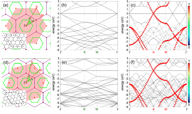
Figure 1. Top row: analysis of  G SC. (a) Reciprocal space of
  G SC. Green hexagons denote the first BZ of G SC, while the shaded-red hexagon does the first BZ of G PC. The filled-green (red) triangle encloses the irreducible BZ of SC (PC). High symmetry points are colored in green (red) for the SC (PC). Inset shows the stick representation of
  G layer in the real space and the dashed-black lines delimit the size of PC: (b) Calculated band structure of
  G SC. (c) Electronic states of SC (gray background) projected onto the red path described in (a). They are plotted with circles of different size and color, which are proportional to Wk(I). Bottom row: (d)-(f) show the corresponding plots for
  G SC. The number of k-points scanned along Γ-K, K-M and M-Γ are 30, 15, and 30, respectively. Wk(I) is proportional to symbol size, and also to the color scale. Fermi level is set at 0 eV.
Download figure:
Standard image High-resolution imageNow, let us describe the case of twisted G-WS2 bilayer. PCs of G and WS2 have hexagonal symmetry; hence, both PCs exhibit the same lattice vectors but different lattice parameter (see figures 2(a) and (b)). Letting an optimization of the lattice parameter of WS2, we obtain 
 , which is in very good agreement with other reports [33, 34]. Since the PCs of G and WS2 have different lattice parameters, the construction of a periodic vertically stacked SC of G-WS2 is an additional problem. To overcome this problem, it is necessary to find SC of G and WS2 with similar lattice parameters; then, one of the layers is fixed and the other one is enlarged or reduced to assure commensurability. In our case, we fixed WS2 as the substrate and G is slightly enlarged or shrunk to match both lattice parameters of SCs. Thus, the in-plane strain (
 ) imposed in G and associated to commensurability condition is an intrinsic property, defined as [35]:
where m and n indexes correspond to G, while p and q do to WS2, obeying the following constrains:  and
and  and
and  % [35]. Then, we employ the matrix transformation described in equation (5) with m = 2, n = 2 for G, and p = 2, q = 1 for WS2, plus the lattice vectors of G and WS2 to generate the periodic SC of G-WS2, shown in figure 2(c). For these indexes,
  %, where the minus sign means compression of the G layer, the twisted-angle
  , the lattice parameter of the SC is 8.34
  , and the total atoms of the SC is 45. Visualization of atomic models was performed using the vesta program [36].
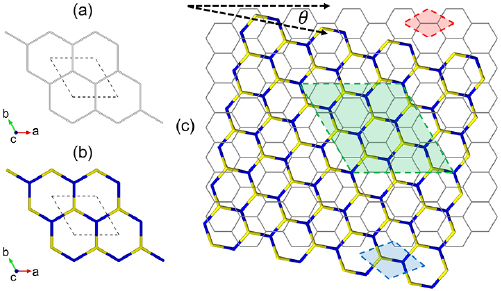
Figure 2. Stick representation of the PC of (a) G, (b) WS2 and (c) the SC of G/WS2, all in a top view. PCs in (a) and (b) are indicated by dashed lines. In (c), the SC of G/WS2 is highlighted by the green area, while PCs of G and WS2 are denoted in red and blue areas, respectively. θ is the angle between the armchair edges of both layers. Color code: gray, yellow, and blue sticks represent C, S and W elements, respectively.
Download figure:
Standard image High-resolution image4. Computational details
DFT calculations are performed using the siesta code [30]. Exchange-correlation energy is described by local density approximation (LDA) with the Perdew–Zunger parametrization [37]. Norm-conserving pseudopotentials [38] in their scalar relativistic and non-local form [39] are employed for electron–ion interactions. The expansion of the valence electronic states is described by a LCAO with an optimized double- polarized (DZP) basis-set plus diffuse orbitals [40–42]. If the basis-set uses strictly localized orbitals, it is necessary to include diffuse orbitals for a better description of interface and vacuum regions in slabs and surfaces [40]. The electronic density is sampled by a mesh-cutoff energy of 300 Ry and converged up to 10−5. The Monkhorst–Pack scheme [43] is used for sampling the BZ with an optimal
  k-grid. Energy mesh-cutoff and k-grid convergence tests were performed leading to the above mentioned values as the optimal ones. A Fermi–Dirac smearing of 1 K is adopted to obtain convergence. The structural optimization is carried out within the conjugate gradient algorithm with a maximum value of 0.01 eV
  for the interatomic forces, as well as 0.5 GPa in the stress components. A vacuum space of 55
  is applied to avoid spurious interactions between periodic images along c direction. Finally, all calculations include a dipole correction, as it was suggested by Bengtsson [44], to cancel the artificial electric field induced by the vertical asymmetry of the SC and the periodic boundary conditions.
5. Results
As a first proof of our unfolding code, we study the electronic structure of an ideal  G conventional layer. The reciprocal space, the first BZ and the irreducible BZ of the SC and PC are shown in figure 1(a). Also, the inset presents the
  G conventional layer. Figure 1(b) shows the electronic band structure of the SC. The typical linear dispersion of electronic states of the PC at the Fermi level around the K point is also present in SC but around the
  point. Due to the folding process, many electronic states are merged into the small SC reciprocal space (the green area in figure 1(a)). The irreducible BZ of the PC has the fractional coordinates K
  and M
and M  in terms of the corresponding reciprocal lattice vectors of PC. After the transformation with equations (6) and (4), the new fractional coordinates of high-symmetry points are K
  and M
and M  but in terms of the reciprocal lattice vectors of SC. With this transformation, the highly symmetric points in the reciprocal space of SC can be easily identified in the reciprocal space of PC (see figure 1(a)). When we unfold the electronic states of SC calculated throughout the red path of G (gray band structure in figure 1(c)) onto the PC of G, the fully band structure of the ideal PC is recovered, as it is shown by red circles in figure 1(c), which means Wk(I) = 1. Some unfolded wavefunctions in figure 1(c) have
  along M–
 within −7.5 and −4.5 eV range, given by green circles and the yellow circle along K–M at −7.5 eV, because the wavefunctions are degenerated due to scanned k-points match with Bragg diffractions. However the total summation of Wk(I)s is
  1. This characteristic of our unfolding process allows seeing two main aspects in comparison with previous unfolding methods with DFT [16–21] or tight-binding calculations [22–24]: first, we can determine a relationship between the reciprocal space and possible Bragg diffractions in the band structure; and, second, electronic degeneracy and/or hybridization can be quantified via Wk(I). These capabilities of our unfolding code are owing to the basis-set used and the normalization process and they will be discussed with more details later for the G/WS2 heterostructure.
We performed the same analysis for  G layer with
  . Figure 1(d) sketches the reciprocal space, the first and the irreducible BZ of SC with the same orientation as those in figure 1(a). The inset shows the corresponding SC layer. Again, the typical linear dispersion of electronic states of SC at the Fermi level around the K point is also present. Comparing figures 1(e) and (b), there are more electronic bands (gray lines as background) in the former at a glance. Nevertheless, when the unfolding process is applied using the new fractional coordinates K
  and M
and M  of PC, the fully band structure of PC is again fully recovered, as in figure 1(f) with Wk(I) = 1. An analysis of unfolded bands of figure 1(f) reveals the absence of states with
  , since the coordinates (
 ) of scanned k-points of SC are not the same positions as Bragg points or lines in reciprocal space. Therefore, our unfolding code works for conventional hexagonal SCs, and non-conventional ones as well.
Now we turn to a more complex system: a heterostructure built by two twisted non-conventional SCs. In figure 2(c), the 2D commensurable heterostructure composed of  G and
G and  WS2 with an interlayer rotation angle
  is depicted. Hence, the number of times that the PC is repeated on the SC,
  in equation (2), or equivalently the determinant of P is 12 for G, and 7 for WS2. The optimized average interlayer distance, d, defined as the average distance between carbon atoms of G and upper sulfur atoms of WS2 is d = 3.28
  , in good agreement with previous reports [45, 46]. Average distances of carbon–carbon (C–C), tungsten–sulfur (W–S) and up and down sulfur atoms (Su–Sd) are 1.41, 2.41 and 3.16
  , respectively. The irreducible BZ of PC of both WS2 and G has the same fractional coordinates. Once the transformation is done using equations (6) and (5) on the high-symmetry points, the new fractional positions are K
  and M
and M  for G, and K
  and M
and M  for WS2. Multiplying these new fractional positions by the reciprocal lattice vectors of SC generate the coordinate points of the twisted irreducible BZ of PCs in figure 3(a), where the red labels identify corresponding BZ of G, while blue labels do with WS2.

Figure 3. (a) Reciprocal space of G/WS2 system. The purple hexagon, joined by red points, represents the reciprocal space, while green hexagons represent the first BZ. The irreducible BZ of SC is represented by a shaded green area. Red and blue hexagons denote the first BZ of PC of G and WS2, respectively. Red and blue triangles denote the path of the irreducible BZ for G and WS2, respectively. K and M labels are in green for the G/WS2 SC, while those in red and blue corresponding with the PC of G and WS2, respectively. Γ-point in black is common for the three structures. (b) Electronic band structure of G/WS2 system, with the Fermi level set at 0 eV.
Download figure:
Standard image High-resolution imageUsing the fractional coordinates K  and M
and M  of the SC, we calculated the electronic band structure of the heterostructure G/WS2 scanning the
  –K–M–
–K–M– path, as it is shown in figure 3(b). Close to the Fermi level, the typical linear energy dispersion associated to the Dirac cones of G is observed at the
  point. The preserving of the linear dispersion in 2D van der Waals heterostructures has been reported in other works [32, 35, 47–49] by means of ab initio calculations. Furthermore, close to the Fermi level the degeneracy is broken at the
  –M path, while it is preserved at the
  –K path. For energies lower than −1 eV and greater than +1 eV there are many electronic states associated to G and WS2 as well, which means that the electronic states of G around the Fermi level fall inside the band gap of WS2, confirming that the full system is a semimetal. From a simple analysis of figure 3(b), it is quite difficult to extract more physical information. Nonetheless, applying our unfolding method to the electronic band structure of G/WS2 onto each PC, it is possible to distinguish the physical consequences of mutual interactions among layers.
Let us apply our unfolding code to the G/WS2 structure to project the electronic states to both PC using the corresponding  –K–M–
–K–M– path for G and WS2 (see figure 3(a)). Once the corresponding Wk(I) values are obtained, the EEBs for G and WS2 are plotted, as it is shown in figures 4(a) and (b), respectively. In general, EEBs show large difference and discontinuities with respect to the electronic band structure of pristine PC of G [50, 51] and WS2 [33, 34, 52] as a consequence of Wk(I) is not exactly equal to 1 in every projected band. Such deviations can be easily observed comparing EEB of G in figure 4(a) with the band structure of pristine PC of G in figures 1(c) or (f). This means that the symmetry of each layer reconstruction is not equal to the original symmetry of pristine PC. In particular, the translation symmetry is broken in this 2D G/WS2 heterostructure due to interlayer interaction.

Figure 4. Calculated EEBs of (a) G and (b) WS2 for the G/WS2 structures with an interlayer distance of 3.28 A. EEBs of G and WS2 are projected onto their corresponding PCs. The vertical dashed lines represent Bragg points and lines in the reciprocal space. Fractional values along paths denote diffraction positions in k-space. Minigaps with a different origin from Bragg reflections are indicated by white arrows, while resonance states are indicated by green arrows. The number of k-points scanned along Γ-K, K-M and M-Γ are 200, 100, and 200, respectively. Wk(I) is proportional to symbol size, and also to the color scale. Fermi level is set at 0 eV.
Download figure:
Standard image High-resolution image
Figure 5. Electronic states of G/WS2 structure projected onto the PC of (a) G and (b) WS2. In both plots, red (blue) circles represent G (WS2) states. Notice that EEBs are different depending on the PC that the electronic states of SC are projected. The number of k-points scanned along Γ-K, K-M and M-Γ are 200, 100, and 200, respectively. Wk(I) is proportional to symbol size, and also to the color scale denoted at the top of either plot. Fermi level is set at 0 eV.
Download figure:
Standard image High-resolution image
In the case of G, the unfolding process shows that the Dirac cone around the Fermi level remains unchanged but it is now located at the K point of PC instead of  of SC. Furthermore, it falls inside of the WS2 bandgap. At the Fermi level, there is no bandgap associated to G bands despite the applied symmetrical strain,
  , which is in agreement with other theoretical results for pristine G undergoes a small symmetrical strain distribution [53]. On the other hand, we detected a change in Fermi velocity (
 ) in G by the strain. A slight increase of 1.54% was measured, taking as reference the unfolded band structure of G SC in figure 1(c). The previous
  value was roughly estimated only for carriers in the valence band. Our results are in good agreement with other experimental and theoretical results [53, 54] with potential applications in strain engineering and flexible electronics. For energies below −3 eV in figure 4(a), there are two bands composed of mixed C(2 s,2 p x,2 p y ) orbitals giving a sp2 hybridization. These bands are non-perturbed showing a
  along the full k-path. Thus, since we performed DFT calculations with a localized basis-set, we can extract partial EEBs taking into account only specific orbitals or atoms of the SC [27]. This result reflects the usefulness of the present unfolding code based on atomic orbitals and normalized wavefunctions for studying of any perturbed periodic system. At the energies plotted in figure 4, only bands associated with C(2 p z) orbitals change drastically. It is observed a splitting bands near to
  point at energies around −8 eV, which is similar to the band structure of graphite [55]. Also, different minigaps in the valence bands are observed. Such minigaps observed at low energies are in fair agreement with experimental results of G adsorbed on MoS2 [56, 57], as well as other theoretical calculations [25, 26] with
  . We will discuss more about the formation of minigaps latter. Another advantage of the unfolding method for studying these systems in comparison, for instance, with ARPES [15] technique is that, we can see what happens with the unoccupied states as well. In this case, in figure 4(a) there is not an equal relation of Wk(I) for each wave function (I) and k-point, which means there is a particle-hole asymmetry and, as result of WS2 interaction, the mobility of holes and electrons would behave different in G [24, 58].
Now, let us discuss the unfolding process projecting the electronic states of G/WS2 to the PC of WS2. The direct-transition electronic band gap located at the K point of PC is preserved, which means that, under our methodology, the vertical stacking of G with WS2 does not change the electronic properties of WS2 near the Fermi energy. In the  –K path and around −1.5 eV, a small discontinuity is observed in the last occupied valence band (second unnocupied band), green arrows in figure 4(b). Going down in energy, all electronic bands of WS2 change from −2 eV to −6 eV, which means that W(d) and S(p ) orbitals modify their occupation just by G adsorption. Another interesting result obtained through the unfolding process is the energy splitting about ∼1 eV of the band at
  –K and M–
 path from −7.5 eV to −8.5 eV (see figure 4(b)), also observed in the PC of G (see figure 4(a)), which means an interlayer interaction repulsion between the C(2p z) orbitals of G and S(3p ) and W(5d) orbitals of WS2. Furthermore, it is noticeable that there is a complementary relationship between the two EEBs of G and WS2 around the
  point for energies from −6 eV to −8.5 eV. Wk(I) of G bands (see figure 4(a)) complements the Wk(I) of WS2 (see figure 4(b)), even when the scanned paths are a bit different near the
  point. This complementary characteristic of Wk(I) between two monolayers is another advantage of our unfolding process, in comparison with other unfolding methods based on Green's functions for periodic twisted bilayers [24, 26].
Regarding the electronic minigaps observed in EEBs of G, it is worth pointing out that their number, size and position in this G/WS2 heterostructure with  is greater than other theoretical reports when
  [25, 26]. This means that
  has a strong influence on the electronic properties in 2D heterostructures, as in the case of G bilayer [5–8]. We have identified two kind of electronic interactions. One is related with the electronic gap generation with a direct transition. The other one seems an electronic resonance (or discontinuity) between out-of-plane orbitals of each monolayer. It is possible to identify both behaviors in the EEBs of G. In figure 4(a), the minigaps are observed along the
  –K and M–
 paths and indicated by white arrows, while electronic resonances are detected in the K–M path indicated by green arrows near the M point. Based on the reciprocal space sketched in figure 3, we can say that the gaps located in 1/2 and 0.7 starting from
  K path and those located at 0.22 and near to 1/3 and 1/2 starting from M
  path are Bragg diffractions. The rest of minigaps have a different physical origin. The discontinuity in K–M path looks like an electronic resonance showing coupling between monolayers. The Bragg diffraction in WS2 located at 0.6 (1/3)
  K (M
K (M  ) path shows minigaps around these points for energies from −5.5 eV to −7.5 eV. Also, other minigaps are observed near the K (on left-side) and M points (on right-side) with energy −3.5 eV indicated by arrows. A discontinuity is observed in 0.6
  K path in ∼2.75 eV below the Fermi level. Finally, the number of Bragg diffractions in G is greater than WS2 by the size of BZs of PCs. The origin of all different interactions will be discussed in a future work.
We want to stress that, strictly speaking if both layers do not interact between them, Wk(I) must be equal to 1 as in figures 1(c) and (f). To corroborate this, we analyze the G/WS2 heterostructure with the interlayer electronic interactions almost zero. This condition is possible putting both layers separated by an interlayer distance larger than the equilibrium one d = 3.28  . Hence, using the optimized G/WS2 structure, we impose an interlayer distance of 5.29
  and, from a single-point DFT calculation, the electronic states of the SC are obtained. Then, we applied our unfolding code to project the electronic states to both PC using the corresponding
  –K–M–
–K–M– path for G and WS2, denoted in figure 3(a) by red and blue labels, respectively. Once the corresponding Wk(I) values are obtained, the EEBs are plotted. Figure 5(a) shows with red and blue circles the EEB of G and WS2 projected onto the
  –K–M–
–K–M– path for G, while 5(b) shows the corresponding EEB projected onto the
  –K–M–
–K–M– path for WS2. Analyzing the EEBs of G and WS2 in figures 5(a) and (b), respectively, they are almost entirely recovered since
  in the whole energy range and the scanned k path as well. This is an outstanding theoretical proof which shows that the strong interlayer interaction, given by vdW forces, leads to hybridization and the emerging of minigaps discussed above. However, some Kohn–Sham orbitals show Wk(I) < 1, which is associated to interlayer distortions originated by the structural optimization carried out at d = 3.28
  . Comparing both figures 5(a) and (b), the EEBs of G are quite different as well as corresponding of WS2. Such differences are originated because in figure 5(a) the states of WS2 are projected onto the BZ of G, while in figure 5(b) the states of G are projected onto the BZ of WS2. So, a wrong choice of the k path could induce a misunderstanding or even a bad interpretation of the mutual influence between layers. Additionally, in every plot in figure 5 we can observe only the electronic states from the reference PCs without the presence of additional bands or the so-called ghost bands [26]. This is another advantage of the present unfolding method based on atomic orbitals and DFT. Comparing the EEB of strained G in figure 5(a) with ideal G bands in figure 1(c) around −8 eV and close to
  point, a shift energy of the electronic state is observed, which is directly related with the strain condition of G monolayer. Meanwhile WS2 is a direct bandgap semiconductor at the K point in its PC, see blue circles in figure 5(b).
6. Conclusions
In summary, total energy DFT calculations in combination with an extended unfolding band structure approach have been applied to study conventional and non-conventional graphene supercells, and twisted bilayer of non-conventional graphene and tungsten disulfide supercells. The unfolding method has been implemented in SIESTA package, a DFT code that uses strictly localized orbitals as basis-set and exhibits a linear-scaling of the computational demand. Hence, our unfolding process opens the possibility to study systems built by hundreds or, even, thousands of atoms, making our methodology very attractive to study the EEBs of 2D-Moiré structures and enabling a direct comparison with experimental results, like ARPES spectra. The unfolding method works for periodically twisted systems, showing that, the full band structure of the PC are recovered if ideal supercells of graphene are studied. Furthermore, we addressed the topic of interaction by proximity effects in a system of graphene and tungsten disulfide with double-periodicity. Several advantages of developed method have been presented and the physics of interlayer interactions is easier to explain. When graphene is adsorbed on tungsten disulfide, many electronic interactions arise between monolayers when the interlayer distance is reduced until its optimal value. The results reveal a strong modulation of the electronic structure of graphene by tungsten disulfide due to the relatively weak van der Waals interactions. In graphene, the main contributions are by the orbital normal to the monolayer planes, while the in-plane orbitals form strong bonds without any perturbation. However, around the Fermi level the Dirac cone remains almost unaffected with small changes in the Fermi velocity of the carriers assisted by symmetric lattice strain. The electronic properties of tungsten disulfide are preserved near the Fermi energy, mainly the direct band gap at the same point. The nature of minigaps comes from Bragg conditions in the SC and the interlayer coupling between graphene and tungsten disulfide monolayers.
Acknowledgments
Authors acknowledge the partial support from DGAPA-UNAM project PAPIIT IN109618 and CONACyT project A1-S-39242. FSO acknowledges to DGAPA- UNAM for postdoctoral fellowship. The numerical calculations were carried out in clusters Baktum and Flatland at the Institute of Physics (UNAM).