

Abstract
We have studied the low temperature electrical transport properties of LaxSr1−xCuO2 thin films grown by oxide molecular beam epitaxy on (1 1 0) GdScO3 and TbScO3 substrates. The transmission electron microscopy measurements and the x-ray diffraction analysis confirmed the epitaxy of the obtained films and the study of their normal state transport properties, removing the ambiguity regarding the truly conducting layer, allowed to highlight the presence of a robust hidden Fermi liquid charge transport in the low temperature properties of infinite layer electron doped cuprate superconductors. These results are in agreement with recent observations performed in other p and n doped cuprate materials and point toward a general description of the superconducting and normal state properties in these compounds.
Export citation and abstract BibTeX RIS
Introduction
The study of the complex transport properties in the normal state of superconducting cuprates, lasting now for more than thirty years, has a central role in the achievement of a deep understanding of the fundamental mechanism at work in high-Tc superconductors. It is generally thought that a detailed comparison among the behaviors observed by doping with electrons (n side of the phase diagrams) and with holes (p side), can give important insights to develop appropriate theoretical models [1]. Most of the studies on the cuprate phase diagrams have been performed on p -type materials and the few data available from n-type compounds seem to point out both similarities and differences [2]. Both the electron and the hole doped cuprates present, in the lower doping part of their phase diagrams, antiferromagnetic (AF) behaviors with parent un-doped compounds being AF insulators and, below a compound specific doping level, have a sudden upturn in the low temperature planar dc-resistivities [1, 2]. For both the n and p doped superconducting cuprates, a linear temperature dependence of the resistivity is observed at T > T*, with doping dependent T* values, persisting up to high temperature values around 1000 K [3]. The temperature T* separates the so-called strange metal (SM) regime (T > T*) from the region with the opening of a pseudo gap (PG) [4, 5]. On the other hand, in the electron doped materials, superconductivity (SC) occurs in a much narrower doping range, the AF phase persists to higher doping levels and especially at low doping, the AF and SC states are in a much closer proximity to each other [2]. Reconciliation of all these experimental observations under a common theoretical description is still missing. The low temperature resistivity upturn has been tentatively correlated to Kondo scattering [6] or weak localization (WL) effects [7], while the opening of the PG below T* has been attributed to non-Fermi liquid (FL) behavior in proximity of a quantum critical point generally identified as the quantum transition to the AF phase [4, 5, 8]. Nevertheless, recent developments have suggested that a FL behavior is present in a large part of the normal state phase diagram, at temperature T** < T* [9–13]. In particular, p doped cuprates have shown, below T**, quadratic temperature dependence of the resistivity per CuO2 plane [9, 14], a single relaxation scattering rate 1/τ ≈ T2, in agreement with the Kohler's rule for the magneto-resistivity [10] and a quadratic frequency dependence of the optical scattering rate with the temperature–frequency scaling expected in the case of FL [11]. For the p doped compound presenting only one CuO2 plane per unit cell, i.e. HgBa2CuO4+δ, the cotangent of the Hall angle, cot( H), has been found to follow a T2 law independently of doping with no appreciable changes upon crossing the temperatures T** and T* [12]. Moreover, the HgBa2CuO4+δ paraconductivity has shown unusual exponential temperature dependence indicating that the emergence of SC in this system is dominated by the underlying intrinsic gap inhomogeneity [13]. Recently, similar FL behaviors, previously probably masked by the large nonmetallic low temperature contribution, have been also observed in several n doped cuprates [15]. In particular, values of the sheet resistance coefficients very close to those measured for p -doped compounds with the same doping level have been observed along with transport scattering rates similar to the ones obtained in the case of p doped materials, suggesting a possible universal description of the normal state in cuprates, independent of doping, compound and carrier type [15]. However, probably due to the scarceness of available samples, the analysis on n doped compounds, has not been performed on LaxSr1−xCuO2±δ (SLCO) material, the so-called infinite layer (IL) compound, presenting the simplest crystal structure with only one CuO2 plane per unit cell separated by electro-positive ions (Sr2+ and La3+) [16]. In analyzing the transport properties of cuprates, a critical uncertainty is always related to their complex structure and to the ambiguity in the definition of the effective thickness of the conducting layer. Such an ambiguity can be completely removed in the case of the n doped SLCO thin films. Exploiting the latest advances in the oxide growth by molecular beam epitaxy (MBE) [17–20], we have deposited epitaxial superconducting films of SLCO and studied their transport properties as a function of doping. Our results assess the presence of FL behaviors in the low temperature transport properties of IL n doped superconducting cuprates, removing the ambiguity regarding the truly conducting layer, thereby allowing more general investigation of the superconducting and normal state properties in these materials independent of doping and carrier type.
Experimental
LaxSr1−xCuO2 epitaxial thin films have been grown in a dual-chamber oxide MBE system using a shuttered layer-by-layer deposition process performed in purified O3 at a background pressure of 3 × 10⁻⁷ Torr. The films have been deposited on (1 1 0)-oriented GdScO3 (GSO) and TbScO3 (1 1 0) (TSO) substrates which have a distorted perovskite structure with a pseudo-cubic lattice constant of 0.3968 nm and 0.3958 nm respectively [21], both introducing strong tensile strain on the deposited LSCO films. The substrate temperature during growth was 500 °C, as measured by a thermocouple. The samples were vacuum annealed in situ (typically around 10−8 Torr) at 510 °C for 30 min and then they were cooled to room temperature in vacuum. The annealing step and the strong substrate induced tensile strain help avoid or strongly reduce the presence of apical oxygen in the final samples, and are crucial for obtaining SC [20, 22–24]. Reflected high energy electron diffraction (RHEED) has been used to calibrate and monitor the growth process. Details about the deposition are reported elsewhere [20]. The crystalline quality of all the films as well as the in-plane and the out-of-plane lattice parameters have been evaluated by HL-planes reciprocal space maps (RSMs) around the symmetrical (0 0 2) and asymmetrical (1 0 3) Bragg reflections and x-ray reflectivity (XRR) analysis have been performed to measure the final film thickness. The structural quality of the obtained LaxSr1−xCuO2 films has been also analyzed by scanning transmission electron microscopy (STEM). Cross-sectional STEM specimens were prepared using the standard focused ion beam (FIB) lift-out process on an FEI Strata 400 FIB equipped with an Omniprobe AutoProbe 200 nanomanipulator. High-angle annular dark-field scanning transmission electron microscopy (HAADF-STEM) images were acquired on an aberration-corrected 300 keV FEI Titan Themis with a probe convergence semi-angle of 21.4 mrad and inner and outer collection angles of 68 and 340 mrad, respectively. In order to check the final La content on the grown SLCO films we performed x-rays and XPS analysis. The doping in SLCO films depends on both the heavy ion La/Sr chemical ratio (i.e. x) and the oxygen content (i.e. δ) with the onset of the superconducting dome occurring at values close to 0.04 electrons per CuO2 plane and the highest Tc (i.e. the optimal doping) obtained for 0.10 electrons per CuO2 plane. Comparing our x-ray photoelectron spectroscopy (XPS) data to the expected theoretical curve delimiting the superconducting dome, we have always obtained good agreement within the XPS experimental accuracy. Since SLCO films easily degrade during lithographic process, all the transport property measurements have been performed on un-patterned samples. The Hall effect was measured in a physical properties measurement system from quantum design. The Hall resistivity was evaluated up to 14 T in a Van der Pauw configuration.
Results
In figure 1, we present x-ray diffraction (XRD) RSMs of a representative 20 nm thick La0.1Sr0.9CuO2±δ film grown on GSO. XRD investigation has always indicated the preferential c-axis orientation of the film along the [0 0 1] substrate pseudo-cubic crystallographic direction without any sign of secondary phases (e.g. the long c-axis impurity phase [25]). The dispersion of the SLCO out-of-plane lattice parameters (i.e. vertical width of diffraction peak) did not substantially vary from sample to sample.
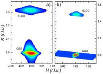
Figure 1. (a) RSM along H and K of a representative SLCO film grown on a GSO substrate around the symmetric (0 0 2) band asymmetric (1 0 3) Bragg reflections (panel (a) and (b), respectively). The units of H and K are those of the GSO pseudocubic reciprocal lattice.
Download figure:
Standard image High-resolution imageAt the same time, rocking curve measurements (ω-scan) have shown very close values of the full-width at half maximum for the SLCO films and the GSO (TSO) substrate, thus deducing that the film is commensurately strained to the underlying substrate. Such a fully-strained condition was also confirmed by asymmetric XRD measurements of the (1 0 3) Bragg reflection (panel (b) of figure 1). Figure 2 shows HAADF-STEM images of an x = 0.07 SLCO sample grown on TSO. The stark Z-contrast between the heavy Tb A-sites in the substrate and the lighter Sr and La in the film, confirms the atomically abrupt TSO/SLCO interface, the high structural quality of the sample and the fully strained growth of the SLCO film, which in this case has a thickness of about 30 nm.

Figure 2. HAADF-STEM image of a 30 nm x = 0.07 SLCO sample grown on TSO substrate.
Download figure:
Standard image High-resolution imageThe resistivity ρ of the samples has been estimated as:

where tSLCO is the film thickness obtained by the XRR analysis. We point out again, that, in the case of the electron doped IL compound, with only one CuO2 plane per unit cell, there is no ambiguity in identifying the truly conducting layer.
In figure 3, the room temperature normalized sheet resistivity ρ'/ versus the temperature T curves for the SLCO films with different doping are shown, where ρ' = ρ/c, with c the measured crystal axis along the growth direction (always around 0.34 nm), is (see equation (1)) the sheet resistance by the number of conducting planes. At high temperatures, the ρ'(T) curves of the under-doped and optimally doped samples (x ⩽ 0.1) show a linear behavior with no sign of saturation, starting from a doping dependent T* temperature, while the curves of the over-doped samples (x > 0.1, not shown here) present a tendency to saturation becoming more clear with increasing doping [26]. The room temperature values of the resistivity ρ273 of all the investigated samples were in the range 0.1–0.25 mΩ · cm (see table 1). For under-doped films, an upturn in the ρ' values before the superconductive transition is observed, becoming more evident with decreasing doping down to values where the superconducting transition is no longer present (not reported here). In table 1 we summarize the main structural and transport parameters for the investigated samples.
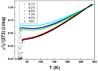
Figure 3. Room temperature normalized sheet resistivity versus the temperature curves for SLCO films with different doping.
Download figure:
Standard image High-resolution imageTable 1. Characteristic temperatures and resistivity values obtained for the investigated samples.
| x | Tc-onset (K) | Tmin (K) | ρres (mΩ · cm) | T* (K) | T** (K) | ρ273 (mΩ · cm) |
|---|---|---|---|---|---|---|
| 0.061 | 22 | 69 | 0.079 | 213 ± 3 | 203 ± 1 | 0.15 |
| 0.062 | 23 | 64 | 0.14 | 246 ± 4 | 215 ± 5 | 0.24 |
| 0.069 | 27 | 69 | 0.09 | 231 ± 2 | 191 ± 3 | 0.17 |
| 0.073 | 29 | 65.5 | 0.08 | 221 ± 1 | 170 ± 1 | 0.16 |
| 0.085 | 33 | No min | 0.05 | 194 ± 2 | 160 ± 5 | 0.13 |
| 0.1 | 35 | No min | 0.04 | 222 ± 1 | 163 ± 1 | 0.11 |
In the table 1, Tmin is defined as the temperature of the upturn (the local minimum in the ρ'(T) curves), the onset of the superconducting critical temperature Tc-onset is defined as the temperature at which ρ' is 90% of its value just before the transition starts (the local maximum for the under-doped samples with the upturn and the low temperature residual resistivity for the others) and T** is the highest temperature at which the ρ'(T) curves are well described by a T2 dependence. The data of Tc-onset, T* and T** in table 1, are also plot in figure 4. The red and black dashed lines are guides to the eyes. The T* and T** values associated to the optimally doped sample do not seem to follow the behaviour observed for the under doped samples. The sample with x = 0.061 has a low T* value probably due to its influence to extrinsic factors such as structural disorder or small stoichiometric inhomogeneity.

Figure 4. Plot of the Tc-onset, T* and T** data in table 1, as a function of the doping x. The red and black dashed lines are guides to the eyes.
Download figure:
Standard image High-resolution imageDiscussion
The low temperature upturn in the ρ(T) curves of under-doped cuprates has been related to several mechanisms such as Kondo scattering [6] or WL effects [7]. In SLCO films the presence of WL effects has been proven by low-frequency voltage spectral density measurements and it has been also proposed to influence the normal state transport properties in a larger temperature range [26]. Moreover, by suitably fitting the low temperature resistivity curves, the three-dimensional (3D) localization mechanism associated to the electron–phonon scattering was shown to give always a better agreement to the experimental data (in terms of the statistical χ2 test) when compared to the two-dimensional (2D) mechanism associated to a logarithmic correction, although the χ2 values related to the 3D and the 2D mechanisms had always the same order of magnitude (around 10−5) [26]. Here, to closely follow the work of Li et al [15] in order to compare our results to those obtained in [15], we have described the low temperature sheet resistivity curves using three terms

where  is the residual (T = 0) sheet resistivity, in general very close to the ρ'(Tmin) value and the Δρ'(T) term is associated to the low temperature upturn and has been phenomenologically taken, in agreement with the work of Li et al [15], to exhibit a logarithmic temperature dependence with Δρ'(T) = −Alog□log(T/Tlog). Posing A0□ =
  + Alog□log(Tlog/1 K), Li et al have fit their data by equation (3)

using A0□, Alog□ and A2□ as free fitting parameters. For both the hole and the electron doped cuprates, Li et al [15] have shown that the coefficient A2□ is independent of the particular type of material, shows similar values at the same level of n doping and is inversely proportional to the charge carrier concentration. They have also found A0□ ≈ x−3.4±−0.3 and Alog□ ≈ x−3.6±−0.3 doping dependencies with an approximately linear relationship between A0□ and Alog□ holding over many orders of magnitude. In table 2 we report the fitting results for the A0□, Alog□ and A2□ coefficients obtained for the investigated samples.
Table 2. Fitting parameters obtained for the investigated samples.
| x | A2□ (by equation (3)) (mΩ K−2) |  (by equation (4)) (mΩ K−2) (by equation (4)) (mΩ K−2) |
A0□ (Ω/u.c.) | Alog□ (Ω/u.c.) |
|---|---|---|---|---|
| 0.061 | 34.68 ± 0.09 | 28.74 ± 0.03 | 3591 ± 9 | 278 ± 2 |
| 0.062 | 46.8 ± 0.1 | 40.35 ± 0.03 | 5800 ± 9 | 341 ± 3 |
| 0.069 | 41.3 ± 0.1 | 33.35 ± 0.03 | 4226 ± 9 | 334 ± 3 |
| 0.073 | 42.94 ± 0.01 | 34.268 ± 0.009 | 3929 ± 9 | 345 ± 2 |
| 0.085 | 37.9 ± 0.1 | 36.47 ± 0.06 | 1497 ± 6 | 26 ± 2 |
| 0.1 | 33.09 ± 0.06 | 31.88 ± 0.03 | 1244 ± 6 | 25 ± 1 |
In figure 5, as an example to show the used fitting procedure, we report the ρ'(T) curve for the sample with x = 0.062 along with the fit to equation (3) (green dashed line) and the estimated contribution A0□ − Alog□log(T/1 K) (red dashed line).

Figure 5. Representative resistivity data for the sample with x = 0.062 showing the fitting procedure used to determine the parameters in table 2. The green dashed line is the fit to equation (3) and the red dashed line is the estimated A0□ − Alog□log(T/1 K) contribution.
Download figure:
Standard image High-resolution imageIn figure 6, are shown the A2□ values versus the doping x obtained by fitting with equation (3) the low temperature sheet resistivity curves of the samples in table 1.

Figure 6. A2□ values versus the doping x obtained by fitting with equation (3) the low temperature sheet resistivity curves of the samples in table 1. In the figure the  values obtained by equation (4) are also shown by magenta pentagons.
Download figure:
Standard image High-resolution imageThe red line in figure 6, is the 1/x dependence which is in reasonable agreement with data points Moreover, the A2□ values are very close to those obtained for other electron doped superconducting cuprate compounds at similar doping levels [15].
The A0□ values we have obtained by the same fitting procedure, are also dependent on the doping level, with A0□ ≈ x−3.6±0.1, which is the same exponent obtained by Li et al [15] for their n doped materials. The Alog□ values we have found for the samples with x < 0.085, are more scattered and do not show a clear relationship upon the doping (see table 2). However, we have found that a linear relationship among the A0□ and Alog□ values is still valid with data points approximately falling on the same curve followed by the data of Li et al [15].
The results of our analysis of the charge transport in SLCO films, with the A2□ coefficients showing 1/x dependence and values close to those observed in other electron doped superconducting cuprates at comparable doping levels, along with the similar x-scaling law of the A0□ coefficients, indicate the possible presence, in the low temperature range, of FL behaviors also in these IL electron doped cuprates. The scattered Alog□ values did not yield a clear doping relationship but do show a linear dependence with the A0□ values, as in the case of the other electron doped cuprates investigated by Li et al [15]. This could be probably traced back to the fact that, in the low temperature range Tmin < T < T**, the resistivity curves of the under-doped samples are very plausibly described in terms of the formula

where  is a constant. As a consequence, the difference between A0□ and Alog□, appearing in (3), is physically related to the constant value of the residual resistivity
  , resulting, therefore, in the linear dependence between A0□ and Alog□ values, independently of the particular doping. We have also fit our low temperature resistivity curves using equation (4). The
  values obtained by this procedure do not differ much from the A2□ given by the previous method and are shown as pentagons in figure 6. In the under-doped region the
  values are slightly higher than the A2□ ones, while, approaching the optimally doped regime, they start to coincide.
The results discussed so far, seem to confirm, in agreement to the work of Li et al [15], the presence of hidden FL charge transport in the low temperature properties of IL electron doped cuprate superconductors. To further analyze the normal state transport properties of our samples, we have also performed Hall measurements on typical under-doped samples (x ≈ 0.07). In figure 7(a)), it is shown the temperature behavior of  (T) = ρ'(T) − A0□ − Alog□log(T/1 K), figure 7(b)) presents 1/RH (where RH is the Hall coefficient) obtained after disentanglement of the logarithmic contribution [12, 15] from the resitivity ρ' and in figure 7(c)) the obtained temperature behavior for cot(θH) =
  / (HRH) is displayed. As it is clear from figure 7(c)), the cot(θH)(T) has a T2 dependence up to temperatures of about 120 K, close to the T** value and of the same order of the typical Neel temperatures observed in under-doped cuprates [2]. Differences between the temperature dependence of the Hall angle and the resistivity are not surprising, being the former more sensitive to changes in the Fermi surface than the latter, which is generally influenced also by other extrinsic factors. Moreover, the slope of the cot(θH)(T) curve in this temperature range (dashed red line in figure 7(c)) has a value of 0.0262, very close to the universal value found for other p and n doped superconducting cuprates [12, 15]. At higher temperatures the T2 dependence is lost and this is probably due to the presence of a more complex Fermi surface shape with the Hall coefficient ceasing to be a representative measure of the carrier density [27, 28].

Figure 7. (a) Temperature behaviour of  = ρ'(T) − A0□ − Alog□log(T/1 K), (b) temperature behavior of 1/RH, where RH is the Hall coefficient; (c) temperature behavior of cot(θH).
Download figure:
Standard image High-resolution image
Conclusions
We have deposited LaxSr1−xCuO2 epitaxial thin films on (1 1 0) GSO and TSO substrates by oxide MBE using a shuttered layer-by-layer deposition process performed in purified O3. XRD measurements indicated the preferential c-axis orientation of the films along the [0 0 1] substrate crystallographic direction without any sign of secondary phases and the presence of commensurate strain to the underlying substrate. The study of the normal state transport properties of our SLCO thin films, removing the ambiguity regarding the truly conducting layer, confirms the presence of a robust hidden FL charge transport in the low temperature properties of IL electron doped cuprate superconductors, in agreement with recent observations performed in other p and n doped cuprate materials, suggesting possible descriptions of the superconducting and normal state properties in these compounds independent of doping and carrier type.
Acknowledgments
B H Goodge and L F Kourkoutis acknowledge support from PARADIM, the National Science Foundation Platform for Accelerated Realization, Analysis and Discovery of Interface Materials under Cooperative Agreement No. DMR-1539918 and the Department of Defense Air Force Office of Scientific Research (No. FA 9550-16-1-0305). This work made use of the Cornell Center for Materials Research (CCMR) Shared Facilities, which are supported through the NSF MRSEC Program (No. DMR-1719875). The FEI Titan Themis 300 was acquired through No. NSF-MRI-1429155, with additional support from Cornell University, the Weill Institute, and the Kavli Institute at Cornell. The thin film growth work at Cornell was supported by the National Science Foundation (NSF) under Grant No. DMR-1610781.
Authors' contributions
Data curation: C Sacco, A Galdi, P Orgiani, N Coppola, H I Wei, L F Kourkoutis, K Shen. Investigation: C Sacco, A Galdi, P Orgiani, H I Wei, R Arpaia, F Lombardi, B Goodge, L F Kourkoutis, K Shen, L Maritato. Supervision: D G Shlom and L Maritato. Writing-orginal draft- C Sacco and L Maritato. Writing—review & editing-: C Sacco, N Coppola, A Galdi, P Orgiani, D G Schlom, L Maritato.