

Abstract
Interfacial phase change memory devices based on a distinct nanoscale structure called superlattice have been shown to outperform conventional phase-change devices. This improvement has been attributed to the hetero-interfaces, which play an important role for the superior device characteristics. However, the impact of grain boundaries (GBs), usually present in large amounts in a standard sputter-deposited superlattice film, on the device performance has not yet been investigated.
Therefore, in the present work, we investigate the structure and composition of superlattice films by high resolution x-ray diffraction (XRD) cross-linked with state-of-the art methods, such as correlative microscopy, i.e. a combination of high-resolution transmission electron microscopy and atom probe tomography to determine the structure and composition of GBs at the nanometer scale. Two types of GBs have been identified: high-angle grain boundaries (HAGBs) present in the upper part of a 340 nm-thick film and low-angle grain boundaries present in the first 40 nm of the bottom part of the film close to the substrate. We demonstrate that the strongest intermixing takes place at HAGBs, where heterogeneous nucleation of Ge2Sb2Te5 can be clearly determined. Yet, the Ge1Sb2Te4 phase could also be detected in the near vicinity of a low-angle grain boundary. Finally, a more realistic view of the intermixing phenomenon in Ge–Sb–Te based chalcogenide superlattices will be proposed. Moreover, we will discuss the implications of the presence of GBs on the bonding states and device performance.
Export citation and abstract BibTeX RIS
1. Introduction
As a new class of nano-engineered chalcogenide superlattices (CSL), interfacial phase change memory devices (iPCM) have gained much attention in recent years since they have been shown to outperform conventional phase-change devices in terms of switching speed, power consumption and cyclability [1]. The explanation for these improvements is still under debate. It may be an atomistic switching between two crystalline states or a process, similar to bulk PCM devices but enhanced by the nano-structuring itself [2, 3].
In an attempt to obtain an atomistic picture of iPCM structures, several studies pointed out that CSL structures of Sb2Te3 and GeTe show the tendency to intermix during deposition at elevated temperatures necessary for epitaxial growth [2, 4, 5]. For example, high resolution transmission electron microscopy (HRTEM) investigations revealed that the Ge atoms do not bind near the van-der-Waals (vdW) gaps but are rather intercalated in the adjacent Sb-layer of the Sb2Te3 quintuple layer (QL). Thus, locally a metastable phase of GeSbTe alloys is formed. Upon further ex situ annealing, these CSL structures gradually transform into a stable GeSbTe phase [5, 6].
Prior studies focused specifically on the stacking features within single grains of the CSL. However, no publications offer an undisputed overview of the role of grain boundaries (GBs). It is well known that epitaxially grown CSL layers are typically polycrystalline with grain sizes of several hundreds of nanometers. Thus a key question that we address in the present work is how the GBs impact the intermixing in iPCMs.
The standard characterization techniques, such as x-ray diffraction (XRD) or energy-dispersive x-ray (EDX) methods, used to investigate the CSL layers in iPCM, are able to determine e.g. the average structure and composition of the CSL film. Information about the local structure and chemical composition at individual GBs is not easily accessible. In the present work, the structure and composition of various GBs present in Ge–Sb–Te based CSL layers are investigated by applying electron back-scatter diffraction (EBSD), high-resolution (scanning) transmission electron microscopy (HR(S)TEM), and atom probe tomography (APT). The unique strength of APT techniques is to detect chemical inhomogeneities at the sub-nanometer level and in three dimensions [7, 8]. This is why phenomena, such as impurity segregation at interfaces and inter-diffusion between layers, can be easily discerned when applying APT [9]. Furthermore, APT can be easily combined with HRTEM providing a full comprehension of the structure and composition of the GBs at near-atomic level [10]. Moreover, we emphasize here that our study is focused on the GBs (character and composition; their impact on the intermixing) and not on the Ge and Sb diffusion mechanisms, since neither the present HRSTEM or APT studies are conclusive for understanding such mechanisms.
Thus, by applying APT and correlative APT-TEM we propose in the present work a nanoscopic scenario for the intermixing which takes place between Sb2Te3 and GeTe CSL layers. We will demonstrate indeed that the strongest intermixing between Sb2Te3 and GeTe CSL layers takes place at the high-angle GBs (HAGBs), where the heterogeneous nucleation of the metastable Ge2Sb2Te5 phase is proven for the first time. Classical intermixing between Sb2Te3 and GeTe CSL layers within single grains is also registered by APT, as proposed by various models in the field [8], leading to a maximum content of Ge in Sb2Te3 of ~15 at.%. This is indicative for the formation of a GeSb2Te4 metastable phase in agreement with our HRSTEM investigations.
2. Experimental Section
2.1. Sample preparation
GeTe and Sb2Te3 CSL with 20 repetitions has been sputter-deposited from stoichiometric targets of 4N purity on a Si(1 1 1) substrate with ρ > 5 mΩ cm at a deposition temperature of 200 °C. The DC power was 35 W with an Argon gas flux set to 35 sccm. The growth rate of GeTe and Sb2Te3 is 0.1 nm s−1. Superficial oxide on the substrate was removed beforehand by a wet-etch in aqueous hydrofluoric acid. The deposition was carried out at a base pressure of  10−8 mbar in a HV sputtering system with sputtering sources in confocal geometry and individually controlled shutters that allow precise control of the serial deposition.
2.2. Sample characterization
The electron backscatter diffraction (EBSD) technique was used to investigate the individual Sb2Te3 and GeTe layers. The EBSD system (AMETEK, NJ, USA) was integrated into the NanoLab system. The SEM was typically operated with an acceleration voltage of  and a beam current of
  , with a chamber pressure of about 10−6 mbar. The sample tilt and working distance were set to 70° and 13 mm, respectively. With these parameters, the EBSD lateral resolution was approximately 30 nm, and the typical exposure frame rates for the EBSD camera was around
  to 30 fps.
For the overall structural analysis, a Bruker D8 Discover setup equipped with a Goebel mirror, a Ge(2 2 0) asymmetric channel-cut monochromator and a Eulerian cradle was used.
The structural analysis at the atomic level was performed with an FEI Titan ChemiSTEM 80-300 Cs-STEM operating at 200 kV and equipped with a super-X detector. TEM lamellae were prepared with a focused ion beam (FIB) employing a FEI Dual Beam Helios NanoLab system and finally polished using a Fischione NanoMill at low energy (500 eV) to remove residual FIB-induced amorphization. Conventional TEM investigations for the correlative TEM-APT analysis were performed using a FEI Tecnai F20 microscope operated at 200kV.
APT measurements were carried out by CAMECA LEAP 4000X Si instrument with laser pulses of 355 nm wavelength (UV), 10 ps pulse length, and 20–25 pJ pulse energy. The specimen base temperature was set to 40 K. APT samples were prepared using FIB milling as described in [11]. To minimize beam damage, a low energy (5 keV) Ga beam was used at the final ion-milling stage.
3. Results
3.1. Structure of Sb2Te3–GeTe superlattices
The texture of individual 200 nm thick Sb2Te3 (R-3m crystal structure) and GeTe (R3m crystal structure) films sputter-deposited on Si(1 1 1) substrate was analyzed by EBSD. This technique provides the orientation of individual grains within the first 30-50 nm of the film. Hence, the character of the GBs can be directly determined.
Figure 1 shows that both films, Sb2Te3 and GeTe, contain predominantly red-colored grains, which correspond to the [0 0 0 1] (or [0 0 1]) growth direction as shown in (0 0 0 1) pole figures. This implies that Sb2Te3 and GeTe films have a common [0 0 0 1] (or [0 0 1]) texture. However, ~15% of grains in GeTe possess a second, less pronounced orientation, i.e. [0 −1 1 0] texture, colored on the inverse pole figure image in green (see figure 1(b)). For Sb2Te3 no other texture besides the [0 0 0 1] texture is detected. Yet, a considerable fraction of Sb2Te3 grains of approximatively 35% are randomly oriented in the film. Moreover, the averaged grain diameter in Sb2Te3 and GeTe thin-films has been determined to  µm and
  µm, respectively; in good agreement with the work of Saito et al [12] where the lateral grain size varied between 50 nm and a maximum of 300 nm.
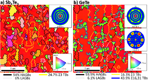
Figure 1. EBSD analysis of 200 nm thick individual Sb2Te3 and GeTe thin-films sputter deposited on a Si(1 1 1) substrate. The [0 0 0 1] or [0 0 1] texture is highlighted by red grains in both films. GeTe film possesses a second [1 0 −1 1] texture highlighted by green grains. 35% of grains in Sb2Te3 are randomly oriented. High-angle grain boundaries (HAGBs) are denoted by black lines, whereas low-angle grain boundaries (LAGBs) are highlighted by white lines. Moreover, Σ3 twin boundaries (TBs) are present in both films (yellow lines), whereas in GeTe additional types of TBs, i.e. Σ16 and Σ31, denoted by blue lines, are present in high proportion of 43.9%.
Download figure:
Standard image High-resolution imageFigure 1 also shows the identified GBs overlaid on a plot of image quality (IQ) for the Sb2Te3 and GeTe thin-films, respectively. Based on the misorientation (disorientation angle and plane orientation) several types of GBs are present, such as random HAGBs with disorientation angle larger than 15°, low-angle GBs (LAGBs) with disorientation angle smaller than 15°, and highly symmetric HAGBs called twin boundaries (TBs) with specific disorientation angles (for example the Σ3 TBs are characterized by a 60° disorientation angle). We note here that 60° angle does not correspond to a rotational symmetry, but to a defect, since in the trigonal and rock-salt structures there is only a 3-fold rotation symmetry (i.e. they can be rotated 120° each block of the stacking without producing a defect). In figure 1, the TBs are highlighted by yellow and blue lines, whereas the random HAGBs are highlighted by black lines. A high proportion of HAGBs ~94% and a low proportion of LAGBs ~6% were identified for both Sb2Te3 and GeTe thin-films. 24.7% and 16.3% of the identified HAGBs corresponds to Σ3 TBs in Sb2Te3 and GeTe, respectively. Additionally, the GeTe thin-film exhibits a high amount of Σ16 and Σ31 TBs with a fraction of 43.9%.
The structure of a ~330 nm thick [Sb2Te3–GeTe]20 CSL film (20 double-layers of Sb2Te3 and GeTe with trigonal space group symmetry P3m1) sputtered-deposited on a Si(1 1 1) substrate was investigated using XRD. The biaxial texture, observed with EBSD for the constituent materials was confirmed for the SL by means of a rotational  -scan of the
  peak family (see S1 in supplemental material available online at stacks.iop.org/JPhysCM/31/204002/mmedia). To analyze the stacking in growth-direction, figure 2(a) shows the results of an XRD
  symmetrical scan of the CSL sample.

Figure 2. XRD investigations of ~330 nm thick Sb2Te3–GeTe CSL layer sputtered-deposited on a Si(1 1 1) substrate. (a)  symmetrical XRD scan of the CSL film. The SL peak groups are highlighted in red. The peak positions of the mean lattice are indicated as red lines. The lattice determined for the supercell from the fit displayed in (c) is drawn in grey. Additional intensity (green) stems from the strongly scattering Sb2Te3 quintuple blocks. At these positions no individual satellite peaks are observed because of the superposition of coexisting supercells with different numbers of GeTe bilayers and/or GeSbTe insert layers. (b) Depicted is a detailed diagram of the first SL peak and its satellites shown in (a). The peaks were fitted with a set of pseudo-Voigt functions with equal distances and widths. The simulation of a perfect SL (grey) yields a supercell composed of 8.16 nm Sb2Te3 and 8.40 nm GeTe. (c) The linear fit of all observed SL satellites against the peak index yields a supercell size
  nm.
nm.
Download figure:
Standard image High-resolution imageThe two most intense diffraction features (at around  and
and  ) stem from the Si substrate. The three peak-groups, highlighted in red, are the so called SL peaks flanked by a number of SL satellites. The distance of the series of satellite peaks is known to be
  , where
  is the SL unit cell (supercell), i.e. one double-layer of Sb2Te3 and GeTe [13]. Hence, the supercell size is determined by fitting the satellite peak positions against a peak index (see figure 2(c)). To do that the peak groups are fitted with a set of superposed pseudo-Voigt functions of equal widths and distances (see figure 2(b)). With this the mean supercell size is determined to be
  nm.
nm.
The distance of the SL peaks (red lines in figure 2(a)) is related to the mean Te-sublattice throughout the CSL which encodes the average chemical composition [14] and yields  . Furthermore, we simulated the perfect superlattice structure using a kinematical scattering approach obtaining a best match in good agreement with the prior result with the XRD data for a CSL supercell of (8.16 nm Sb2Te3/8.40 nm GeTe). More details about XRD-spectra of CSL samples, fitting and stoichiometry determination can be found elsewhere [14].
Additional intensity is found at multiples of 
 (green highlight in figure 2(a)), which correspond to the strong scattering of the 8 quintuple blocks of Sb2Te3 within each supercell. There are broad peaks instead of individual satellite peaks observed, since supercells of slightly different sizes coexist in the CSL. The latter has been previously shown for samples grown by molecular beam epitaxy [5]. This understanding is further supported for the sputtered samples of this study by the TEM/APT analysis which shows defects, such as inserted GeTe bilayers and GeSbTe stackings, within the superlattice periods.
To determine the degree of preferential orientation (texture) of the grains in the film a rocking curve scan was performed (see figure S2 in supplementary information). The FWHM  indicates that [0 0 0 1] (or [0 0 1]) is the main growth direction (see figure S2) in agreement with the EBSD results obtained on individual Sb2Te3 and GeTe layers. However, the obtained value is larger than that obtained by other authors, but we note here that the deposited CSL layer is also thicker than the ones usually investigated (~340 nm, instead of ~50 nm). XRD probes the whole film, such that formation of defects predominantly in the upper parts of the layer will lead to an overall larger FWHM. This effect will be illuminated in the following local analysis by TEM and APT.
HRSTEM studies were also performed to investigate the structure of CSL layers at the atomic level. HAADF mode in STEM allows for direct interpretation of the micrograph intensity being roughly proportional to Z1.7 [15]. Along the zone axis investigated in the present work, CSL atomic columns are formed either by formal anions or cations. The formal anion columns are composed only by Te atoms while the formal cation ones are composed by Ge (in GeTe regions), by Sb (in Sb2Te3 regions) or by a mixture of Ge and Sb (in GeSb2Te4 or in Ge2Sb2Te5 regions). As Ge has a lower Z-value, i.e. intensity, than Sb and Te, darker spots in the micrograph correspond to Ge or to a mixture of the Ge/Sb while brighter spots correspond to Te, Sb, or a mixture of Sb and Te.
The STEM HAADF micrograph in figure S3 clearly shows the Sb2Te3–GeTe superlattice structure along the [1 1 –2 0] Sb2Te3 (or [1 –1 0]) zone axis. Sb2Te3 regions can be clearly distinguished by the higher Z-contrast and by the presence of 'vdW-like' gaps. The red box indicates the region in which a Z-contrast line profile was calculated. By means of the Z-contrast line profile we determined the thickness of the Sb2Te3 and GeTe regions in the micrographs. This provides only a rough estimation of the thickness because (i) the GeTe/Sb2Te3 interface is not always well defined and (ii) the procedure is possible only in the region in which the sample is exactly on axis, i.e. in a quite limited area. Nevertheless, we found the average thickness of Sb2Te3  and the average thickness of GeTe
  . The supercell size, estimated by HAADF, is therefore
  , which is in very good agreement with the XRD data. The larger error is due to the rough GeTe/Sb2Te3 interface that introduces an uncertainty of about 1 nm, i.e. one Sb2Te3 block.
In figure 3 we show HAADF STEM micrographs of the sample in cross-view (a) at low magnification, (b) medium magnification and (c) at high-resolution. The sample was tilted within the Si 〈1 1 0〉 zone axis so that the CSL layers are clearly visible. Figure 3(a) proves the typical polycrystalline structure of the sputter deposited CSL film. Diffraction patterns acquired at the bottom of the CSL layer (i.e. first 100 nm, see figure S4(b)) showed the presence of GBs with very low disorientation angles of maximum 5°, i.e. LAGBs, having almost no influence on the periodicity of the CSL. However, in the upper part of the CSL the GBs possess much larger disorientation angles >15° disturbing the periodicity of the superstructure strongly.
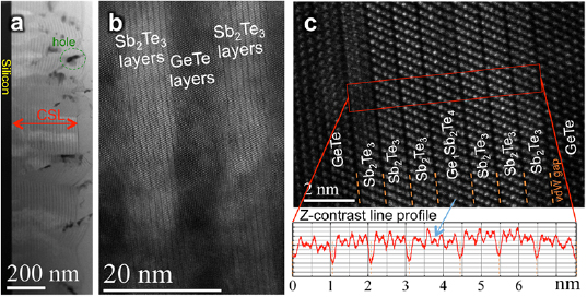
Figure 3. HAADF STEM micrographs of CSL layer sputter deposited on Si (1 1 1) substrate. The micrographs were acquired at (a) low magnification, (b) medium magnification, and (c) high-resolution. The sample was tilted within the Si 〈1 1 0〉 zone axis. Sb2Te3 regions can be clearly distinguished for the higher Z-contrast and for the presence of 'vdW-like' gaps ((b) and (c)). In (c) gaps are also marked with orange dashed lines. The red box indicates the region in which the Z-contrast line profile was calculated.
Download figure:
Standard image High-resolution imageIn figures 3(b) and (c), Sb2Te3 regions can be clearly distinguished by their higher Z-contrast and by the presence of gaps of lower intensity marked with orange dashed lines in figure 3(c). These are electron-depleted vacancy layers with a typically very low Z-contrast [16]. We note here that the distance between two Te atoms in these 'vdW-like' gaps (0.3 nm), is typically smaller than the real vdW-gaps, which is the distance between two graphene layers (0.335 nm [17]). Moreover, in figure 3(c) blocks of five layers about 1 nm thick are also clearly visible, typical of the Sb2Te3 stacking on the c-axis. Along the c-axis, the Sb2Te3 unit cell is given by the stacking of three blocks, i.e. 15 layers [6]. The red box in figure 3(c) indicates a region in which the Z-contrast line profile was calculated. In this line profile Sb2Te3 blocks appear to be well-divided by vdW-like gaps. However, we can also distinguish a block of seven layers, that is typical of GeSb2Te4. The presence of a low-Z element (Ge) was confirmed by the presence of a layer with a quite low intensity. Therefore, this observation clearly proves Ge diffusion into the Sb2Te3 layer. Moreover, in figure 3(b) (in the middle of the image where the sample thickness is constant) brighter regions are also present in the GeTe layer which suggests that Sb might have also diffused inside GeTe layer during the CSL deposition. Hence, the interdiffusion between the Sb2Te3 and GeTe layers explains why the Sb2Te3–GeTe interfaces are rather abrupt as clearly highlighted in figure 3(b).
Yet, these results are qualitative and not quantitative, i.e. we are unable to give an exact content of Ge in the Sb2Te3 layer. For this purpose, APT investigations have been performed inside CSL grains, but also at the GBs.
3.2. Composition of CSL grains at the nanoscale
Figure 4 summarizes a typical APT investigation of the entire CSL film with GeTe and Sb2Te3 layers repeated 20 times. The 3D reconstruction in figure 4(a) clearly shows an average layer thickness of ~8.5 nm for Sb2Te3 and ~7.5 nm for GeTe, in good agreement with the XRD and STEM experiments described before. We note here that the overall thickness of the CSL film (~340 nm) in the 3D reconstruction was calibrated based on the measured film thickness directly on the APT specimens by HRTEM. Figure 4(b) shows the 1D concentration profile constructed using a 30 × 30 × 0.2 nm3 sampling box placed perpendicular to the Sb2Te3/GeTe interfaces. Distinctive layers are clearly visible in the concentration profile. However, their composition deviates from the stoichiometric Sb2Te3 and GeTe composition.
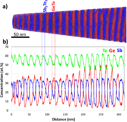
Figure 4. APT investigation of the entire CSL layer sputter deposited on Si (1 1 1) substrate. (a) 3D elemental map showing the redistribution of Sb (blue), Te (green), and Ge (red) in Sb2Te3–GeTe superlattices. (b) 1D concentration profile of Sb, Te, and Ge across the Sb2Te3–GeTe superlattices. Intermixing between GeTe and Sb2Te3 is clearly noticed by the presence of ~10 at.% Ge in Sb2Te3 and of ~15 at.% Sb in GeTe.
Download figure:
Standard image High-resolution imageThe APT experiments clearly show a chemical intermixing between Sb2Te3 and GeTe. First, a non-negligible amount of Ge is present in the Sb2Te3 layer, as expected from the STEM experiments. The content of Ge in the Sb2Te3 layers varies from one layer to another between 4 and 7 at.%. Second, surprisingly an even higher content of Sb is present in GeTe layer (5 to 13 at.%), information which was not accessible by STEM HAADF. For a broader overview, figure S5 shows the content of Sb in GeTe and of Ge in Sb2Te3 for three other APT measurements. We can clearly see that the maximum Ge (Sb) content in Sb2Te3 (GeTe) is 10 at.% (15 at.%). This suggests that the Sb is more soluble in GeTe than Ge in Sb2Te3 at temperatures of about 200 °C used during magnetron sputtering deposition.
3.3. Composition of the CSL GBs: correlative TEM-APT investigations
Correlative TEM-APT investigations were achieved directly on the APT specimens to understand the interplay between structure and composition at the nanoscale. Figures 5 and 6 show an example of such TEM-APT correlative investigations.
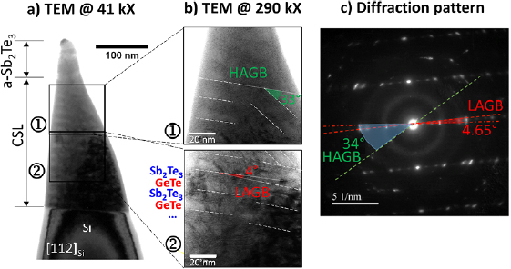
Figure 5. TEM investigations of the needle-shaped specimen. Bright field TEM micrographs were acquired at (a) 41 kX and (b) 290 kX magnification. At 290 kX magnification two GBs are clearly visible, i.e. a HAGB with a disorientation angle of 33° situated at the upper part of the needle-shaped specimen and a LAGB with 4° disorientation angle situated at the bottom part of the specimen. (c) Selecting area electron diffraction pattern acquired on the CSL film on a region of ~200 nm in diameter. This diffraction pattern confirms the presence of a HAGB and a LAGB in the needle-shaped sample.
Download figure:
Standard image High-resolution image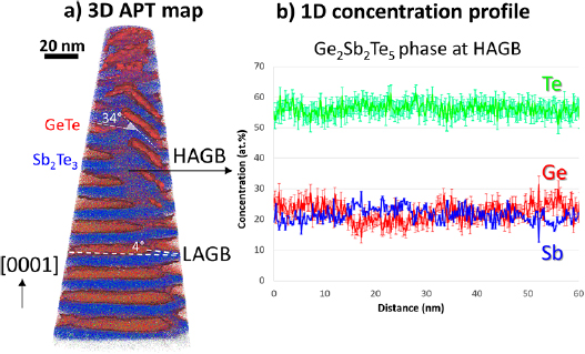
Figure 6. APT investigations of the needle-shaped specimen previously analyzed by TEM. (a) 3D elemental maps showing the redistribution of Sb (blue), Te (light green), and Ge (red) in Sb2Te3–GeTe superlattices. The GeTe layers are highlighted using an iso-concentration surface of 30 at.% Ge. (b) 1D concentration profile of Sb (blue), Te (light green), and Ge (red). This APT measurement reveals the heterogeneous nucleation of a Ge2Sb2Te5 phase at a HAGBs with a disorientation angle of 34°.
Download figure:
Standard image High-resolution imageThe needle-shaped specimen was first analyzed by TEM and the results obtained are summarized in figure 5. The bright-field TEM micrograph of the entire APT specimen acquired in low-magnification conditions (41 kX, figure 5(a)) exhibits a slight change in contrast between Sb2Te3 (darker contrast) and GeTe (brighter contrast) layers. By investigating the same APT specimen at higher magnification conditions of 290 kX, a HAGB and a LAGB are clearly visible in the upper and lower parts of the specimen, as highlighted in figure 5(b). We note here, that the disorientation angles of ~33° and ~4° were determined based on the Sb2Te3/GeTe interface orientation offsets registered in the APT specimen as highlighted by dotted-white lines. The presence of a HAGB and a LAGB inside the APT tip are further confirmed by the electron diffraction patterns acquired in the CSL layer using an aperture for selecting a sample area of 200 nm in diameter (diffraction pattern in figure 5(c)). The angles 34° and 4.65° obtained by this method match the previous values (there is only one crystallographic rotation of 180° for obtaining equivalent domains, and hence 0°, 4.65° and 34° correspond to 'rotational' defects). The diffraction pattern acquired at the CSL/Si interface (diffraction pattern in figure S4(a)) proves the  orientation relationship in line with XRD
  -scans (see figure S1 in supplementary material). Moreover, the first two CSL layers are slightly tilted by 1.5° with respect to the Si surface.
Finally, the same specimen was investigated by APT and the results obtained are summarized in figure 6. The Sb2Te3/GeTe interfaces in figure 6(a) are highlighted in the APT 3D reconstruction by an iso-concentration surface constructed using a Ge iso-concentration value of 30 at.%. These iso-surfaces confirm the presence of two GBs in the upper and lower part of the tip as highlighted in figure 6(a). Furthermore, the disorientation angle  could be determined directly on the 3D APT map by identifying the angle between the normal to Sb2Te3 (0 0 0 1) planes (i.e. [0 0 0 1] or [0 0 1] directions) of the neighboring grains as described in the supplementary material in figure S6(b). In contrast to TEM, where only the angle projected along the zone-axis can be determined, the angle obtained by APT can be precisely determined by taking into account the full 3D information on the detector. The disorientation angles for the HAGB and LAGB are
  and
and  , respectively, values in very good agreement with the TEM investigations presented in figure 5.
In the HAGB region a distinctive phase which corresponds to Ge2Sb2Te5 is identified. The 1D concentration profile from figure 6(b), constructed at the HAGB position using a sampling box of 13 × 7.5 × 6 nm3, clearly shows that the Ge, Sb, and Te average concentrations correspond to 22.3 ± 2.2 at.%, 21.5 ± 2.2 at.%, and 56 ± 2.6 at.%, respectively correspond to Ge2Sb2Te5 phase. Such a heterogeneous nucleation [18] of Ge2Sb2Te5 phase at the CSL GBs has not been reported before. This is mainly because of the very limited region where this Ge2Sb2Te5 phase is present (~8 nm wide and 60 nm long). Such information could not be obtained by STEM because the GBs, which are found in the ~50 nm thick TEM lamellae, are projected in 2D and, hence, such Ge2Sb2Te5 nanoprecipitates are impossible to detect. We mention here that we have observed the heterogeneous nucleation of the Ge2Sb2Te5 phase for other HAGBs investigated in the same sample. Thus we are describing a generic feature observed at HAGBs.
The question which may rise now is whether such a Ge2Sb2Te5 phase is also formed at LAGBs. Figure 7(a) depicts the 3D map of a small portion of a LAGB where (QLs are easily visible in Sb2Te3. These QLs are in general 0.8 ÷ 1 nm thick and contain approximately 4 at.% of Ge. However, there are particular regions close to the LAGB where layers thicker than 1 nm are present (see small sampling box situated in Sb2Te3 layer in figure 7(a) and the atomic density profile, i.e. the overall number of atoms detected per each bin of 0.1 nm, in figure 7(b)). Such layers are rather called blocks and are highlighted in figure 7(b) by a grey-colored region. The blocks B1 (~1.3 nm), B2 (~1.3 nm), and B3 (~1.5 nm) have a thickness larger than that of a typical 1 nm thick QL. Momand et al [6] determined, by direct HAADF STEM observations, the thickness of a Ge1Sb2Te4 block as typically 1.4 nm. This suggests indeed that the blocks B1, B2 and B3 correspond to Ge1Sb2Te4 phase (see table S1).
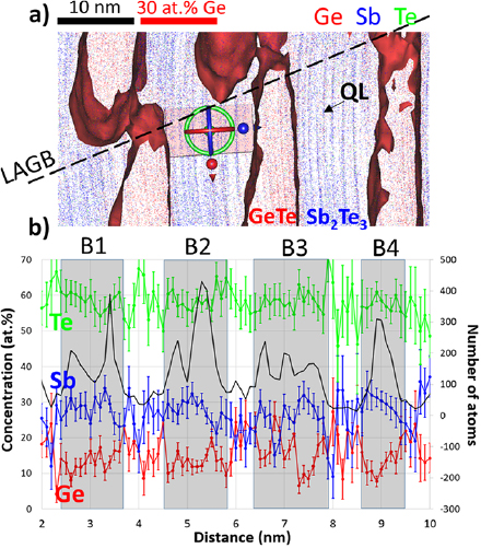
Figure 7. Cropped region highlighting the atomic redistribution near and at a LAGB. a) cropped 3D APT map from figure 6(a) highlighting the quintuple-layers (QLs) in Sb2Te3 and the shifted GeTe layers at the LAGB. The GeTe layers are highlighted using an iso-concentration surface of 30 at.% Ge. (b) 1D concentration profiles of Ge (red), Sb (blue), and Te (green) constructed within the pink box shown in a). The blocks B1, B2, and B3 have similar size and composition as the GeSb2Te4 phase, whereas the block B4 corresponds to the Sb2Te3 phase. The Ge concentration is even higher in the region between the blocks approaching the composition of the Ge2Sb2Te5 phase.
Download figure:
Standard image High-resolution imageThe detailed 3D composition measurements confirm the presence of both phases, Ge1Sb2Te4 and Ge2Sb2Te5, at the LAGB. Figure 7(b) summarizes the composition detected in each block and layer. The detected concentration values for Ge, Sb, and Te per each block are given in table 1. The compositions of B1, B2 and B3 (13.1 ± 2.6 at.% Ge, 27.8 ± 3.4 at.% Sb,) are indeed close to the composition of GeSb2Te4. We note here that we have identified the same GeSb2Te4 phase for other LAGBs investigated. However, the Ge concentration at the interfaces between these blocks which are only 0.5 ÷ 0.8 nm thick (such as B1/B2, B2/B3, and B3/B4; see table 1) was determined to be much higher approaching thus the composition of Ge2Sb2Te5. Although the width of these interfaces does not match with the c lattice constant of stable trigonal Ge2Sb2Te5 (1.7 nm) [6], the elemental composition corresponds to the Ge2Sb2Te5 compound.
Table 1. Summary of the Ge, Sb, Te concentration values inside and between each detected block (B). The composition of B1, B2, and B3 corresponds to the GeSb2Te4 phase, whereas the composition of the regions between the blocks (like for example B2/B3 highlighted in red in table) approaches the Ge2Sb2Te5 composition. The thickness of each block, but also the distance between each block is given.
| Element | B1 | B2 | B3 | B4 | B1/B2 | B2/B3 | B3/B4 |
|---|---|---|---|---|---|---|---|
| Ge (at.%) | 12.9 ± 2.8 | 13.4 ± 2.4 | 15 ± 2.8 | 12 ± 2.3 | 16.8 ± 4 | 20.8 ± 4 | 18.5 ± 7 |
| Sb (at.%) | 27.9 ± 3.8 | 27.8 ± 3.1 | 26.4 ± 3.5 | 29.7 ± 3.3 | 25.8 ± 5 | 21.6 ± 4 | 24.2 ± 7 |
| Te (at.%) | 59.1 ± 4 | 58.6 ± 3.5 | 58.4 ± 3.9 | 58.2 ± 3.5 | 57.3 ± 6 | 57.5 ± 5 | 57.2 ± 8 |
| Thickness (nm) | ~1.4 | ~1.4 | ~1.6 | ~1 | ~0.8 | ~0.5 | ~0.65 |
| Average (at.%) | Ge: 13.2 ± 2.5; Sb: 27.9 ± 3.3; Te: 58.6 ± 3.7 | Ge: 17.8 ± 4; Sb: 24.8 ± 5; Te: 57.1 ± 6 | |||||
| Total average (at.%) | Ge: 15.5 ± 4; Sb: 26.4 ± 4; Te: 7.9 ± 5 | ||||||
4. Discussion on intermixing at the nanoscale: role of GBs
Intermixing between Sb2Te3 and GeTe layers have already been observed for CSLs to occur during deposition by sputtering [10] or molecular beam epitaxy [10] mainly using HR(S)TEM. Wang et al [4] had proposed a novel growth model where pure GeTe layers are formed inside Sb2Te3 layer solely due to the intermixing at the interfaces between GeTe and Sb2Te3. Contrary to this idea, Momand et al [5, 6] argued that the formation of isolated and pure GeTe blocks in Sb2Te3 is not energetically favorable. Instead, they proved that a vdW heterostructure of Sb2Te3 and a stable GeSbTe phase forms upon intermixing of Sb2Te3 with GeTe. However, none of these studies have quantified the chemical changes in GeTe and Sb2Te3 layers upon intermixing at the nanoscale and in three-dimensions.
In the present study, we have demonstrated the capability to quantify chemical intermixing using APT. First the CSL grain composition was investigated. Surprisingly, beside the expected Ge content in Sb2Te3, an even higher Sb concentration of 5%–13% could be detected in GeTe layers. Pure GeTe layers inside Sb2Te3 were not observed, but Ge was rather found inside the QL and in-between QL at the vdW gaps. Second, the strongest intermixing was registered at the GBs, i.e. at HAGBs in the upper part of the layer where very high Ge concentrations were registered referring to the Ge2Sb2Te5 compound. On the contrary, at the LAGBs in the bottom part of the layer both GeSb2Te4 and Ge2Sb2Te5 nuclei were detected. Moreover, we verify the heterogeneous nucleation of Ge2Sb2Te5 compound at a HAGBs employing a novel correlative TEM-APT approach [10] backed by XRD structural data.
None of the existing intermixing models mentioned above [4–6] take into account the presence of GBs, where the intermixing process is supposed to be dramatically accelerated. Figure 8 summarizes a more realistic scenario for the intermixing process taking place in the CSL film, where the intermixing is observed not only inside the grains between individual layers, but also at the GBs positions. The random HAGBs (no symmetry relation between the neighboring grains) are highly disordered regions. Moreover, contrary to TBs, the energy of random HAGBs is relatively high mainly because of the atomic bonds which are strongly distorted or even broken [16]. The nucleation and growth of the metastable Ge2Sb2Te5 phase takes place most probably to minimize the free energy of HAGBs [19].

Figure 8. Schematic of the intermixing process between Sb2Te3 and GeTe layers at the bottom and upper part of the CSL layer.
Download figure:
Standard image High-resolution image
Ge2Sb2Te5 formed at such low temperature of ~200 °C is believed to be in a metastable form rather than the stable one. Nanoka et al [20] and later Matsunaga et al [21] have shown that the metastable Ge2Sb2Te5 phase with an NaCl-structure (Fm-3m) is formed upon annealing at 150 °C. The stable Ge2Sb2Te5 phase with a trigonal structure (P-3m1) is obtained only by annealing the sample at temperatures higher than 300 °C as shown by Bordas et al [22].
Two different APT observations confirm the metastable rock-salt structure of the Ge2Sb2Te5 phase. First, the APT 3D map does not show the presence of vdW-like gaps in Ge2Sb2Te5 as seen for Sb2Te3 ruling out the formation of a trigonal stable Ge2Sb2Te5 phase at the boundary. Second, our recent study showed that high probabilities of multiple events (more than a single ion detected per laser pulse) are observed by APT for 'metavalently bonded' materials [23] (called previously 'resonant bonding' materials [24]), contrary to covalent bonded materials where the registered probabilities for multiple events were rather low. In the present work, the registered multiple probability for Ge2Sb2Te5 phase is about 55%, which correspond rather to the rock-salt Ge2Sb2Te5 phase (58%) and not to the trigonal Ge2Sb2Te5 phase (63%, for details see [23]).
One needs to wonder what are the implications on the device functionality when the metastable rock-salt Ge2Sb2Te5 or Ge1Sb2Te4 phase are present at the GBs. Simpson et al [1] have demonstrated that low switching times (laser pulse duration of 25 ns) and currents (0.5 ÷ 1 mA) are necessary for iPCM to transit from the RESET (covalent) to SET (metavalent) state. These values are much lower than the typical values used for Ge2Se2Te5 devices (~100 ns, 1.5 mA). One may hence assume that the transitions between RESET (covalent) and SET (set) and vice-versa are not effectuated in the region of the GBs, and hence GBs are most probably regions non-operational in the iPCM cells.
Moreover, based on current study, the cycling performance of the iPCM may strongly decrease for layers thicker than 40 nm. Figure 8 clearly schematizes the formation of the HAGBs for layers thicker than 40 nm. As argued before, HAGBs act as a leakage channel in the device due to the formation of metastable Ge2Sb2Te5 phase, which was not previously predicted. The supposedly reduced cycling performance for films thicker than 40 nm has not yet been discussed in literature [1].
5. Conclusions
In the present work, the sputter-deposited Ge–Sb–Te based CSL have been investigated not only on the large scale obtaining precise information about the structure and crystal orientations with EBSD and XRD, but also locally using advanced nano-analytical techniques such as HR(S)TEM and APT.
By applying APT and correlative APT-TEM we propose here a novel scenario for the intermixing in Ge–Sb–Te based CSL. We demonstrate indeed that the strongest intermixing between Sb2Te3 and GeTe CSL layers takes place at the high-angle GBs, where the heterogeneous nucleation of the Ge2Sb2Te5 metastable phase is proven for the first time. Classical intermixing between Sb2Te3 and GeTe CSL layers within single grains is also registered by APT, as proposed by various models in the field, thereby finding evidence for the formation of GeSb2Te4 metastable phase.
Based on the multiple probabilities and structure registered at GBs, we concluded that a Ge2Sb2Te5 phase with metastable rock-salt structure has formed, for which much higher switching time and currents are necessary to switch between RESET (covalent) to SET (metavalent) states and vice versa compared to iPCMs. Thus, it is imperative to avoid the formation of such GBs region to maintain the advantages of iPCMs devices.
Acknowledgments
The financial support by the DFG through SFB 917 is gratefully acknowledged. The authors would like to thank Professor Joachim Mayer and Professor Rafal Dunin-Borkowski for their support by allowing the usage of the state-of-the-art TEM facilities available at RWTH Aachen and FZ Jülich.