

Abstract
In organic and hybrid photovoltaic devices, the asymmetry required for charge separation necessitates the use of a donor and an acceptor material, resulting in the formation of internal interfaces in the device active layer. While the core objective of these interfaces is to facilitate charge separation, bound states between electrons and holes may form across them, resulting in a loss mechanism that diminishes the performance of the solar cells. These interfacial transitions appear in organic systems as charge transfer (CT) states and as bound charge pairs (BCP) in hybrid systems. Despite being similar, the latter are far less investigated. Herein, we employ photothermal deflection spectroscopy and pump-push-probe experiments in order to determine the characteristics and dynamics of interfacial states in two model systems: an organic P3HT:PCBM and hybrid P3HT:ZnO photovoltaic layer. By controlling the area of the internal interface, we identify CT states between 1.4 eV and 1.8 eV in the organic bulk-heterojunction (BHJ) and BCP between 1.1 eV and 1.4 eV in the hybrid BHJ. The energetic distribution of these states suggests that they not only contribute to losses in photocurrent, but also significantly limit the possible maximum open circuit voltage obtainable from these devices.
Export citation and abstract BibTeX RIS
1. Introduction
Organic and hybrid photovoltaic devices continue to draw the attention of the scientific community due to their advantageous properties and potential for applications, e.g. inexpensive large-area fabrication. Despite remarkable recent advances in their power conversion efficiency [1–5], deeper understanding of the physical principles that govern the device function is required for further development. The active layers of these devices are prime examples for complex material systems, the function of which depends largely on the properties of their internal interfaces. Unlike traditional inorganic semiconductors, the process of charge separation in these systems requires the presence of energetic asymmetry, which is achieved by forming heterointerfaces between either organic or inorganic materials. Ubiquitously, the two material components of such a photovoltaic system are termed donor and acceptor, denoting the process of electron transfer from the former to the latter. Both organic and hybrid donor:acceptor interfaces exhibit rich photophysics that is of both fundamental and applied interest to the photovoltaic community. A key example of this, is the discovery and extensive investigation of the charge-transfer (CT) states at organic donor:acceptor interfaces [6–10]. Following a photoexcitation of the donor and the electron transfer to the acceptor, a bound CT state is formed between an electron in the lowest unoccuppied molecular orbital (LUMO) of the acceptor and a hole in the highest occupied molecular orbital (HOMO) of the donor [11, 12]. CT states have been observed in different material systems using different experimental techniques.
In general, the energetics of CT states can be probed using steady-state absorption and/or emission spectroscopy. The electronic wave functions of the donor and acceptor molecules are slightly mixed even prior to photoexcitation, leading to the formation of a weak ground-state CT complex [13–15]. For this reason, the transition from the ground-state to the exiplex state is partly allowed and a CT state can be formed directly upon photoexcitation. The measurements of absorption associated with transitions directly to the CT states are complicated by their low density and cross section. For many weakly interacting donor-acceptor combinations such measurements are not possible by traditional UV–visible (vis)–IR spectroscopy. Photothermal deflection spectroscopy (PDS) is a highly sensitive method to measure absorption that is based on the naturally occurring 'mirage effect' and is sometimes referred to as 'mirage spectroscopy' [16]. PDS uses the heat that is created by the dissipation of energy from the excited state to affect a change in the refractive index of a surrounding medium (typically an inert fluid). This change in refractive index will change the optical path of light passing through the heated region of the medium—the same effect that causes a mirage in a desert, or on a road on a hot day. This change can be detected by passing laser light through this region and monitoring the deflection of the output beam. As the laser beam intensity is constant, the impact of detector noise is greatly reduced. Using lock-in amplification (phase sensitive detection), further improves the accuracy of the PDS technique, increasing the measurement sensitivity by over three orders of magnitude as compared to conventional UV–vis–IR spectroscopy. In recent years, PDS has been succesfully utilized to investigate CT absorption in a number of organic material systems [14, 17–20]. Direct transitions from ground to CT states can also be observed by performing sub-bandgap external quantum efficiency measurements in which the yield of CT states is represented by the magnitude of photocurrent measured for excitations below the bandgap [21–23].
The dynamics of CT states can be probed using transient absorption spectroscopy, which uses the characteristic absorption features of neutral and charged excited states to resolve their evolution in time [24, 25]. Another ultrafast spectroscopy method developed specifically to address CT states is pump-push-photocurrent (PPP) spectroscopy. During a PPP experiment, the photoinduced formation of CT states (pump) is followed by providing additional energy to these states as an IR optical pulse (push). This push pulse releases charges from the bound CT states and thereby resulting in an increased photocurrent, which is detected using a lock-in amplifier [8].
The presence of CT states and their role as a loss mechanism in organic donor:acceptor systems was one of the motivating factors leading to the development of hybrid photovoltaics. In hybrid devices, the acceptor is replaced by an inorganic material, such as Si, Ge, ZnO or TiO2 [26]. It was generally considered that, since inorganic materials have significantly higher dielectric constants, charge transfer to these materials would immediately result in the formation of free charges that can contribute to the photocurrent. A variety of hybrid donor:acceptor systems has been explored in photovoltaic devices, however the performace of those systems was not dramatically improved compared to organic ones [27, 28]. Even hybrid dye-sensitised devices, that for years demostrated the highest performance among third-generation PVs, frequently suffered from imperfect harvesting of electrons from oxide interface, usually called 'injection' in this field [29]. In our previous work we applied PPP spectroscopy to hybrid solar cells based on the well-investigated poly(3-hexylthiophene-2,5-diyl):zinc oxide (P3HT:ZnO) system and have shown that photo-excitation results in the formation of bound charge pairs (BCP) at the hybrid interface, similar to CT states formed at organic:organic interfaces [30]. The yield of these BCP was ~50%, meaning that half of all excitons that reach the hybrid interface do not contribute to the photocurrent. This major loss mechanism explained why hybrid photovoltaic devices were so easily outperformed by organic-fullerene systems where charge separation is far more efficient [31]. Despite these results, a key advantage of the organic–inorganic hybrid system remains, which is the relative ease with which the hybrid heterointerface can be modified. For example, in the case of ZnO, surface modification can be easily achieved by depositing, for example, a phenyl-C61-butyric acid self-assembled monolayer. This modification resulted in a significant reduction of the yield of BCP (down to ~25%) and a significant enhancement in the photovoltaic performance [30, 32]. The improvement is not limited to an organic modifier, and similar enhancements in charge separation efficiency can be obtained with inorganic modifiers, for example a thin layer of caesium carbonate (Cs2CO3) [33]. An alternative method to modify the surface structure of the metal oxide is to introduce dopants into the layer during processing. Our first attempt was based on the introduction of Sr doping into the metal oxide, which resulted in an increased density of sub-bandgap states at the surface of the metal oxide. This was accompanied by an increase in the yield of BCP states and a reduced photovoltaic performance. This observation suggests that trap states at the surface of the metal oxide participate in the formation of BCP states [34]. To confirm this, we investigated another dopant, Cs+, the introduction of which resulted in a decrease in the density of sub-bandgap states. By gradually changing the doping level, we were able to correlate the yield of BCP states to the density of sub-bandgap states at the surface of the metal oxide. This confirmed that the formation of BCP states is directly linked to the trap density of the metal oxide surface [35]. Our current understanding of the charge separation process across a hybrid interface is based on electrons being trapped at surface trap states of the metal oxide. These trapped electrons then Coulombically attract polaronic holes on the polymer chains, resulting in the formation of BCP states.
Understanding the relation and resemblance between BCP and CT states is required for future improvements in hybrid photovoltaic devices. We aimed to energetically characterise CT states and BCP in common systems to investigate the similarity. While in the case of organic systems the spectral signature of CT states has been identified by PDS, very few such investigations have been performed for BCP states in hybrid systems. One rare example, was examined in P3HT:TiO2 via Fourier-transformed photocurrent spectroscopy. The interfacial transition was found to be in the systems bandgap between 1 eV and 2 eV [36]. For other systems no similar studies are available. The likely explanation for the lack of this information is the fact that both CT and BCP states scale with interfacial area and while it is relatively easy to fabricate organic bulk heterojunction (BHJ) stuctures with domains on the order of ~10 nm, it is far more complex in the hybrid case. Therefore ways to control the area of the internal interfaces were adapted and tested for both systems.
In this work, we apply PDS to an organic P3HT:fullerene and a hybrid P3HT:ZnO BHJ. We demonstrate that the CT band in the organic case can be easily identified by tuning the interfacial area between the donor and the acceptor. By synthesising P3HT and ZnO nano-particles and forming a BHJ with a large hybrid interfacial area, we are able to probe the BCP band absorption in a hybrid system. We complement these measurements with PPP spectroscopy studies that demonstrate that the observed band indeed originates from BCP absorption and is not related to morphology or doping effects. Finally, we compare the measured CT/BCP state energy to the measured open-circuit votlage of the corresponding devices and identify the energy loss in each system.
2. Experimental section
2.1. Sample preparation
For optical characterisation, the films were deposited on Spectrosils from UQG Optics. These substrates show very low absorption in the near IR regime, making them suited for PDS measurements. Solar cells were fabricated using pre-patterned indium tin oxide (ITO) substrates. The cleaning procedure was the same for all samples and involved five minutes in a sonication bath, first submerged in acetone and then in isopropanol. After blow drying, samples were kept for 10 min in an oxygen plasma at 0.4 mbar and 100 W.
2.1.1. Organic:organic sample preparation.
P3HT was purchased from 1-Material and phenyl-C61-butyric acid methyl ester (PCBM) from Solenne BV. The materials were dissolved in either toluene or chlorobenzene with concentrations of 30 mg ml−1. The fabrication of P3HT/PCBM bilayers with different grades of inter-diffusion was adapted from Treat et al [23]. In principle the inter-diffusion is achieved in the annealing process, utilising different temperatures. Bilayers and BHJ samples were put on pre-heated hot plates, which were set to the desired temperatures.
2.1.2. P3HT and ZnO nano-particle synthesis.
Organic and inorganic nano-particles (NP) were fabricated in two separate colloidal solutions. P3HT NP were synthesised through the injection of a 10 mg ml−1 solution of P3HT dissolved in chloroform into ethanol. The ratio was 1:2 and the mixture was ultra-sonicated with six 40 W and 20 s long pulses from a tip sonicator [37]. ZnO NP synthesis was performed using adapted procedures reported by Meulenkamp et al [38].
In order to spin-coat a BHJ of P3HT and ZnO nano-particles, the colloids were mixed. It was found that it is necessary to wash the ZnO NP in order to remove excess ions which destabilise the P3HT colloid. This was done following a recipe from Pacholski [39].
To obtain a bilayer sample, the particles were spin-coated one after the other. Whereas for a BHJ, the solutions were first tuned in concentration to shift the material volume ratio to 1:1, and subsequently mixed, and spin-coated on a Spectrosil.
2.2. Nano-particle characterisation
2.2.1. UV–visible (UVVis).
Transmission absorption measurement were performed on a JASCO V-670. Signals were baseline and background corrected to compensate for signals from the substrate.
2.2.2. Transmission electron microscopy (TEM).
The used microscope was a JEOL 2010 TEM. For sample preparation a suspended nano-particles were drop-cast on a TEM copper grid, which is covered by a layer of a supporting thin FormVar® film, topped with amorphous carbon. The characterisation was performed after complete solvent evaporation.
2.3. Photothermal deflection spectroscopy
The PDS setup was self-built and consists of two units: the tunable, pump light source and the probing station. The 150 W, white light of a xenon arc lamp from Ushio Inc. is spectrally split by an Oriel Instruments monochromator and chopped, before being focused into a fibre. The exit of the latter leads to the thin film sample, perpendicular to its surface. The, through light absorption, heated area is passed in close proximity by a red laser from Research Electro-Optics Inc., traveling parallel to the surface. It is deflected due to the change in the refractive index of the all surrounding liquid, Fluorinert FC-770 from 3M, which in turn is caused by the local heating. The deflection is measured by a position sensitive detector from Thorlabs and further analysed by a lock-in amplifier from Ametec. Its magnitude is proportional to the absorption of the sample [16]. The measured signal was scaled to a transmission absorption measurement for comparison.
Despite being designed for single layer measurements, it was possible to extract experimental data for bilayer samples. Through investigation on the influence on the different film architectures and theoretical estimation [40], it was concluded that the signals from the sub-bandgap regime correspond to changes in the energetic landscape rather than to new preconditions in the evaluation. In order to facilitate the adaption to the PDS signal, the intensity of the light passing through the films was measured in parallel and converted into UVVis data sets.
2.4. Solar cell fabrication
The base for either the organic or the hybrid structure was always the same. On top of pre-patterned ITO substrate a layer on ZnO sol–gel was spin-coated at 2000 rpm for 45 s. The recipe to prepare the ZnO solution was taken from Hofstetter et al [33]. The layer was annealed at 200 °C for 30 min.
For hybrid devices a P3HT layer was spin-coated on top using a 10 mg ml−1 solution. Afterwards 7 nm of MoO3 and 80 nm of Ag were evaporated. The devices were post-annealed at 140 °C for 10 min before being contacted and encapsulated.
The organic cells had the same enclosing layers, but instead of P3HT a BHJ of P3HT:PCBM was used. This layer was spin-coated at 1000 rpm for 60 s from a solution with a weight ratio of 1:0.8.
2.5. Solar cell characterisation
The photovoltaic parameters such as open-circuit voltage VOC, short-circuit current density JSC, fill factor and power conversion efficiency were determined using a Keithley 2450 Source Measure Unit to record the current–voltages characteristics. The necessary artificial spectrum 100 mW cm−2 AM1.5G was generated by a ABET Sun 3000 class AAA solar simulator.
2.6. Pump-push-photocurrent experiments
In pump-push photocurrent (PPP) experiments, two optical parametric amplifiers (TOPAS-Prime, Light Conversion) were seeded with 800 nm, ~35 fs pulses from a 4 kHz Ti:sapphire regenerative amplifier (Astrella, Coherent). To produce pump beams, either a 1200 nm signal output from one TOPAS was frequency-doubled in a β-barium borate crystal to generate the 600 nm light or a 1600–1900 nm idler output was doubled in the same crystal to generate 800–950 nm pulses. The 2000 nm idler output from the other TOPAS was used as the push, and modulated by an optical chopper at ~1.2 kHz. The devices under study were the same devices as those used for electrical characterisation. The pump and push were directed onto a ~0.3 mm2 spot on the devices. The push- and pump-induced photocurrent (dJ and J, respectively) were measured at their respective modulation frequencies (1.2 kHz and 4 kHz) by a lock-in amplifier working in current-detection mode (SR830, Stanford Research Systems). The delay between the pump and push pulses was controlled by delaying the pump with a mechanical delay stage with retroreflector.
3. Results and discussion
3.1. Observation of charge transfer transitions in an organic bulk heterojunction
To examine CT formation at internal interfaces of an organic photovoltaic system as a function of interfacial area, we fabricated bi-layers of P3HT/PCBM and employed the inter-diffusion method to gradually increase the interfacial area. Previously reported approaches to vary the interfacial area were based on either changing in the ratio of P3HT to PCBM [17] or the employment processing additives [18]. For example, the additives used by Buchaca-Domingo et al resulted in the expulsion of PCBM from the polymer crystallites, thereby changing the shared interface between the two components. In doing so, they were able to observe a transition in the bandgap which they correlated to CT states. Compared to this method, thermal inter-diffusion offers the advantage that possible contributions to the measured signals arising from the additives can be excluded. While an alternative method to vary the internal interfacial area without the use of additives is to vary the donor:acceptor ratio, the result is a variation in both the signals arising from the CT states as well as those from the material components, further complicating evaluation. Also this disadvantage is avoided by using inter-diffusion, as the relative amount of the materials is kept unchanged. To ensure no material degradation takes place, the inter-diffusion processing was limited in temperature range to below 200 °C. The principle of the interface area control is depicted in figure 1(a), with higher annealing temperatures resulting in larger interfacial areas [23].
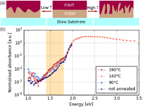
Figure 1. (a) Sketch to illustrate the control over the interface between P3HT and PCBM (b) Normalised absorbance measured via PDS for four P3HT:PCBM bilayers annelaed at different temperatures. Only for one exemplary curve also the bulk absorbance (2.0–3.5 eV) is shown. The CT state absorption (1.4–1.8 eV) is highlighted as an orange shaded area.
Download figure:
Standard image High-resolution imageFour samples with different interfacial areas (obtained upon annealing at four different temperatures) were probed by PDS. The results are shown in figure 1(b). For the visible light range no differences are detected. To facilitate the comparison in the sub-bandgap regime the curves were normalised to each other in the visible range. The normalisation additionally compensates for differences originating from slight variations in thickness of the measured films. In the range 1.3 eV to 1.8 eV an increase in absorption for increasing annealing temperatures can be noted. Taking into account the clear correlation with the expected interfacial area, we assign the observed absorption to the transition from ground state directly to the CT state. The energetic characteristics extracted from the data fit to previous reports of CT states in P3HT:PCBM [16]. It is intersting to note that the spectral distribution of the CT states does not change based on the interfacial area or typical domain size of each component, supporting the notion that CT states are local in nature.
3.2. Observation of BCP states in a hybrid bulk heterojunction
Having shown that the PDS is able to probe CT states related to large area internal interfaces in organic systems and knowing that such states also exist in hybrid systems, it is clear that in order to obtain information about their energetic characteristics it is necessary to fabricate a hybrid sample with a large interfacial area. Since inter-diffusion upon annealing a hybrid bi-layer is not a valid approach, the large interfacial area must be obtained by using nano-particles (NPs). Fabrication of hybrid ZnO NPs:polymer bulk heterojunctions can be easily performed by mixing in ZnO NPs into the polymer solution [41], but these often result in formation of NP agglomerates significantly limiting the interfacial area [42]. It is also possible to form ZnO directly within the P3HT film by either a conversion of diethylzinc into ZnO within the polymer film [43] or by atomic layer deposition [44, 45], however these methods do not allow simple fabrication of both a bilayer and a BHJ.
The approach chosen here is to synthesise colloids of both P3HT and ZnO NPs. These can be easily processed into both a bi-layer and a BHJ, thus offering control over the interfacial area. Previously reported routes were followed for the synthesis of the NP colloids (see experimental details for further information). The formation of nano-particles was confirmed via TEM and UVVis, as displayed in figure 2. The diameter of two types of nano-particles was found to be between 50 nm to 80 nm for P3HT and below 5 nm for ZnO (confirmed via dynamic light scattering (DLS), see figure S1 (stacks.iop.org/JPhysCM/31/124001/mmedia) in the Supplementary Information). P3HT nano-particles exhibit the same optical properties when compared to a spin-coated reference film, while a confinement effect which alters the optical band gap in ZnO nano-particles can be observed. For P3HT NPs, it is important to note that since their UVVis signal is identical to that of a spin-coated P3HT film (as well as emission, see supplementary information figure S2), the NPs consist of crystalline P3HT similar to the P3HT previously characterised as part of the organic system.
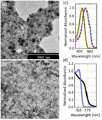
Figure 2. Left side, TEM pictures of (a) P3HT and (b) ZnO. Note the different scale bar, indicating the bigger P3HT nano-particles. Right side, UVVis spectra of (c) P3HT in solution (green), in film (blue) and as nano-particle film (red). (d) In black the spectrum of a non-nano-particle ZnO film and in blue the spectrum of a nano-particle film, showing a slightly increased bandgap.
Download figure:
Standard image High-resolution imageFigure 3 shows the results of the PDS measurements on hybrid bilayer P3HT/ZnO and bulk-heterojunction P3HT:ZnO systems. The curves are normalised to the maximal absorption peak in order to compensate for effects arising from different thicknesses. In the visible light range, the spectra appear similar. In the UV regime, the ZnO absoption edge can be identified. Due to the 1:1 volume ratio in the BHJ, the ZnO contributes stronger to the signal due to its higher abundancy when compared to the bilayer sample. The strong signal in the visible range originates from P3HT absorption and shows no differences for the two types of samples. However, changes are detectable below the band gap. A clear feature, corresponding to a near-IR excited transition, can be seen in the bulk heterojunction sample, but is not easily discerned in the bilayer one. The feature can be fitted using a gaussian distribution with an energetic position at 1.25 eV and a 2σ-interval of approximately 0.3 eV (see supplementary figure S3), which agrees to suggested values for this material system [30]. In a first instance, it is therefore associated to BCPs.
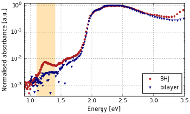
Figure 3. The results of PDS measurements of two samples with maximised (BHJ) and minimised (bilayer) internal interface were normalised at the peak absorption and depicted. The shaded area (1.1–1.4 eV) marks the most noticeable peak corresponding to BCP transitions.
Download figure:
Standard image High-resolution image3.3. Pump-push photocurrent spectroscopy on organic and hybrid BHJs
While the nature of sub-bandgap absorption in organic donor:acceptor blends has been a subject of intense discussion in the literature, the IR absorption in P3HT:ZnO can have different origins. One obvious possibility can be transitions involving defect states in the bulk and surface of ZnO. Another can be a transition between the ground state of P3HT and an interfacial charge electron-hole pair state similar to a CT state in organics. To identify the exact nature of the sub-bandgap absorption we have compared the photo physics of the materials after excitation of P3HT excitons and transitions in the near-IR. As the absorption is very weak, conventional pump-probe experiments are hardly possible for the studied systems as an increasing (weakly absorbed) pump intensity will lead to multiphoton artefacts in the experimental data. We therefore performed PPP experiments on actual working devices which can be done using very low excitation levels [46]. It is even sensitive enough to probe the dynamics of a bilayer P3HT/ZnO.
Figure 4 compares PPP data for organic BHJ and hybrid bilayer devices with P3HT and sub-bandgap excitation. In both materials, after P3HT excitation at 600 nm, we observe that a PPP signal associated with CT states and interfacial BCPs appears very early (immediately at our timescale) after excitation. The kinetics following excitation at 600 nm are somewhat different in the organic and hybrid devices, which is not surprising taking into account how different the acceptor material is. The decay time for organic devices were 150 ± 20 ps and decay times for hybrid devices were 250 ± 40 ps. However, importantly, for each material system the kinetics after excitation at 600 nm and in the near-IR are almost identical. This indicates that when sub-bandgap states are excited the photocurrent is generated through the same pathway—formation of interfacial charge pairs. This clearly rules out the possibility that the near-IR absorption in the hybrid system is associated to anything other than the BCP states formed at the P3HT/ZnO interface.
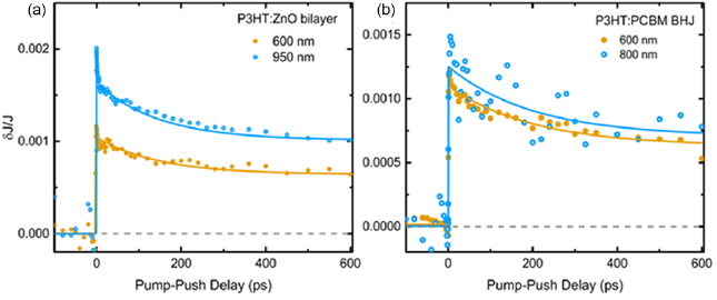
Figure 4. The results of PPP measurements for organic (a) and hybrid (b) photovoltaic diodes with direct excitation of the polymer at 600 nm and direct excitation of sub-bandgap states in the 800–950 nm region.
Download figure:
Standard image High-resolution image3.4. Comparison to open circuit voltage of photovoltaic devices
The characterisation of BCP and CT states allows us to draw similarities between the organic and hybrid system. First, our findings confirm that both hybrid and organic cells exhibit charges bound across the internal interface, perturbing efficient charge separation. Secondly, both types of states scale in their occurrence with the interfacial area between donor and acceptor. Additionally, both types of states lie energetically in the bandgap and show a similar dynamic under varying excitation wavelengths. Based on these similarities between the organic and hybrid cases, it is interesting to compare the energetic position of CT/BCP states with the open circuit voltage (VOC) of the corresponding photovoltaic devices (figure 5 and table 1). Upon a photoexcitation in the P3HT, charge transfer to the organic or inorganic acceptor may lead to the formation of a bound state. The energetic position of this state with respect to the ground state indicates the maximal accessible VOC. While the deviation between the maximum and measured VOC is large, both the organic and inorganic systems follow the same trend, i.e. the difference between the transition energy of BCP and CT states is in agreement with the difference in measured VOC (~0.3 eV) for each type of device. This further suggests that the interfacial states in both organic and hybrid systems affect the maximal available open-circuit voltage of the device in a similar fashion.

Figure 5. Schematic summary of the energetics in the different BHJs. The grey arrows mark the position of the interfacial states and simultaneously the maximal achievable open-circuit-voltage in such solar cells.
Download figure:
Standard image High-resolution image
Table 1. Comparison of energy differences of CT and BCP states and corresponding measured open-circuit voltages.
| Transition energy (eV) | Measured VOC (V) | |
|---|---|---|
| P3HT:PCBM | 1.4–1.8 | 0.62 |
| P3HT:ZnO | 1.1–1.4 | 0.37 |
| Offset in transition energy/change in VOC | 0.3 | 0.25 |
4. Conclusion
In this work we studied bound states of charges, which occur at internal interfaces of organic or hybrid solar cells. In order to identify these states, we varied the interfacial area of both types of systems and directly probed them by photothermal deflection spectroscopy. We characterised the spectral distribution of these interfacial states in an organic system and for the first time, also in a hybrid system. These distributions can be compared to the measured open circuit voltage of funtional devices and remarkably reveal that BCP and CT states impact the photovoltaic performance in a very similar fashion. This study highlights the potential of exploiting mitigation strategies already developed for suppressing the negative effects of CT states in organic solar cells and applying them to hybrid cells to further boost photovoltaic performances.
Acknowledgments
AAB is a Royal Society University Research Fellow. The authors would like to kindly thank Professor U Bunz for providing access to device fabrication and film characterisation facilities. We also thank Y Sevinchan for initial optimisation of the P3HT nano-particle synthesis routes. ZC, HX and YV acknowledge the PROCES project (ANR-17-CE05-0028-01 and DFG 391347809). DB-K and YV thank the DFG for financial support (SFB 1249, project C4).