

Abstract
Electronic structure calculations for a homo-material semimetal (thick Sn)/semiconductor (thin Sn) heterodimensional junction and two conventional metal (Ag or Pt)/silicon hetero-material junctions are performed. Charge distributions and local density of states are examined to compare the physics of junctions formed by quantum confinement in a homo-material, heterodimensional semimetal junction with that of conventional Schottky hetero-material junctions. Relative contributions to the Schottky barrier heights are described in terms of the interface dipoles arising due to charge transfer at the interface and the effects of metal induced gap states extending into the semiconducting regions. Although the importance of these physical mechanisms vary for the three junctions, a single framework describing the junction energetics captures the behaviors of both the heterodimensional semimetal junction and the more conventional metal/semiconductor junctions.
Export citation and abstract BibTeX RIS
1. Introduction
Semimetals are considered as semiconductors having a either a 'zero' or 'negative' energy band gap. This leads to a metallic character near the Fermi energy but there is a low density of states (DoS). The nature of the semimetal band structure near the Fermi energy combined with quantum confinement in low-dimensional semimetals leads to a semimetal-to-semiconductor transition. The transition arises when the confinement length becomes comparable to the Fermi wavelength of the electrons and/or holes [1]. This leads to semimetal electronic behaviour being observed for three-dimensional (3D) or bulk samples, whereas semiconducting behaviour emerges for samples that are patterned as two-dimensional (2D) films or one-dimensional nanowires. This property of semimetals allows for a novel means for making rectifying junctions within a single material. Formation of a hetero-dimensional (3D–2D) rectifier in a bismuth film consisting of a thicker semimetallic region abutting a thinner 2D region, with a thickness much smaller than the critical length for the semimetal-to-semiconductor transition and thus displaying semiconducting behavior, has recently been experimentally demonstrated [2, 3] at room temperature.
To explore the properties of heterodimensional Schottky-like junctions formed in a single material and relying on quantum confinement, first principle calculations are applied to compare the semimetal junctions to more conventional metal/semiconductor Schottky junctions. In this way, we highlight the similarity of a monomaterial Schottky barrier formed between a 3D-to-2D junction to the more conventional approach of forming a heterojunction between a metal and semiconductor. As pointed out in [2–4], the use of a semimetal avoids the need to form a heterojunction or to introduce doping in a homojunction to achieve a current rectifier or diode. This approach thus offers advantages in the fabrication of novel electronic devices on the length scale of a few nanometer. To construct a Schottky barrier transistor, two metallic regions are required to define source and drain regions that are separated by a semiconducting channel. With the correct selection of metals and semiconductors, the source–channel and channel–drain junctions result in the formation of Schottky barriers. Similarly, the same effect can be achieved in a semimetal thin film or nanowire by narrowing a central region to form a semiconducting channel between larger, semimetallic source and drain regions [2–4].
This study explores the electronic structure at a Schottky barrier junction formed by at a 1 nm thick 2D film of α-tin (α-Sn) abutting a 3D electrode also consisting of α-Sn. Although α-Sn is not stable at room temperature in bulk form, it has been experimentally demonstrated that a stable α-Sn phase can be achieved in thin films [5–8] including for critical thicknesses whereby the film remains semimetallic or the induced band gap energy is small enough such that charge carriers can be thermally excited into the conduction band at room temperature. The energy band gap of the thinner region is controlled by varying the film thickness or cross-sectional area of the semimetal nanowire [1–4, 9] and a film thickness of 1 nm is chosen in this study to yield a band gap of the order of 0.5 eV which is sufficient to form a Schottky diode capable of operating at room temperature. This prototype of a monomaterial Schottky junction form by an α-Sn semimetal (thick)/semiconductor (thin) interface is compared with two conventional metal/silicon (Pt or Ag)/Si Schottky junctions.
The simplest approach to understanding metal/semiconductor junctions is the Schottky–Mott rule which provides an estimate of the resulting potential barrier height based on the metal's work function and the semiconductor's electron affinity. In practice though, the rule does not prove to be a reliable predictor of the Schottky barrier height as it ignores surface chemistry and particularly charge transfer at the interface leading the formation of an interfacial dipole. Metal-induced-gap states (MIGS) at a Schottky junction can also shift the band alignments near the interface or pin the bands in the semiconducting region to an energy level independent of the metal's work function. To investigate these effects for monomaterial semimetal junctions, explicit electronic structure calculations are undertaken to determine and compare the magnitude of the charge transfer at the interface for the three junctions described above, and to understand the similarities and differences between the semimetal and conventional Schottky barrier properties.
2. Methods
The electronic structure of the Schottky junction formation is determined based on density functional theory (DFT). The DFT Hamiltonian is used to determine electrode self-energies to describe 'semi-infinite' electrodes achieved by periodic extension of the 3D semimetal/metal and the 2D semiconducting regions at distances far from the junctions as implemented in the Atomistix ToolKit [10, 11]. An explicit device region encompassing the junction region is then treated by adding the energy-dependent complex self-energies to the device region Hamiltonian. Including the self-energies explicitly opens the system by application of the boundary conditions suitable for the NEGF boundary conditions using the self-energies calculated for semi-infinite electrodes. In directions parallel to the interface, periodic boundary conditions are applied leading to a 3D region abutting a 2D thin film. The explicit junction is shown in figure 1 for each of the three simulation cells studied and in each case the cell size is chosen to be sufficiently large to eliminate coupling between the electrodes as required to apply standard NEGF boundary conditions. A much longer semiconducting region relative to the semimetal/metal region due to the much larger screening lengths for semiconductors relative to metals is required to ensure that the junction electrostatics does not influence the charge neutral boundary conditions. The use of the semi-infinite electrode boundary conditions is in contrast to applying periodic boundary conditions in the direction normal to the junction interface which can lead to spurious interactions between periodic images. The NEGF boundary conditions enable isolation of a single junction with electrodes at equilibrium to provide an accurate description of the charge transfer processes for completely isolated junctions. The semimetal/metallic 3D regions to the back of figure 1 with the semiconducting slabs to the fore.

Figure 1. Atomic structure of (a) monomaterial junction, and (b) the metal/Si junctions. The metallic region is at the back of the figure. The lateral directions are periodic creating a 3D–2D junction. The non-equilibrium Green's function (NEGF) electrodes are created through self-energies that mathematically extended the 3D semimetal or metallic regions and the 2D semiconducting regions forming semi-infinite regions extending from either side of the interface. Two metal gates are shown in the figure adjacent to the junctions above and below the semiconducting region within the simulation cell and are used to examine the effect of electrostatic gating on the potential barrier formed at the interface between the two regions.
Download figure:
Standard image High-resolution imageThe simulation cell for the α-Sn junction has a cross sectional area parallel to the junction of 0.459 × 5.057 nm2, the periodic boundary conditions parallel to the junction lead to the smaller length given the repeat unit in the plane of the thin film region and the larger length refers to the repeat unit normal to the film. The length normal to the junction is 56.82 nm and is chosen to ensure that the device regions on either side of the junction exceeds the electrostatic screening lengths the ensure the effects of the charge transfer at the junction do not have an effect at the boundary conditions at the edge of the cells described by the self-energies for neutral electrodes. The explicit simulation cell for the junction consists of a total of 1532 Sn atoms. The cell dimensions lead to a repeat unit consisting of an 88 atom α-Sn cell for the bulk (3D) electrode and a 28 α-Sn atoms terminated by 8 hydrogen atoms per repeat unit for the thin film (2D) electrode used in the determination of the electrode self-energies.
The two metal-Si junctions have a cross sectional area of 0.38 × 4.59 nm2, again the shorter length refers to the repeat unit in the film and the longer length refers to the cell dimension normal to the film. The device region length is 56.51 nm, similarly larger than the electrostatic screening lengths in both material regions so that the electrode boundary conditions may be applied. Within the explicit device region, there are 288 metal atoms and the silicon thin film region consists of 1396 silicon atoms. For the metal–Si junction electrodes, a 96 metal atom repeat unit and 24 Si atoms terminated by 12 hydrogen atoms per repeat unit are used to calculate the respective self-energies.
All electronic structure computations are performed with the framework of DFT. The local-density approximation (LDA) is used for the exchange–correlation (XC) potential [12] when determining the relaxed junction atomic configurations. All structural relaxation is performed with the maximum force of less than 0.02 eV Å−1 on all unconstrained atoms. The Kohn–Sham orbitals used to determine the total electronic density have been expanded using a linear combination of double-ζ numerical atomic orbitals including polarization functions [10]. The energy cut-off has been set to 180 Rydberg. The magnitude of the band gap is a key physical quantity in understanding the band offset and potential barrier at Schottky junctions, but common XC functionals used in DFT calculations typically underestimate the band gap energies leading to an overestimate of electronegativity. This in turn leads to an overestimate of charge transfer at metal/semiconductor junctions. To improve the electronic structure description for the relaxed DFT/LDA junction geometries, a better estimate of the band gap energies is made using a meta-generalized gradient approximation (meta-GGA) XC functional. If properly calibrated, meta-GGA has been demonstrated to provide band gap energies comparable to experimental values for many semiconductors as demonstrated in the original formulation of the method [13]. The improvement is achieved at the cost of the introduction of an empirical parameter c which is selected self-consistently.
The semimetal simulation cell leads to a 2D α-Sn film with (1 0 0) surfaces and of 1 nm thickness abutting a bulk α-Sn electrode as shown in figure 1(a) chosen to model a semimetal heterodimensional junction. For α-Sn, the bulk electronic structure is described as having a zero band gap with the conduction and valence bands meeting at the Fermi level. Following calibration of the meta-GGA functional to improve the electronic structure description of the semimetal junction, calculations for the band structure for thin α-Sn films are used as a calibration value with the GW approximation to provide a description of the quantum confinement effects [14]. An empirical parameter c in the meta-GGA functional is selected such that the resulting energy band gap matches that calculated using the GW approximation and the final value obtained is c = 1.045 for the α-Sn calculations. Note this procedure results in the correct zero band gap for bulk α-Sn suggesting the meta-GGA approximation provides an improved description for the bulk and 2D electronic structure of the α-Sn junction particularly near the Fermi level of the equilibrated junction. Consequently there is a significant improvement in estimates for the band alignments between the two regions particularly for energies near the band edges in comparison to commonly applied approximations to the XC functional in DFT such as LDA or GGA. Charge equilibration requires the work function of the semimetallic region to align mid gap of the intrinsic semiconducting region. In this case, the band offset for the semimetal junction is approximately half the magnitude of the induced band gap in the quantum confined semiconducting region, if neglecting band bending near the junction.
The metal/semiconductor junctions are constructed using either silver (Ag) or platinum (Pt) 3D contacts abutting a silicon thin film with surface orientation of (1 0 0) and of 1 nm thickness as shown in figure 1(b). Ag has a lower work function than Pt, therefore the choice of these two metals allows for a comparison of a semimetal junction to conventional Schottky junctions of with differing barrier electronegativities. The crystallographic orientation of the metal regions is selected to keep the system size computationally tractable by minimizing the strain at the interface and to be compatible with the constraint of having a small number of metal atoms per simulation supercell. It is assumed that the metal electrodes are more malleable in terms of atomic rearrangements relative to the stronger covalent bonding occurring on the silicon side. Hence the lattice constant mismatch is chosen is chosen by relaxing the silicon slab and applying the resulting lattice constant to the explicit simulation cell. To relax the metal/Si junctions, the 16 Si atomic layers nearest the junction are allowed to relax whereas the silicon atoms furthest away from the junction are constrained to the relaxed geometry obtained for the silicon slab [15]. For the resulting metal/Si interfaces, the interfacial Si dangling bonds become located above hollow sites of the Ag and Pt atoms (1 0 0) surfaces. For the metal/Si junctions, the meta-GGA fitting parameter value of c = 1.088 that reproduces the bulk Si band gap is used for the Si thin film and leads to predictions of a band gap in the silicon thin film that is comparable to those obtained using the empirical pseudopotential method [16]4.
3. Results and discussion
The energy-resolved local DoS (LDoS) across the junctions are plotted in figures 2(a)–(c) obtained with both electrodes held at the same voltage or equivalently with the junction at equilibrium. As seen from the LDoS in figure 2(a) for the monomaterial α-Sn junction, the conduction and valence bands bend slightly upwards near the junction. At distances greater than approximately 20 nm into the semiconducting region, the semimetal work function aligns approximately to mid gap of the quantum confinement induced band gap of the thin film region. This alignment is consistent with charge transfer being localized to the vicinity of the junction and reflects that the simulation cells are sufficiently large to correctly treat electrostatic screening effects. In contrast in figures 2(b) and (c), it is seen that the band bendings at the junctions for the metal/silicon junctions are downward in energy and that as for the semimetal junction, the metal work function aligns approximately to mid gap of the silicon thin film band gap at large distances into the semiconducting region. The band bending measured in the conduction bands are +0.18 eV, −0.25 eV, and −0.22 eV for the thick/thin α-Sn, Ag/Si and Pt/Si junctions, respectively. Averaging the Hartree potential over lengths larger than the distance between atoms in the junctions results in a smoothing of the atomic scale oscillations in the electrostatic potential profile [10, 14]. The resulting averaged Hartree potential is shown by a yellow dashed line in the LDoS plots in figures 2(a)–(c). The electrostatic potentials displays a similar behavior as the conduction LDoS near the junctions. Similar plots of the LDoS under application of positive and negative gate voltages are shown in figure 3.
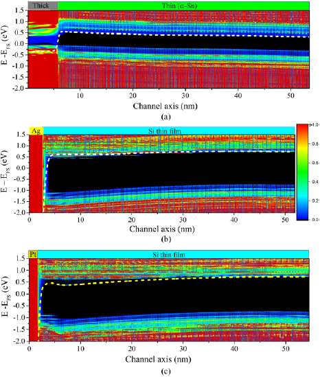
Figure 2. Equilibrium local density of states (LDoS) at (a) thick/thin α-Sn, (b) Ag/Si, and (c) Pt/Si junctions shown as a function of position normal to the junction. The zero of energy is taken to be the chemical potential of the equilibrated junction. The dashed lines show the macroscopic Hartree potential averaged over planes normal to the junction.
Download figure:
Standard image High-resolution image
Figure 3. LDoS of (a) thick/thin α-Sn, (b) Ag/Si, and (c) Pt/Si junctions under +1 V (left column) and −1 V (right column) gate bias. The application of the gate voltage reduces and increases the junction barrier height for positive and negative biases, respectively. The color legend is the same as given in figure 2.
Download figure:
Standard image High-resolution imageThe Schottky–Mott rule proposes that the potential barrier between a metal and semimetal can be given as the difference between the work function of the metal and the electron affinity of the semiconducting region

which assumes the vacuum level aligns across the junction or equivalently that there is no charge transfer across the junction. In equation (1),  is the Schottky–Mott estimate,
  is the metal work function, and
  is the semiconductor's electron affinity. The Schottky–Mott rule is known not to accurately predict measured Schottky barrier heights [17]. An improvement to the model is obtained by considering deviations from bulk charge distributions for the constituent materials to be localized near the junction interface leading to a correction to the Schottky–Mott rule given by

The change due to chemical bonding across the junction leads to charge transfer that can in a first approximation be treated as a surface dipole with a corresponding interface potential given by  . Motivation for applying equation (2) is obtained when examining the surface charge distributions for the monomaterial α-Sn junction, the Ag/Si junction, and the Pt/Si junctions represented in figure 4 as planar averaged charge difference densities (CDD). The CDDs are obtained as the difference between the total valence charge density and a superposition of neutral atom valence charge densities at each atomic site. In order to estimate the dipole at the junctions, the macroscopic average of the CDD has been extracted and compared at equilibrium (no bias across the Schottky barrier) and at equilibrium with different gate biases for the semimetal/semiconductor (thick/thin) α-Sn and metal/semiconductor (Ag/Si and Pt/Si) junctions as shown in figures 2 and 3 for the LDoS and in figure 4 for the charge densities. The magnitudes of the dipole peaks are calculated by an averaging of the CDD and this procedure can vary with the width of the Gaussian kernels used to define a macroscopic average [10, 14]. Hence, to have a consistent comparison of the dipole magnitudes, the same distance either side of each sampling grid point is considered in the macroscopic averaging scheme used for each of the three junctions. In all three cases, significant charge redistribution occurs at the interfacial bonds and the charge transfer leading to the formation of the surface dipole is from semimetallic or metallic regions to the intrinsic semiconductor regions.

Figure 4. Planar average of the CDD for (a) semimetal/semiconductor (thick/thin) α-Sn, (b) Ag/Si, and (c) Pt/Si junctions for applied gate voltages of −1 V, 0 V, and +1 V. Insets show details of the CDD at the interfaces and with the vertical dashed lines indicate the metallurgical junction location.
Download figure:
Standard image High-resolution imageThe equivalent planar charge density for the interface-induced dipole charges is calculated by integrating the CDD from the metallurgical junction to a distance of 8 Å into the metal and 8 Å into the semiconducting regions. Surface charge densities of 1.5 × 10⁻³ e Å−2, 5.86 × 10⁻³ e Å−2, and 1.44 × 10⁻² e Å−2 are obtained for the thick/thin α-Sn, Ag/Si, and Pt/Si interfaces, respectively. Using a parallel plate capacitance approximation with the integrated charge densities and the distance between the charge maxima taken as the spacing between the capacitor plates, estimates of the potential energy difference across the junction capacitors is found to be 0.14 V, 0.54 V, and 1.29 V for the thick/thin α-Sn, Ag/Si, and Pt/Si junctions, respectively.
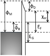
The charge distributions at the junctions suggest that a surface dipole or interface gap model for the interface potential can be used in equation (2) to estimate barrier heights. This idea is re-enforced by the LDoS resolved by atomic layer shown for the Ag/Si junction in figure 5 whereby a strong metallic character is seen only for the silicon atoms bonding directly to Ag atoms. In table 1, the energies required to describe the three junctions are given. Values are extracted from the LDoS for the equilibrium junctions as presented in figure 2. The smaller difference between the work function of the semimetallic region and electron affinity for the quantum confined semiconducting region for the α-Sn junction results in a relatively small surface dipole and hence a relatively smaller correction to the Schottky–Mott rule. There is a larger difference between the work function for the Ag electrode and the electron affinity for the silicon slab, consequently the charge transfer for the Ag/Si junction is larger than for the semimetal junction. Finally, the largest Schottky–Mott barrier difference is between the work function for the Pt electrode and electron affinity of the Si slab leading to the largest interfacial dipole of the three junctions. A simple model of the energetics of the junctions is shown in figure 6 in which the work function of the electrode is required to align to mid gap of the intrinsic semiconducting regions, and whereby it is assumed that the charge transfer required to equilibrate the junctions is restricted to be within a few atomic layers about the interface between the metallic and semiconducting regions. The last condition implies little or no band bending can occur at the junction.
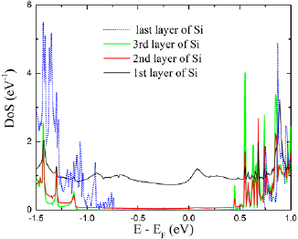
Figure 5. Projected DoS onto Si layers at the Ag/Si junction, where the 1st layer denotes the plane of silicon atoms nearest the interface and subsequent layers are relative to the junction. Note that the charge transfer to the silicon atoms is to a large degree localized directly at the junction interface.
Download figure:
Standard image High-resolution imageTable 1. Values for the metal electrode work function ϕM, the Fermi level (electrochemical potential) EF and the electron affinity χsc in the semiconducting electrode, the estimate for the interface potential from the parallel plate capacitor approximation qVcap, the dipole potential ϕD from the interface gap model shown in figure 6, the Schottky–Mott estimate ϕS-M for the Schottky barrier, and the Schottky barrier  from the interface gap model with no band bending or equivalently half of the energy band gap in the semiconducting region EG/2 (see figure 6), and the Schottky barrier height ϕB including band bending at the junction. All values in electron volts (eV).
| Junction | ϕM | EF | χsc | qVcap | ϕD | ϕS-M |  |
ϕB |
|---|---|---|---|---|---|---|---|---|
| Thick/thin α-Sn | 4.27 | 4.14 | 3.86 | 0.14 | 0.28 | 0.41 | 0.28 | 0.46 |
| Ag/Si | 4.71 | 4.20 | 3.47 | 0.54 | 0.53 | 1.24 | 0.74 | 0.49 |
| Pt/Si | 6.02 | 4.20 | 3.47 | 1.29 | 1.83 | 2.55 | 0.74 | 0.52 |
Figure 6. Energies of a Schottky junction in the approximation where the interface potential  describes the electrostatic potential of a surface dipole arising from interfacial bonding and charge redistributions required to align the metal region's work function and the semiconductor region's electrochemical potential (Fermi level). The Fermi level lies at mid gap in the thin α-Sn and Si films reflecting that they are intrinsic semiconductors. In this approximation, the Schottky barrier height
  becomes EG/2 where EG is the band gap. The band gaps obtained for the thin α-Sn and Si films including quantum confinement effects are 0.57 eV and 1.47 eV, respectively. Additional quantities are listed in table 1.
Download figure:
Standard image High-resolution image
The main focus of this study is dopant-free structures, however, as an example the LDoS across the junction for an n-type Si film with doping concentration of 1019 cm−3 is presented in the online supplementary material (stacks.iop.org/JPhysCM/30/414003/mmedia) showing the upward band bending as anticipated for charge transfer to the metal region from the semiconducting region. The band bending for the n-type Schottky barrier alignment results in charge carriers being transferred to the metal region with the charge being balanced at the junction by ionized immobile dopant cations in the semiconductor region. This mechanism is absent for intrinsic junction semiconductors but nonetheless there are charge transfer effects beyond that described solely by the interface dipole. Near the valence band edges for the intrinsic semiconductor regions shown in figure 2, there are MIGS as seen in the LDoS in the semiconducting regions. The valence band edge in figure 2(a) of the α-Sn semiconducting region in the vicinity of the semimetal junction aligns closely to the work function level in the α-Sn semimetallic region with accompanying MIGS extending up to 40 nm into the α-Sn semiconducting region. The MIGS provide additional charge transfer at the junction beyond the description provided by the assumption that the semiconducting bands remain flat as depicted in figure 6. The upward band bending seen for the valence band is also observed for the conduction band edge as well as in the electrostatic potential profile. The DoS associated with the MIGS is low but their spatial extent is relatively large. Although the resulting band bending is relatively small, it is of the same order of magnitude as the band offset given by the required surface dipole potential to achieve charge equilbration which predicts a barrier  = 0.28 eB as given in table 1. The increase in the Schottky barrier after including band bending ϕB = 0.46 eV is also included in table 1 for comparison.
In contrast, the overall charge transfer in the Ag/Si and Pt/Si junctions results in and overall downward bending in the Si band edges in the vicinity of the Schottky barrier. The downward band bending indicates a lowering of the conduction band offset with respect to the interface gap model; values of  and ϕB for these junctions are likewise listed in table 1. The much larger difference in the metal work function ϕM and the semiconductor electron affinity χsc for the Pt/Si junction compared to the Ag/Si junction requires a larger dipole potential correction ϕD to achieve equilibration. Nonetheless, the interface gap model predicts for both junctions a Schottky barrier height
  = EG/2 with EG the band gap in the silicon thin film. The similar magnitude of the band bending at the two junctions maintains approximately equal Schottky barrier heights ϕB. Given the large work function difference between Pt and Ag, this result cannot be anticipated by the Schottky–Mott rule. The estimate for the junction potential energy from the surface dipole treated as a parallel plate capacitor are given in table 1 as qVcap. For the Ag/Si junction, the parallel plate voltage qVcap is approximately equal to the dipole correction ϕD required to equilibrate the junction. There is a much larger difference between the values of qVcap and ϕD for the Pt/Si junction. This implies for the Ag/Si junction, the interface capacitance provides a good estimate of the charge transfer to form the Schottky barrier, whereas for the Pt/Si additional charge transfer mechanisms are present. Comparing figures 2(b) and (c), additional MIGS are seen near the Si valence band edge at the Pt/Si junction relative to the Ag/Si junction. The additional MIGS lead to additional charging in the vicinity of the interface not captured in the surface dipole contribution. However, the additional charges from the MIGS adds to qVcap providing the potential difference required to align the metal work function and semiconductor chemical potential. The net result is the simple model prediction of equal barrier heights remains the same, but reduced due to the band bending not include in the model of figure 6.
4. Conclusions
An atomic scale perspective of Schottky barriers for heterodimensional semimetal/semiconductor (thick/thin) and metal/semiconductor junctions is provide and related to simple models of Schottky junction physics. Through DFT calculations using a meta-GGA approximation to the exchange correlation potential, details of the electronic structure of the junctions is explored. To ensure that a single junction in isolation is studied, boundary conditions from the NEGF approach are used treating semi-infinite electrodes with the use of self-energies.
The electronic charge distributions across the junctions are obtained, and as well the energy band alignments and Schottky barrier heights are extracted from the energy resolved local density of states. The Schottky–Mott rule is introduced and correlated to the charge transfer. Although not a reliable predictor for barrier heights, the Schottky–Mott rule is a good indicator for the relative charge transfer at the junction. Analysis of the charge transfer reveals the spatial extent and magnitude of the surface dipoles arising between the metallic/semimetallic and semiconducting regions. The surface dipole potential is approximated by a parallel plate capacitance and compared to the correction in the Schottky–Mott rule required to align the metal/semimetal region's work function to mid gap at large distances into the semiconductor region. The interface capacitor potential is a good approximation to the correction to the Schottky–Mott rule for the Ag/Si junction, but underestimates the correction required for the α-Sn thick/thin junction and the Pt/Si junction. Additional effects due to MIGS and the surface dipole potential at distances away from the junction play a role and result in band bending corrections for all three junctions; the results are summarized in table 1. The combined effects lead to a strong p-type alignment for the α-Sn thick/thin junction and n-type alignments for metal/Si junctions. Although the work function difference between Pt and Ag is large, the overall physics of the two metal/Si junctions conspire to produce approximately equal Schottky barrier heights, the strong p-type alignment results in a similar conduction band barrier in comparison to the Ag/Si and Pt/Si junctions but essentially no barrier at the valence band for the α-Sn thick/thin junction. There is a significant dependence of the Schottky barrier height on the interfacial chemistry that drives the charge transfer across the junction. The charge transfer produces an interfacial dipole creating an electric field across the junction. Thus the Schottky–Mott rule cannot provide an accurate value for the potential barrier height. When the charge transfer at the interface is known, the Schottky–Mott rule can be modified by a surface dipole correction to provide an improved estimate of the barrier height [17], but additional electrostatic effects can be of the same order of magnitude as the correction term.
The semimetal thick/thin or heterodimensional Schottky junction is seen to behave similarly to conventional metal/semiconductor junctions. The physics of the junction formation is subject to the same considerations as for metal/semiconductor junctions. The behaviour of the barriers due to external gating is similar for the three junctions. In the absence of MIGS, the junctions are well described by the interface gap model which does not require the introduction of Fermi level pinning but relies on near ideal bonding at the interface. In these cases or when there is a small density of interfacial states, the potential barrier at the junction can be 'collapsed' due to shifting of the electrochemical potential in the semiconducting region [18]. The possibility of making semimetal heterodimensional junctions with uniform chemical bonding at the interface promises the possibility of fabricating ideal Schottky barriers closely mirroring the behavior of the ideal junctions described within the calculations presented.
Footnotes
- 4
Zunger et al [8] therein.