

Abstract
We investigate the atomic structure of Sn dimer chains grown on the Si(1 0 0) surface using non-contact atomic force microscopy (NC-AFM) at cryogenic temperatures. We find that similar to the native Si(1 0 0) dimer structure, the ground state of the Sn dimer structure is buckled at low temperature. At 5 K we show that the buckling state of the Sn dimers may be controllably, and reversibly, manipulated with atomic precision by close approach of the tip, without modification of the underlying substrate buckling structure. At intermediate cryogenic temperatures we observe changes in the configuration of the dimer chains in the region where the tip-sample interaction is very weak, suggesting that the energy barrier to transit between configurations is sufficiently small to be surmounted at 78 K.
Export citation and abstract BibTeX RIS
1. Introduction
The study of the self-assembly of 1D nanostructures on the Si(1 0 0) surface [1–3] has been motivated in part because of the attractive proposition of being able to form wires of single atom width without the need for direct photolithographic patterning. This work has, for the most part, been motivated by the significant interest in miniaturisation in the semiconductor industry, and therefore had a strong focus on the electronic properties of low dimensional structures on the atomic scale. These 1D structures also serve as a fascinating set of prototypical systems for investigating single atom processes at the atomic scale, and for testing the accuracy of ab initio simulations [4–6].
Although semiconductors are usually more stable than metallic systems, the reconstructions of some semiconductor surfaces nonetheless present a fascinating experimental and theoretical challenge due to the bistable configuration of the atoms at the surface. Indeed, as has been discussed extensively elsewhere, the Si(1 0 0) [7] surface offered a unique challenge in that the dimers that make up the surface are known to be bistable at room temperature, resulting in an apparent symmetric phase [7–9]. This bistability means that the surface is also extremely sensitive to perturbation by the investigating probe [10, 11]. Therefore interpretation of imaging of the surface has required significant theoretical input [12], and must be interpreted with explicit consideration of both the surface temperature [8], and the imaging mechanism [13–15].
Because the absorption of other group XIV elements at room temperature results in self assembled structures that mirror the structure of the silicon surface itself, the investigation of these structures presents similar challenges to those encountered when looking at the clean surface. Although the structures have been extensively investigated at the atomic scale both experimentally by use of STM [2, 3, 5], and computationally by ab initio calculation [4–6], a key limitation is the intrinsic convolution between the electronic and topographic properties of the chains that results from the nature of scannng tunnelling microscope (STM) imaging [6]. Although it is known that several types of metal dimer chain should possess a buckled ground state [2, 16], as with investigations of the silicon dimers there remains some debate as to how this buckling should be affected by the local surface structure.
These atomically defined structures are ideal candidates for single atom manipulation experiments, which are generally concerned with the ultimate 'digital' control over matter, and have been an active area of research since the pioneering work by Eigler et al [17]. While manipulation experiments using STM have undoubtedly demonstrated extreme levels of control over the positioning of single atoms and molecules [18–20] many forms of manipulation utilise the application of high electric fields, or the injection of tunnelling electrons, to induce excitation of the target atom or molecule. Although this limits their application to metallic, or highly doped semiconductor, substrates, the power of the technique in the engineering of functional atomic scale devices has been clearly demonstrated by the fabrication of single atom transistors and atomically thin wires on passivated semiconductor surfaces [21, 22].
An alternative manipulation strategy involves the direct application of mechano-chemical force to the targeted atoms or molecules via close approach of the scanning probe tip. This mode can be utilised in STM experiments, but the close approach of the tip can result in high current densities at finite sample bias, which introduces the potential for perturbation via current induced excitation. Operation at zero bias can help separate the contribution of the mechanical and current based effects [23] but requires the experiment be performed 'blind' as with no current there is no experimental observable during conventional STM operation. Conversely, use of force-based techniques such as non-contact atomic force microscopy (NC-AFM), which image via measurement of force, rather than tunnel current, allow for routine atomic resolution imaging and manipulation at zero bias. Since NC-AFM utilises the measurement of the change in resonant frequency of an oscillating cantilever to detect the interaction between the tip and surface [24], it in principle offers certain advantages over STM, as it is primarily sensitive to the atomic scale topography, and chemical reactivity [25], rather than the convolution of electronic structure and topography intrinsic to STM measurement. Most fundamentally, its mode of operation allows for the possibility of operation on insulating substrates, and measurement of the force during manipulation procedures. These experiments allow valuable insight into the processes that occur during manipulation via mechano-chemical processes [26, 27]. Because the forces are highly localised in the tip-sample junction, force-based manipulation has the potential to be more spatially precise than current-based manipulation techniques, which can in turn be important in situations where the system is particularly sensitive to external perturbation [10, 12, 28, 29].
From a fundamental science perspective, semiconductor systems offer important advantages with regards to developments in single atom manipulation, as the energy barriers involved in these systems are significantly higher than those typically encountered on metal, or ionic crystal surfaces. Consequently, it has been shown that use of semiconductors permits control of matter on the single atom level even at room temperature, allowing access to processes that were previously restricted to cryogenic temperatures. These have included lateral [26], and vertical [27] single atom manipulation via mechano-chemical means, and resolving the intramolecular structure of single molecules [30]. Thus far, however, there have been a very limited number of atomic resolution studies of metal chain structures [31, 32]. Nonetheless, these studies clearly demonstrate the potential for NC-AFM in identifying the atomic structure, and chemical make-up of the chains, as compared to the data obtained in the STM channel in the same studies.
In this paper, we use NC-AFM to investigate Sn dimer chains on Si(1 0 0) at 5 K. Due to the high resolution offered by this technique, and the stability afforded by low temperature operation, we are able to unambiguously confirm the buckled ground state of the dimers that make up the self assembled chains. Furthermore, via close approach of the scanning probe tip, we are able to controllably manipulate this buckling state using mechano-chemical force [11]. We also show how modification of the scanning parameters can result in an apparent symmetric dimer configuration, similar to the transition observed during imaging of the Si(1 0 0) surface itself [10, 29]. Finally, data acquired at an intermediate temperature suggests that the dimers in the chains are structurally unstable even at 78 K. We compare and contrast these results to previous room temperature and low temperature STM studies of similar systems, and ab initio calculation of the energy barriers associated with the structures.
2. Experimental details
We used a commercial low temperature (LT) STM/NC-AFM instrument (Scienta Omicron) operating in UHV cooled to either 5 K (LHe) or 78 K (LN2). Clean Si(1 0 0) surfaces were prepared by standard flash annealing of arsenic doped silicon wafers to 1150 °C, and then slow cooling from 900 °C to room temperature. A low coverage of Sn was prepared by exposing the room temperature silicon wafer to a molybdenum crucible containing high purity Sn (Goodfellow Cambridge Ltd.) heated by electron bombardment, for approximately 3 min.
Commercial qPlus [33] sensors (Scienta Omicron) with electrochemically etched tungsten wire tips, were used, and introduced into the scan head without any ex situ tip treatment. The tips were prepared on the silicon surface by standard STM methods (voltage pulses, controlled contacts with the sample) before performing NC-AFM experiments, and consequently we assume our tips are (bulk) silicon terminated.
Site-specific tip-sample forces were measured by performing  spectroscopy on the feature of interest, and over the bare substrate, subtracting one from the other (i.e. extraction of site-specific interactions [34, 35]) and subsequent inversion to force by the Sader-Jarvis algorithm [36]. As noted previously [11], the assumption that the off curves only contain long range force contributions is not strictly valid as we are able to observe weak site-specific interaction with the surface (i.e. atomic contrast) in constant height imaging due to the relatively long range extent of the silicon dangling bonds of the exposed surface. As a result, all forces presented here should slightly underestimate the true tip-sample interaction, but we believe this systematic underestimation to be preferable to the greater uncertainties that would be introduced by attempting a long-range fit of the van de Waals and electrostatic background [37, 38].
In this manuscript all NC-AFM images were acquired in true constant height mode, or in the adaptive height mode recently introduced by Moreno et al [39]. Therefore the images presented in the figures are  f maps. These are plotted in greyscale where darker features represent a more negative
  f and brighter features represent more positive
  f values. In our analysis we presume that more negative
  f values correspond to an increased attractive interaction between the tip and sample, and more positive
  f values represent less attractive (or repulsive) interactions. Some care must be taken with this assignment as rigourously the assignment of the sign of the
  f to the direction of the force can in general only be performed after inversion of a complete
  curve to force, as variation in the shape of the tip-sample potential, and the size of the oscillation amplitude, can result in even qualitative changes in the evolution in
  f constrast [40]. When performing experiments at 78 K, or acquiring grids of data over long periods of time at 5 K, we used a custom-built atom tracking system [41, 42] to correct residual thermal drift and piezoelectric creep. In all NC-AFM imaging we maintained a Vgap of approximately 0 V, such that no tunnel current was detected.
3. Surface overview
Because the manipulation protocols described later in the paper utilise particular intrinsic properties of the Si(1 0 0) surface and grown Sn chains, it is worth reviewing some of the key features of both structures. The native Si(1 0 0) surface is now recognised to form rows of alternately buckled silicon dimers, with each dimer having a topographically higher ('up') and lower ('down') atom. The ordering of the dimers in consecutive rows of the surface has two possible configurations, with in-phase and out-of-phase buckling in the rows offering the possibility of a p( ) and c(
 ) reconstruction respectively (figure 1(a)). Importantly, the barrier for dimers to change configuration (i.e. so called 'flip-flop' motion) is easily surmounted by the available thermal energy at room temperature. This very rapid motion results in an time-averaged apparent p(
 ) phase at room temperature.
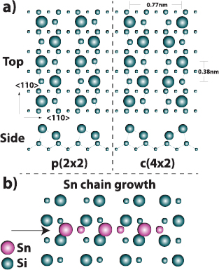
Figure 1. (a) Ball and stick model of the Si(1 0 0) surface showing the p( ) and c(
 ) reconstructions that arise from differences in the buckling orientation. The scaling of the top-most layer has been exaggerated to highlight the difference in the up and down atoms of the dimers. The upper diagram shows a top down view, the lower diagram shows an end on view looking down the rows. (b) Ball and stick model showing the orientation of the Sn chain growth on the Si(1 0 0) surface, the same exaggerated scaling between the up and down atoms has been applied.
Download figure:
Standard image High-resolution imageIt has previously been shown that the silicon dimers can be manipulated at low temperature, both by injection of tunnelling electrons [15, 28], and also by direct chemical interaction with the scanning probe tip [10, 11]. In the latter case, this manipulation is understood to occur when a chemical bond forms between the lower atom of the dimer and the terminating atom of the scanning probe tip for the case of reactive (e.g. silicon- or tungsten-terminated) probes. The formation of this bond 'pulls' the lower atom of the dimer up into contact with the probe, with a resultant 'toggling' of the buckling state of the dimer.
As noted above, deposition of metal adatoms onto the Si(1 0 0) surface results in the growth of 1D chains for many different elements. Although more sophisticated structures exist [32], most of these chains are formed of dimers of the deposited material running perpendicular to the direction of the dimers rows of the silicon surface (figure 1(b)). Depending on the material, these dimers are either symmetric, or buckled, like the silicon dimers [31]. In this paper we only consider the case of Sn dimers, which are thought to have a buckled configuration, and discuss their manipulation via an analogous mechanism to that described for the native silicon dimers.
4. Results
4.1. STM and NC-AFM imaging
Figure 2(a) shows a large scale STM overview of the Si(1 0 0) surface after deposition of a low coverage of Sn. The contrast we observe is broadly in line with previous studies of the same system performed at room temperature [2]—we observe small chains of dimers growing perpendicular to the direction of the silicon dimer rows, in addition to a number of isolated dimer units oriented both perpendicular and parallel to the dimer rows. Figure 2(b) shows a high resolution scan showing a chain of three, chain of two, and single dimer units. The positioning of these structures is in line with previous studies [2], confirming that the dimers in the chains sit above the trenches between the rows of silicon dimers of the surface. We note that in line with some previous studies we do not resolve the atomic structure of the dimers during STM imaging at relatively large biases [31].

Figure 2. Imaging of Sn chains on Si(1 0 0) by STM and NC-AFM. (a) Large scale, and (b) high resolution STM images of the Si(1 0 0) surface showing a low coverage of Sn chains.  V, It = 10 pA, A0 = 0.6 nm. (c) Large scale constant
  f NC-AFM topographic image, and (d) simultaneously acquired adaptive height
  f image taken with a tip showing an attractive interaction with the Sn chains.
  Hz,
Hz,  nm, A0 = 0.2 nm,
  V. (e) Constant
  f NC-AFM topographic image, and (f) simultaneously acquired adaptive height
  f image taken with a tip showing a repulsive interaction with the Sn chains.
  Hz,
Hz,  nm, A0 = 0.2 nm,
  V.
V.
Download figure:
Standard image High-resolution imageFigures 2(c) and (d) show the NC-AFM topography, and simultaneously acquired adaptive constant height image taken using a tip which primarily shows attractive interaction with the Sn dimers and the silicon surface. We note that the primary advantage of the adaptive height mode is that it is possible to acquire the adaptive constant height images on both terraces of the surface, whereas traditional slow feedback pseudo-constant height imaging normally permits contrast only to be resolved on the upper terrace. In particular, we note that the scan is stable despite a very strong interaction with some of the dimers, including close approach resulting in lateral manipulation in places. The adaptive constant height image shows the configuration of the chains and dimers of the surface with atomic resolution. In particular, in addition to the chains we also observe a number of isolated dimers oriented parallel to, and absorbed on top of, the dimer rows. These appear to interact more strongly with the tip due to their topographically higher position. These parallel dimers have previously been calculated to be a metastable state for isolated dimers on the surface [16], and we speculate that we observe them here perhaps in part due to our low temperature operation and low surface coverage, which may result in a larger proportion of kinetically trapped species. While the interaction here is primarily attractive at close approach, we note that over the perpendicular chains careful examination reveals a mix of attractive and repulsive features, which we discuss in more detail later in the paper.
In line with our observation of multiple contrast modes on the bare silicon surface [43], we also observe a range of interactions, and imaging modes on the Sn dimers due to different tip structures. An example of this is shown in figures 2(e) and (f), which again show topography, and simultaneously acquired adaptive constant height images of a small Sn chain, and a nearby silicon step edge, acquired with a tip that shows a primarily repulsive interaction. In particular, we note that both the Sn dimers, and the silicon atoms of the upper terrace both image as repulsive features, strongly suggesting that this image was acquired with a passivated tip similar to those observed during constant height imaging on the Si(1 1 1) surface [38].
4.2. Controlled manipulation at 5 K
Figure 3 shows experimental data acquired during manipulation of the buckling state of a Sn dimer, highlighting the data processing steps, and proposed manipulation protocol, similar to that described previously for the controlled manipulation of the silicon dimers [11]. In this experiment, the tip was placed over the 'down' atom of a Sn dimer and gradually approached, whilst measuring the frequency shift of the tuning fork. A gradual increase in the frequency shift is observed, indicating a gradually increasing attractive interaction (marked 1) on the plot). At a certain point, we observe a sharp jump in the frequency shift (marked 2)), indicating that the lower dimer had jumped up into contact with the probe apex. Upon retracting the tip we observe hysteresis between the approach and retract curves (marked 3)), a signature previously identified as a successful dimer flip, as it indicates the tip is now withdrawing over the 'up' atom of the dimer. In the same graph we plot the frequency shift recorded off the chain, which we subtract from the frequency shift curves acquired during manipulation to generate the site-specific force curves. The site-specific force curves for the manipulation are plotted on the same axis, but we explicitly note that force values for the approach curve plotted after the jump (see red arrow) are not reliable, and are included for transparency in the data processing steps only. In subsequent force-distance curves in this manuscript we truncate the force data after the jump.

Figure 3. (a) Raw  plots curves acquired during dimer-flip manipulation, and
  curve acquired off the chain. The site-specific forces extracted from the resultant site-specific
  are also plotted. Note that force values plotted after the jump (red arrow) are not reliable and are shown here for guidance only. (b) Configuration of the tip surface junction at different positions on the
  curve. (1) Approach curve—tip far from lower atom of dimer. (2) Approach curve—at position of the jump in
  f, the lower atom of the dimer moves up into contact with the probe apex and the dimer has changed configuration. (3) Retract curve—the tip has retracted and the dimer remains in the new configuration.
Download figure:
Standard image High-resolution imageFigure 4 shows high-resolution constant height slices acquired at 5 K on a small chain with a tip showing a primarily attractive interaction with the upper atoms of the Sn dimers. In order to avoid perturbing the chain during imaging, a relatively large tip-sample separation was maintained, and consequently the lower atom of the dimer, and the surface structure, is not easily resolved in the raw data. In order to confirm the buckling state of the dimers, we performed the manipulation protocol outlined in figure 3, approaching the tip over the lower atom of the dimer. Manipulation of the dimer was confirmed by subsequent imaging (figure 4(b)) which now shows the up atom of the dimer shifted to the location under the manipulation position. We performed two subsequent manipulations (figures 4(b) and (c)), and then confirmed the stability of the new configuration in a subsequent scan without manipulation (figure 4(d)). Further manipulation events were performed to restore the original configuration of the chain (figures 4(e) and (f)) and we were able to demonstrate the reproducibility of the process by repeating some of the earlier manipulation sequences (figures 4(g) and (h)).
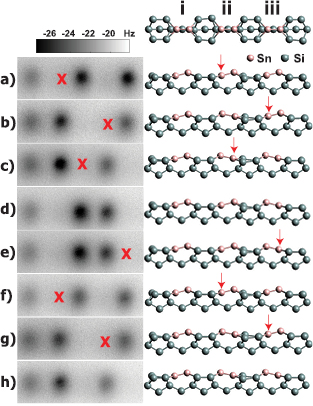
Figure 4. (Left) Constant height  f images showing controlled manipulation of the buckling state of dimers in a chain adsorbed on the Si(1 0 0) surface. Note that only the 'up' atom of each dimer is imaged due to the difference in height between the two atoms. (Right) Side view of ball and stick model showing configuration of the Sn dimers in each scan. The crosses (left) and arrows (right) indicate the atom targeted for manipulation in each scan. (Top) Top down view of Sn chain ball-and-stick model and labelling of dimers. (a) Initial configuration. (b) Flip dimer ii. (c) Flip dimer iii. (d) Flip dimer ii. (e) No manipulation. (f) Flip Dimer iii (restores original buckling configuration). (g) Flip Dimer ii. (h) Flip Dimer iii. A0 = 200 pm,
  V. Data acquired at 5 K.
Download figure:
Standard image High-resolution imageIn figure 5 we present an analysis of the threshold force measured between the tip and sample required to initiate the dimer flipping. As noted above, we follow the same convention as in previous works, and plot the approach curves up to the point at which we detect the change in dimer configuration, as the change in the tip-sample potential means that the inversion to force is no longer reliable [11, 27, 44]. Upon retraction we note a uniformly larger tip-sample force, which indicates the tip is retracting over what is now the upper atom of the dimer. As for the manipulation of the silicon dimers of the surface, we observe a spread in the threshold force required to flip the dimer between different configurations (figure 5(a)). In these plots abbreviated captions indicate the direction of data acquisition with 'fwd' indicating a forward curve (i.e. tip approaching the surface) and 'back' indicating a backward curve (i.e. tip retracting from the surface).

Figure 5. Site-specific tip-sample force plotted against tip-sample distance (i.e. F(z)) for different locations, acquired during the dimer flip sequence shown in figure 4. (a) Threshold force required to initiate a change in dimer configuration, and same data for the reverse manipulation, for dimers ii and iii. Note forces after the change in configuration are not plotted as the force inversion is not well defined after the change in the tip-sample junction. (b) Variation in threshold force required to initiate the same change in dimer configuration. Here, the manipulations on each dimer were in principle identical, and therefore the variation in threshold force is most likely due to variation in the precise positioning of the tip over the down atom of the dimer. (c) Forces measured over the 'up' atoms of dimers i, ii and iii. In these cases no manipulation occurred. Note that the vertical position of the force minimum over i is significantly closer to the surface than for the other dimers, suggesting there is some conformational difference in the dimer. This is supported by the observation that attempts to flip dimer i failed, and no jump in force was detected during approach over the 'down' atom position (also plotted).
Download figure:
Standard image High-resolution imageIn figure 5(a) the plots labelled 'reverse' indicate that the manipulation is the reverse manipulation process (i.e. the manipulation restores the original buckling configuration after a earlier manipulation on the same dimer). In these instances a difference in threshold force could indicate that the energy barriers between the two configurations are not symmetric. However, we stress that we also see statistical variation between manipulation events that should in principle require the same force. This is demonstrated in figure 5(b) where plots labelled 'repeat' indicate near-identical manipulations over a dimer in the same configuration as the initial manipulation. These data suggest that the variation in the threshold force is as sensitive to the precise positioning of the tip over the target atom as to the local environment of the dimer. Nonetheless, we can clearly determine that for this tip the threshold force required to initiate the dimer flip lies between 100 and 400 pN.
In contrast, force spectroscopy performed on the up atoms of the dimers shows a uniform behaviour (figure 5(c)). We note that the dimer to the left of the image (dimer i) has a slightly different configuration to dimers ii and iii, as the minimum in the force curves is shifted approximately 50 pm towards the surface. While the almost identical magnitude of the force strongly suggests the same chemical identity of the atom, the difference in its bonding configuration is also confirmed by the failure of attempted manipulation of the dimer during force spectroscopy over the position of the 'down' atom. Most likely this difference arises from the positioning of the dimer close to what appears to be a surface defect. Importantly, we can exclude the possibility that the feature is a different material (such as an adsorbed OH group) due to the identical magnitude of the forces, and note that a single Sn atom should not only adsorb on top of the rows, but also be relatively unstable [2], neither of which match the properties of the feature identified as dimer i.
In figure 6 we highlight the reproducibility of this manipulation technique on another dimer chain, using a tip demonstrating slightly different contrast. In these plots we use the same naming and labelling conventions throughout as for figure 5. Although this tip systematically demonstrated larger tip-sample forces, and larger threshold forces required to initiate manipulation, we find that the spread in the force needed to initiate the manipulation in different configurations and at different positions is roughly the same, varying from approximately 400 pN–800 pN.
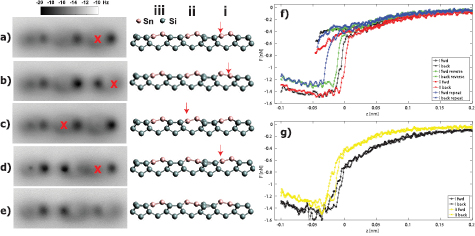
Figure 6. (Left) Constant height  f images showing controlled manipulation of the buckling state of dimers with a different tip. (Right) Side view of ball and stick model showing configuration of the Sn dimers in each scan. The crosses (left) and arrows (right) indicate the atom targeted for manipulation in each scan. (a) Initial configuration. (b) Flip dimer i. (c) Flip dimer i (restores original buckling configuration). (d) Flip dimer ii. (e) Flip dimer i. (f) Force curves acquired during dimer flips. (g) Force curves acquired over 'up' atoms of dimers. A0 = 200 pm,
  V. Data acquired at 5 K.
Download figure:
Standard image High-resolution imageAfter the controlled manipulation experiments shown in figure 6, we acquired a three-dimensional dataset over the same chain by performing a series of constant height scans at decreasing tip-sample separation in 7 pm intervals, the results of which are shown in figure 7. Similar to the bare Si(1 0 0) surface, at larger tip-sample separations we first observe the buckled structure, while upon close approach we observe uncontrolled manipulation of the dimers during the scan. As a result of this uncontrolled manipulation an apparent symmetric appearance of the dimers is observed. Analysis of the  f(z) curves acquired from the 3D dataset shows a similar trend to that acquired during single
  f(z) spectroscopy curves, with a jump in frequency shift observed over the down atom of the dimer.
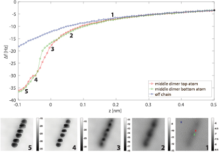
Figure 7.  plots extracted from 3D
  f dataset over atoms of Sn dimer, and over the Si substrate. Plotted below the graph are representative constant height
  f images extracted from the dataset at the heights labelled 1–5 on the graph. The position of the
  plots is marked by the crosses on image 1.
  plots are averages taken over a
  pixel area. A0 = 200 pm,
  V. Data acquired at 5 K.
Download figure:
Standard image High-resolution image4.3. Coupling and stability of the chains
A key result of the manipulation experiments presented in figures 4–6 is that the Sn dimers appear to be relatively well decoupled from each other, as mechanical perturbation of one dimer does not seem to affect the buckling structure of adjacent dimers. This is in contrast to the behaviour of adjacent silicon dimers within the dimer rows of the surface, which exhibit a high degree of mechanical and electronic coupling. Although an analysis of how the strain field is modified during buckling is beyond the scope of this investigation, intuitively this difference may be understood by considering that each dimer in the Sn chain is spaced from the others by an entire silicon dimer row. The mechanical and electronic coupling across the dimer rows is much weaker than than along the rows, and this spacing may serve to decouple the Sn dimers. Perhaps somewhat more surprising is the analysis of the effect of the manipulation on the silicon surface. In figure 8 we show images taken from the same manipulation sequence as figure 4, but filtered to remove high-frequency noise, and presented in a reverse colour scale, to improve contrast. By thresholding the image to highlight the silicon surface, it is possible to see that manipulation of the buckling state of the Sn dimers does not appear to modify the buckling configuration of the underlying silicon substrate. This is particularly surprising given the direct mechanical coupling of the Sn atoms to the underlying silicon dimers, and the well-known sensitivity of the silicon dimers in the rows to modifications in the strain field even at relatively large distances. Presumably either the intrinsic barrier to perturb the underlying substrate remains too high to surmount at 5 K, or the barrier is artificially raised by pinning of the dimer position, perhaps due to the bonding to the subsequent Sn dimer in the chain. This is somewhat contrary to results on higher coverage surfaces, where Sn chains have been shown to pin the buckling of other nearby chains [2], presumably via a strain interaction through the silicon surface.
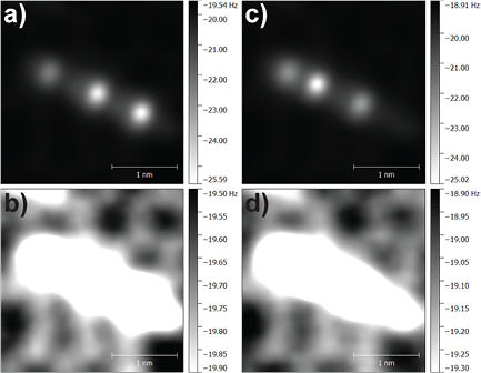
Figure 8. Filtered (20 pt gaussian) constant height  f images of Sn dimer chain on Si(1 0 0) (NB: plotted in reverse colour scale to improve contrast (white features are more attractive)). Taken from the same dataset as figure 4. (a) Original chain configuration, (b) Same image, colour scale adjusted to show silicon surface. (c) Chain configuration after two controlled dimer flips. (d) As (c), but showing surface state. Note that despite reversing the buckling configuration of two dimers in the chain the configuration of the silicon dimers of the surface is unchanged. A0 = 200 pm,
  V. Data acquired at 5 K.
Download figure:
Standard image High-resolution image4.4. Stability of the buckling state at intermediate temperatures
In figure 9 we present a dataset acquired at 78 K, consisting of data taken from a series of constant height slices acquired at decreasing tip-sample distance. Far from the surface (figure 9(a)) the chain images as diffuse attractive features. By applying a moderate low pass filter it is nonetheless possible to see small changes in the location of the minima of the images (highlighted in figure 9(c)). Because of the extremely weak interaction at this distance (particularly over the down atom of the dimer) we interpret these features as changes in the buckling state of the dimer chain occurring without mechano-chemical manipulation via interaction with the tip. Scans at close approach confirm that manipulation via chemical interaction with the tip can still occur, but only seems to occur approximately 80–100 pm closer to the chain (figure 9(b)) than the sequence shown in figure 9(a). While we cannot conclusively rule out some kind of modification of the energy barriers of the system due to a long-range interaction with the tip (perhaps via some kind of long-range electrostatic or dipole interaction) this data suggests that the energy barriers of the system are such that some residual thermal flipping of the dimers still occurs at 78 K. As briefly mentioned in discussion of figure 2(d), at close approach this tip demonstrates a mix of attractive and repulsive features. This mix of features is non-trivial to interpret as it does not fit the contrast predicted by either a 'pure' attractive or repulsive model. We speculate that this contrast is connected to the charge transfer that occurs between the upper and lower atoms of the dimers, and how this distorted charge distribution interacts with tips that are only partially passivated (perhaps by metal atoms adsorbed from the chains). We stress however that a definitive interpretation of this contrast mode will nonetheless require significant input from ab initio simulation methods.

Figure 9. Filtered (9 pt gaussian) constant height  f images of Sn dimer chain on Si(1 0 0) (a) Contrast far from chain at decreasing tip-sample height. At all heights the chain images as a diffuse attractive feature. (b) Same chain imaged at close approach. At this distance internal contrast in the chain is seen, and individual (indicated by red arrow), or multiple dimers are mechanically manipulated during the scans (c) Line profiles of normalised
  f taken across the chain in the weakly interacting regime. Arrows indicate where changes occur in the chain between different scans. A0 = 200 pm,
  V. Data acquired at 78 K.
Download figure:
Standard image High-resolution image
5. Discussion
By considering the literature of ab initio simulation of metal chain formation and structure, and specifically the energies calculated in these studies, some insight may be gained with regards to the experimental results presented above. The energy barrier for thermally activated flipping of the Sn dimer has been estimated at between 0.06 eV (for an isolated dimer) and 0.16 eV (for a dimer forming part of a chain) [16]. This should be compared to barriers calculated for the native silicon dimers of around 0.2 eV [11, 12]. Consequently, it should be expected that the Sn dimers are somewhat less stable than the silicon dimers at the same temperature. Qualitatively this matches our results, since we do not observe changes in the silicon dimer buckling at 78 K in clean regions of the surface, except at very close approach when we mechanically perturb the dimers. However, we note that using these figures in a simple Arrhenius estimation of the lifetime for the flipping suggests a rocking rate on the order of 100 Hz for the Sn dimers. Since the rocking we observe is detectable in scans taking on the order of 10 to 30 min (i.e. a sub-Hertz rocking rate), it seems likely that these barriers are somewhat under estimated. We must also highlight that similar to the intrinsic silicon dimers, there is likely to be significant variation in the barriers as a result of the local strain in the surface, and that our observations must be considered in the context of observed buckling in some Sn dimer chains at room temperature. As discussed in Glueckstein et al [2] buckling at room temperature was only observed for chains which had neighbouring chains within two lattice spacings, suggesting that the buckling was pinned in a similar fashion to the pinning of the Si dimers of the surface by adsorbates and defects. This raises interesting questions as to how the dimer flipping behaviour we observe may differ for samples with a higher Sn chain coverage, and also as to how the strain field between the chains might operate given our failure to observe any perturbation of the surface after flipping the Sn dimer states.
6. Conclusions
We have presented data demonstrating the controlled manipulation of the buckling configuration of Sn dimers on the Si(1 0 0) surface using mechano-chemical means, at 5 K. Our results show the Sn dimers to be surprisingly well decoupled, both from the other dimers in the chain, and the surface dimers of the silicon surface. As a result the buckling configuration of the chains can be controlled arbitrarily, unlike the dimers of the rows on the Si(1 0 0)-c( ) surface. We have measured the threshold tip-sample force required to initiate the confirmation change for different tips, and shown how the dimers assume an apparent symmetric structure when imaged at close approach, similar to the Si(1 0 0) surface dimers. At intermediate cryogenic temperatures we are able to observe changes in confirmation at a tip-sample distance that should preclude tip-induced manipulation. This suggests the energy barrier between buckling states for the Sn dimers can be surmounted even at 78 K.
Acknowledgments
AS gratefully acknowledges funding via the award of Leverhulme fellowship ECF-2013-525. We acknowledge funding from the European Commissions Marie Skodowska-Curie Actions, project reference ACRITAS- 317348—Ares(2016)909492.