

Abstract
The hole transport properties of heavily doped 4H-SiC (Al) layers with Al implanted concentrations of 3 × 10²⁰ and 5 × 1020 cm−3 and annealed in the temperature range 1950–2100 °C, have been analyzed to determine the main transport mechanisms. This study shows that the temperature dependence of the resistivity (conductivity) may be accounted for by a variable range hopping (VRH) transport into an impurity band. Depending on the concentration of the implanted impurities and the post-implantation annealing treatment, this VRH mechanism persists over different temperature ranges that may extend up to room temperature. In this framework, two different transport regimes are identified, having the characteristic of an isotropic 3D VRH and an anisotropic nearly 2D VRH. The latter conduction mechanism appears to take place in a rather thick layer (about 400 nm) that is too large to induce a confinement effect of the carrier hops. The possibility that an anisotropic transport may be induced by a structural modification of the implanted layer because of a high density of basal plane stacking faults (SF) in the implanted layers is considered. The interpretation of the conduction in the heaviest doped samples in terms of nearly 2D VRH is supported by the results of the transmission electron microscopy (TEM) investigation on one of the 5 × 1020 cm−3 Al implanted samples of this study. In this context, the average separation between basal plane SFs, measured along the c-axis, which is orthogonal to the carrier transport during electrical characterization, appears to be in keeping with the estimated value of the optimal hopping length of the VRH theory. Conversely, no SFs are detected by TEM in a sample with an Al concentration of 1 × 1019 cm−3 where a 3D nearest neighbor hopping (NNH) transport is observed.
Export citation and abstract BibTeX RIS
1. Introduction
Aluminum is the preferred acceptor dopant in both 4H-SiC bulk crystals and epi-layers when very high acceptor concentrations are needed. An elevated density of Al acceptors in SiC, like for any other dopant in a semiconductor lattice, brings to the formation of an impurity band (IB) and thus to a carrier transport through localized states. Above a given doping level, which depends on the semiconductor material, the transition to a metallic conduction is expected (semiconductor-to-metal transition, SMT). At the same time, in the case of implanted dopants the allocation of impurity atoms in the semiconductor lattice sites till the solid solubility at the post implantation annealing temperature, and the precipitation of the impurity atoms in excess with respect to this solubility limit, bring to the formation of structural defects that may influence the features of the carrier transport. Under the driving force of the technological interest for a high p-type doping of SiC, the features of the carrier transport in such a complex systems are under investigations. Because the critical density for the SMT has been estimated to be 6–8 × 1020 cm−3 in p-type 4H-SiC obtained by liquid phase epitaxy [1], this study has been performed by using 3–5 × 1020 cm−3 Al+ implanted 4H-SiC specimens and post implantation annealing temperatures as high as 2100 °C with the purpose to focus on their electrical properties at the semiconductor side of the SMT and on the effects of the IB conduction. The main knowledge and related algorithms that will be used for modelling the IB conduction in this study are resumed in appendix
In SiC doped by Al+ ion implantation, IB conduction has been detected by several authors. Namely, Heera et al [2] studied 4H-SiC samples with Al implanted concentration in the range 5 × 10¹⁹–1.5 × 1021 cm−3 (implantation temperature 400 °C) and 1670 °C/10 min post implantation annealing. These authors found that equation (A.1), consistent with the Miller and Abrahams model for the conductivity [3], could be used to fit the temperature dependence of the conductivity data of all their samples with two energies: 90–150 meV attributable to  and 6–22 meV attributable to
  (see appendix
  values are congruent with the energy related to the hole freeze-out into Al impurities, indicating the occurrence of a hole transport into the valence band (VB) extended states. Differently, the
  ones are interpretable in terms of nearest neighbor hopping (NNH) between occupied and unoccupied acceptor sites (see appendix
2. Experimental
The samples used for this study are high purity semi- insulating (HPSI),  8° off-axis, 4H-SiC wafers implanted with Al+ ions at 300 °C with different ion-energy and ion-dose values so to obtain almost box shaped Al depth profiles of 3 × 10²⁰ and 5 × 1020 cm−3 close to the wafer surface [9–12]. The implantation schedule was decided by using the simulation code SRIM2008 [13] and verified by secondary ion mass spectrometry (SIMS) measurements (for SIMS spectra see [14]). The implanted Al electrical activation was obtained by very high temperature treatments after that sample surfaces were protected by a resist film pyrolyzed at 900 °C in forming gas [15]. Annealing temperature and time were 1950 °C/5 min and 2000 °C/30 s for all the specimens, moreover one 5 × 10²⁰ Al cm−3 implanted sample was annealed 2100 °C /30 s. Two heating technologies were used: samples in contact with a radio-frequency inductively heated material for the 1950 °C processes (shortly called conventional annealing, CA), and samples in close contact with a microwave heated n-type SiC dummy specimens [16] for the 2000–2100 °C processes (shortly called microwave annealing, MWA). Major differences between these two technologies are heating and cooling rates by far larger during MWA than during CA. It is worth noting that both these rates are in turn larger than those of resistive furnaces by order of magnitudes. Main processing parameters for each sample of this study are listed in table 1.
Table 1. Main processing parameters and results of the RT electrical characterizations of the low resistivity p-type 4H-SiC specimens selected for this study. Sample names and corresponding symbols for all the figures of this work, are also given.
| Sample | Symbols in all the figures | Scheduled Al plateau (SRIM2008) (cm−3) | Implant temperature (°C) | Measured Al plateau (SIMS) (cm−3) | Heating technology | Annealing temperature (°C) | Annealing time (min) | RT Hall hole density,  (cm−3) (cm−3) |
RT resistivity (Ω cm) |
|---|---|---|---|---|---|---|---|---|---|
| SiC293e | ▴ | 3 × 10²⁰ | 300 | 2.94 × 10²⁰ | CA | 1950 | 5 | 5 × 10¹⁹ | 0.052 |
| SiC293a | ▵ | 3 × 10²⁰ | 300 | 2.94 × 10²⁰ | MWA | 2000 | 0.5 | 6 × 10¹⁹ | 0.059 |
| SiC296e | • | 5 × 10²⁰ | 300 | 5.34 × 10²⁰ | CA | 1950 | 5 | 1.4 × 10²⁰ | 0.031 |
| SiC296c | ○ | 5 × 10²⁰ | 300 | 5.34 × 10²⁰ | MWA | 2000 | 0.5 | 3.5 × 10²⁰ | 0.023 |
| SiC296b | * | 5 × 10²⁰ | 300 | 5.34 × 10²⁰ | MWA | 2100 | 0.5 | 4.5 × 10²⁰ | 0.021 |
The samples for electrical characterization were square van der Pauw (vdP) devices of 5 mm side with triangular Ti/Al based ohmic contacts on the four corners. The recipe for these contact preparation and the characterization of their ohmic behavior has been published in [17]. The electrical data were corrected to account for the effects due to the contact dimension with respect to the vdP device dimension as suggested in [18].
The vdP devices have been characterized in the temperature range 8–680 K by sheet resistance and Hall effect measurements. The latter have been performed by using 0.8–1 T magnetic fields. The sheet resistance values have been multiplied by the thickness of the half maximum full width (HMFW) of the as-implanted Al depth profiles to obtain the resistivity of the implanted layers. HMFW values have been obtained by the simulated and/or measured Al depth profiles. With respect to our previous study [4], the original part of the electrical characterizations of this work concerns the temperature region between 8 and 100 K. In this temperature range, contacts resulted still ohmic although in a narrower current range and for lower current values with respect to what found at higher temperature. At these low current values, Hall effect resulted hardly measurable owing to the small amplitude of the Hall voltage and to the low value of the signal-to-noise ratio. For these reasons, only sheet resistance measurements were reliably performed and are here reported.
To carry out the low temperature measurements, the samples were mounted in a closed cycle helium cryostat: because in this work the measure of the temperature is crucial, an additional calibrated detector was preliminary used to measure the holder temperature at the sample position. The measurements were performed in vacuum, at steady temperatures, by cooling (or heating, after rapid cooling to low temperature) the sample with different rates, to test the reproducibility of the transport data, and to exclude that the temperature dependence of the resistivity, here pointed out and discussed, could be significantly affected by unexpected non-equilibrium occupancy of electrically active defects. Such a test is due for the purpose of reliable interpretation of the experimental curves, especially at low temperature, in samples containing disorder, although such an approach unavoidably increases the scattering of the data. Magnetoresistance and photoconductive effects under white light have also been excluded at, and below, RT.
Finally, structural and compositional characterizations of a sample implanted with 5 × 10²⁰ Al cm−3, and annealed at 1950 °C for 5 min (sample SiC296e of table 1) have been carried out by (1 0 − 1 0) cross-sectional transmission electron microscopy (TEM), annular dark-field scanning transmission electron microscopy (ADF-STEM) and energy dispersive x-ray spectroscopy (EDS) using a FEI Tecnai F20 ST transmission electron microscope operating at 200 kV. A further sample with a considerably lower value of the Al plateau concentration (1 × 1019 cm−3) and submitted to the same post implantation treatment used in the case of sample SiC296e, has also been investigated by TEM for purpose of comparison.
3. Results and discussion
Table 1 shows, for each sample, the room temperature (RT) Hall hole density and the resistivity of the Al implanted layers. The former increases while the latter decreases for increasing both the implanted Al density and the post implantation annealing temperature, indicating a more efficient p-type doping with increasing values of these two processing parameters.
The temperature dependence of the resistivity data of all our samples is shown in the Arrhenius plots reported in figures 1(a) and (b). Each  curve in figure 1(a) was obtained with measurements from about 10 K to about 680 K. An enlarged view of figure 1(a) around the high temperature region is shown in figure 1(b). In a previous study [4] it has been shown that, around RT, the electrical properties of all the samples of table 1 are characterized by a parallel conduction phenomenon, owing to transport mechanisms that take place through valence band (VB) extended states and through localized states in an Al impurity band. Generally, in a heavily doped semiconductor at the semiconducting side of the SMT, a transition from the prevalence of one regime on the other is observed on decreasing the temperature, giving rise in the resistivity (or conductivity) Arrhenius plots to linear regions with different slopes, in agreement with the predictions of the Miller and Abrahams's model [3]. At low temperatures and for Al implanted concentrations up to about 1 × 1020 cm−3, such a transition between two linear behaviors has been actually observed in the Arrhenius plots of 4H-SiC 1950 °C/5min post implantation annealed specimens, and the mechanism for the transport in the IB has been identified as NNH [4]. At the higher doping level considered in this study with respect to [4], the resistivity Arrhenius plots do not evidence any linear behavior, neither at high, nor at low temperatures, as shown in figures 1(a) and (b). At the highest temperatures, around and above RT (see figure 1(b)), the presence of the mixed conduction between VB and localized states [4], and the doping induced reduction of the acceptor ionization energy [19] can justify the failure to observe a linear behavior related to the transport into the VB. At the lowest temperatures, instead, the sub-linear behavior of the resistivity data in the Arrhenius plots unavoidably leads to rule out the occurrence of a NNH transport in the IB. In [4], the conductivity data of the lowest doped sample of the present study, i.e. sample SIC293e of table 1, were already analyzed and found to be consistent with a 3D VRH transport mechanism. In this work, we will show that the low temperature conductivity data of all the samples of this study having Al doping level greater or equal to 3 × 1020 cm−3 may be interpreted in terms of a VRH mechanism. In the framework of the VRH theory, the analysis of the experimental data here obtained at the highest Al doping levels will lead us to explore the possibility of the existence of a conductivity mechanisms beyond the usual 3D carrier transport.

Figure 1. Arrhenius plots of the experimental resistivity data of the samples of table 1 in the temperature ranges 8–680 K (a) and 250–680 K (b). The symbols used to mark the data are those shown in table 1.
Download figure:
Standard image High-resolution image3.1. Fits of the conductivity data
3.1.1. Identification of the temperature ranges where a single conduction mechanism is dominant.
Assuming a temperature dependence of the conductivity  given by equation (A.1) with temperature independent pre-exponential factor, the determination of the active conduction mechanism reduces to the determination of the exponent 1/n of the exponential term. However, as different conduction mechanisms may be present in the whole temperature range here considered, one has to define in advance the temperature ranges that limit the quantitative analyses of the conductivity data. A simple way to accomplish this preliminary study is to calculate the temperature dependence of the derivative
  . In fact, if equation (B.1) holds true, such a derivative equals
  , thus, in a plot of the function
 ![$\text{Log}\left[\text{dln}(\sigma )/\text{dln}(T)\right]$](https://content.cld.iop.org/journals/0953-8984/29/3/035703/revision1/cmaa4aa5ieqn011.gif) versus
versus  , linear behaviors identify the temperature regions where equation (B.1) is valid, and the slopes of the linear traits correspond to −1/n values. It is worthwhile noting that a slope equal to −1 describes a simple exponential law, as it is for the NNH transport [4].
The logarithmic derivatives of the reciprocal of each curve of figure 1 are plotted in figures 2(a) and 2(b), (c) for samples with implanted Al concentration of 3 × 1020 cm−3 and 5 × 1020 cm−3, respectively. To minimize the effect of data fluctuations, which are strongly amplified by the numerical derivative, experimental data were smoothed before the latter calculation. Various straight lines of specific slopes q, are also traced in figures 2(a) and (b), with the purpose to recognize the temperature regions where different transport mechanisms prevail. The main result of this analysis is the appearance of slopes q of absolute value lower than 1, showing the departure of the data from the NNH behavior. In fact, only just above T = 350 K and over a narrow temperature region, the data in figure 2(a) approach a slope q = −1. By observing the data of figure 2(b), this temperature region seems to be further reduced at the highest Al doping level. Above such a temperature region, additional transport mechanisms are present, giving rise to mixed conduction effects involving VB extended states. These effects, which appear in figures 2(a) and (b) as curves locally showing either positive or negative slopes, will not be further discussed in the present context as, not corresponding to simple exponential behaviors, they cannot be analyzed through the derivative  . Below 350 K, the data of the heaviest doped samples in figure 2(b) follow slopes q ~ − (0.3–0.33) that are quite different from the Mott's law value where q = −0.25. In figure 2(c), the logarithmic derivative of the conductivity was reported in log–log plot as a function of the temperature for the heaviest doped sample only (sample SiC296b of table 1): in this sample, the data are compatible with the further persistence of the linear trend up to about 500 K. To better evidence the departure from the q = −0.25 slope, the data of figure 2(c) relative to the heaviest doped sample were fitted in the temperature range T ⩽ 500 K with a linear function: in the fitting, the slope of the line was either leaved to vary as free parameter or fixed at the value q = −0.25. The best-fit slope resulted q = −0.31, an absolute value of the slope higher than the one of the Mott law, q = −0.25, as asserted above. The slope resulted even higher (q = −0.33) if the analysis was limited to the temperature rangeT ⩽ 350 K. At variance, for the lower doped samples of figure 2(a), the data of the logarithmic derivative are consistent with a VRH mechanism only below 180 K, but the possibility to decide between the previous two slope values is hindered by the large spread of the data. The conclusion of this preliminary study based on the data reported in figures 2(a) and (b), is twofold. On the one hand, the conductivity of the Al implanted samples of table 1 may be modelled over given temperature ranges by a VRH mechanisms with temperature independent pre-exponential factor
  (equation (B.1)). On the other hand, except for the lowest doped sample, n always approaches the value of 3. To the best of the author knowledge, the latter VRH regime has never been previously detected in 4H-SiC. Moreover, the temperature range where this phenomenon appears extends up to and above RT.
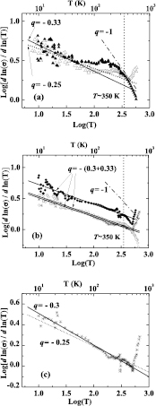
Figure 2. Plot of ![$\text{Log}\left[d\ln (\sigma )/d\ln (T)\right]$](https://content.cld.iop.org/journals/0953-8984/29/3/035703/revision1/cmaa4aa5ieqn015.gif) versus
versus  for the samples of table 1; the corresponding temperature scale is reported on the top axis. The absolute value of the slope q of the linear traits gives the inverse of the hopping exponent 1/n. (a) Samples with Al implanted density of 3 × 1020 cm−3: (empty triangles) 2000 °C/30 s, (full triangles) 1950 °C/5 min. For comparison, continuous, dot and dashed-dot straight lines with q −0.33, −0.25, and −1, respectively, are also shown. (b) Samples with Al implanted density of 5 × 1020 cm−3: (full circles) 1950 °C/5 min, (empty circles) 2000 °C/30 s, (stars) 2100 °C/30 s. Continuous straight lines show the linear best fits of the data, having q in the range −(0.3–0.33). For comparison, a dashed-dot line with q = −1 is also shown. In both (a) and (b): the vertical short-dash line at 350 K indicates an approximate temperature around which the slope −1 seems to prevail on the other ones, which could suggests that NNH conduction is prevailing over the VRH one. (c) Stars: temperature dependence of the logarithmic derivative of the conductivity reported in Log-Log plot for the 5 × 10²⁰ Al cm−3—2100 °C/30 s sample. Continuous line: linear best-fit of the data in the temperature range 9–500 K, with slope q = −0.31 (R2 = 0.95). Dotted line: linear best-fit of the data in the temperature range 9–500 K, with slope for q = −0.25 (R2 = 0.91).
Download figure:
Standard image High-resolution image3.1.2. Analysis of the conductivity data through the generalized Mott law over a given temperature range.
The results of the previous analysis (figures 2(a) and (b)) have been used to select for every Al implanted sample of this study the temperature interval where a single hopping regime can be assumed, so that equation (B.1) can be applied to fit the temperature dependence of the conductivity data (without any preliminary smoothing procedure). Because, in the experimental temperature range, the conductivity varies of several orders of magnitude the fitting function was taken in the form:

The meaning of the free parameters  ,
,  and
and  can be deduced by the comparison with equation (B.1) rewritten in the form:

so that:  and
and  , where
  is assumed temperature independent. In this way, the relative discrepancy between theoretical function and experimental data are nearly equally weighted at any temperature. From the previous analysis, the fit to equation (2) of the conductivity data was then limited to temperatures T < 500 K for the heaviest doped sample (sample SIC296b of table 1, with 5 × 10²⁰ Al cm−3 and MWA at 2100 °C/30 s), to T < 350 K for the average doped samples (samples SIC296e and SIC296c of table 1, with 5 × 10²⁰ Al cm−3 CA at 1950 °C/5 min and MWA 2000 °C/30 s, respectively) and to T < 180 K for the lower doped samples (samples SIC293e and SIC293a of table 1, with 3 × 10²⁰ Al cm−3 every annealing). The
  outputs of the fitting process are reported in table 2, where the samples have been ordered from top to bottom for decreasing resistivity and increasing hole density at RT, according to the data of table 1. As shown in table 2, at the highest implanted Al density of 5 × 1020 cm−3, the exponent
  is found in the range 0.30–0.31 for all the specimens, according to the results of figures 2(b) and (c). At variance, for the samples with the lowest implanted Al concentration (3 × 1020 cm−3), whose analysis of the numerical derivative in figure 2(a) indicated a possible VRH mechanism but not resolved the n value, two different values of the exponent
  are obtained from the best fits in the chosen temperature range. Namely,
  ~ 1/3 for the sample SiC293a (3 × 1020 cm−3 and MWA 2000 °C/30 s) and
  ~ 1/4 for the sample SIC293e (3 × 1020 cm−3 and CA 1950 °C/5 min). Most probably, at this critical doping level, the different post-implantation treatments are at the origin of this different behavior. We note here that within the chosen temperature ranges the fit parameters resulted stable and independent of the initial conditions.
Table 2. Free parameters  ,
,  , and
, and  obtained by the fitting of the conductivity data of the samples of this study by equation (1) in the temperature range indicated (see text). Tmax is the superior limit of the temperature range considered in the fit.
  is the adjusted R-square.
| Sample | Tmax (K) | P1 | P2 | P3 | R2 |
|---|---|---|---|---|---|
| SiC293e | 180 | 12.0 ± 0.7 | 35.5 ± 0.3 | 0.23 ± 0.01 | 0.997 |
| SiC293a | 180 | 7.26 ± 0.15 | 31.3 ± 0.1 | 0.329 ± 0.005 | 0.999 |
| SiC296e | 350 | 9.6 ± 0.2 | 33.3 ± 0.1 | 0.297 ± 0.006 | 0.998 |
| SiC296c | 350 | 7.57 ± 0.05 | 22.28 ± 0.04 | 0.309 ± 0.003 | 0.9997 |
| SiC296b | 500 | 7.68 ± 0.06 | 21.5 ± 0.08 | 0.304 ± 0.003 | 0.999 |
Figures 3(a) and (b) show the plots of ln(σ) versus 1000/T, together with the calculated fits based on equation (2) (free parameters of table 2) and extrapolated to the full temperature range of measure. Figure 3(a) shows that a good fit to the experimental data is found for all the samples at least up to 180 K. However, the enlarged view given by figure 3(b) evidences that only for the samples with the lowest conductivity the theoretical curves fit nicely the data up to about 350 K. Finally, only for the sample with the highest Al implanted concentration the agreement persists up to about 500 K. Such an extension of the VRH transport up to so high temperatures is consistent with the assumption of a hopping model for non-interacting carriers, notwithstanding the electron–electron interaction plays a significant role in a doped semiconductor (see appendix  value toward a lower one, for increasing doping level, appears then confirmed by the above analysis and cannot be ignored.

Figure 3. Arrhenius plot of the experimental conductivity data and corresponding theoretical curves in the full temperature range (a) and above 200 K (b). The symbols used to mark the experimental data are in agreement with those reported in table 1. The continuous lines give the best fits of each experimental curve extrapolated to the full temperature range of measure. The theoretical curves were obtained through the function:  , using the parameters reported in table 2. The short-dash vertical lines in (a) and (b) correspond to 180 K and 350 K, respectively.
Download figure:
Standard image High-resolution imageIn the framework of the VRH theory for non-interacting carriers, deviations of  from the usual value of 4 can be explained either in terms of a reduced dimensionality of the mechanism, or in terms of an energy dependent density of localized states in proximity of the FL [20–22]. In the latter case, following the approach given in Ref. [19, 22], a value around
  would imply a density of localized states in proximity of the FL with an energy dependence given by a power law with an exponent around s = 1/2, as it results by putting this
  value in the following expression [20]:
  (see appendix
  dependence is surprising. Conversely, the assumption of a constant
  , as for non-interacting carriers, may be thought to be a reasonable approximation of a Gaussian distribution function of the localized states for a large energy range around the maximum of the IB. Then, in what follows, instead of considering a
  dependent density of localized states, we will try to investigate the possibility to find an experimental support to the hypothesis of a strong anisotropic transport, consistent of a 2D VRH, through a structural analysis of the implanted and annealed layers. The
  and
and  parameters will be evaluated according to such an assumption, to test the self-consistency of the overall results.
3.1.3. Evaluation of the optimal parameters of the VRH transport.
In order to estimate the hopping parameters (optimal band width and optimal length) for these samples through the equations of appendix  parameters in table 2 are close to the expected values of 1/4 and 1/3, for 3D and 2D VRH, respectively, the linear fits have been recalculated by fixing
  values to these fractions. According to equations (1) and (2), the recalculated
  and
and  values are presented in table 3, as
  and
and  , respectively. This analysis is equivalent to search a linear trait in the plot of the experimental conductivity data in ln-scale as a function of either
  or
or  . These plots are reported in figures 4(a) and (b).
Table 3. VRH conduction parameters  ,
,  ,
,  and
and  at 10 K, and
  (see the text) are the outputs of the analysis of the electrical conductivity data by equation (2) assuming exact value n = 3 or 4 (see the text). Tmax is the superior limit of the temperature range considered in the fit. In the last column, the unit length
  is 'cm'.
  is the adjusted R-square.
| Sample | Tmax (K) | n |  (Ω−1 cm−1) (Ω−1 cm−1) |
T0 (K) | R2 | Ropt/ξ at T = 10 K |  at T = 10 K (meV) at T = 10 K (meV) |
g (µ) (eV−1 cm1−n) | 3D density of sites at T = 300 K (cm−3) |  (cm) (cm) |
|---|---|---|---|---|---|---|---|---|---|---|
| SiC293e | 180 | 4 | (5.93 ± 0.35) × 104 | (1.53 ± 0.02) × 106 | 0.997 | 7.42 | 4.26 | 0.137/ξ3 | 0.0084/ξ3 | — |
| SiC293a | 180 | 3 | (1.26 ± 0.03) × 103 | (3.09 ± 0.02) × 104 | 0.999 | 4.86 | 4.19 | 3.23/ξ2 | — | — |
| SiC296e | 350 | 3 | (5.09 ± 0.09) × 103 | (4.02 ± 0.01) × 104 | 0.998 | 5.30 | 4.57 | 2.49/ξ2 | 0.06/ξ3 | 8 × 10⁻⁸ |
| SiC296c | 350 | 3 | (1.29 ± 0.02) × 103 | (1.193 ± 0.004) × 104 | 0.9996 | 3.54 | 3.05 | 8.39/ξ2 | 0.22/ξ3 | 9 × 10⁻⁸ |
| SiC296b | 500 | 3 | (1.33 ± 0.01) × 103 | (1.087 ± 0.007) × 104 | 0.999 | 3.43 | 2.96 | 9.18/ξ2 | 0.24/ξ3 | 8 × 10⁻⁸ |

Figure 4. Temperature dependence of the experimental conductivity data: (a) plotted as  versus
  for the 3 × 1020 cm−3 Al implanted CA annealed sample and (b) plotted as
  versus
  for all the other samples of table 1: (triangles) 3 × 1020 cm−3 Al implanted samples; (circles and stars) 5 × 1020 cm−3 Al implanted samples; stars, empty and full symbols refer to 2100 °C/30 s, 2000 °C/30 s and 1950 °C/5 min annealing, respectively. Vertical short lines mark the temperatures T = 500 K, T = 350 K and T = 180 K, below which the curves of the sample SiC296b, the couple of samples SiC296c and SiC296e and the sample SiC293a, respectively, show a linear trend (see text).
Download figure:
Standard image High-resolution imageThe inspection of  ,
,  ,
,  parameters of table 2 and n,
  and
and  values of table 3 may show a dependence on the sample processing parameters. The reference temperature
  and reference conductivity
  may depend on both the electrical activation of the implanted Al impurities and the degree of structural order of the implanted layer, being calculated from a fit of experimental conductivity data that depend on such parameters. Starting with the reference temperature
  a comparison of its values with those of the RT Hall hole density,
  in table 1, shows that for a fixed implanted Al concentration,
  increases on decreasing
  values, thus appearing to be inversely related to the electrical activation degree of the Al impurities. This supports the assumption that the energy states involved in the hopping process correspond to the Al acceptor levels broadened into an IB, rather than localized states introduced by structural defects. As to the conductivity at infinite temperature,
  , we may compare for each sample the
  data in table 1 with the
  values in table 3 and observe that in the latter table, in both the 3 × 10²⁰ Al cm−3 and 5 × 10²⁰ Al cm−3 cases, the
  values do not increase on increasing the RT hole density. This suggests that in our samples the degree of structural order influences
  more than the doping level. Then, with reference to the data in table 3, at a given implanted Al concentration, the higher
  values systematically observed in the case of the CA treated samples indicate the presence of a lower degree of disorder in these samples with respect to those annealed by MWA. We may also note that, in the case of sample SIC293e, both the
  and
and  parameters have their highest values indicating that differently from all the other samples of this study, a significant lower amount of both structural disorder and electrical activation is present in the Al implanted layer of this sample. A result consistent with these data has been shown in [8] for another sample of equal implant concentration 3 × 10²⁰ Al cm−3 and annealed at 1950 °C/10 min by CA. For this sample a n = 4 VRH behavior of the low temperature conductivity has been found, with higher
  and higher conductivity than the sample SIC293e, as for a higher doping level induced by annealing time increasing. Finally, it is worth noting that independently on the implant concentration and on the annealing temperature, all the samples annealed with MWA have a nearly identical and minimum
  value. This suggests that a similar and maximum degree of structural disorder is present in all these samples. Most probably, either the short annealing time or the high heating/cooling rates used in these MWA treatments have an adverse effect on the degree of structural order. In conclusion, owing to the higher annealing temperatures, the MWA conditions used in our samples seem to favor a better electrical activation of the Al impurities with respect to the CA treated samples, but also appear to introduce a higher structural disorder and a greater anisotropy in the transport properties.
The main hopping parameters, defined in appendix  and the average hopping energy,
  , are strictly related to the reference temperature T0 reported in table 3. Then, it is possible to evaluate individually
  ,
,  , and the density of the localized states at the FL
  , from the following relations (see appendix
where A is a constant equal to  and to
  when n = 4 (3D VRH) and n = 3 (2D VRH), respectively, and correspondingly
  , or
, or  . In equation (3),
  is the localization length. For purpose of comparison with literature data, the values of
  and
and  reported in table 3 have been calculated at a temperature of 10 K. At this temperature, the optimal energy
  is equal to a few meV, increasing to several tens of meV at T = 300 K, a value that approaches the impurity bandwidth. In fact, the latter can be roughly taken as comparable to the doping induced reduction of the acceptor ionization energy, which varies from a value of 220 meV for the dilute Al impurity in 4H-SiC, to a value of about 100 meV in samples with Al implanted concentrations of the order of 1020 cm−3 [4, 11]. This observation is consistent with the hypothesis of a VRH transport between Al impurities in substitutional sites. The values of
  , normalized to
  (d being the dimensionality of the VRH) are also reported in table 3 showing increasing values on increasing doping levels for samples of equal implanted Al concentration and equal n (see table 1). Then, the product
  , calculated at a given temperature, permits an estimation of the density of the sites involved in the hops. To compare this density for all the samples, a 3D value must be derived in the cases where the 2D VRH has been detected. To this purpose, the 2D
  density of table 3 has been divided by
  , which is the critical length in the VRH that qualifies the dimensionality of the mechanism. In fact, a 2D VRH is expected to appear when, in one direction of the space, the dimension of the space is comparable to the optimal length
  , so that in this direction the hops are practically inhibited. The values of the 3D density of sites, calculated at T = 300 K, are reported in table 3. As in the highest doped samples the VRH results to persist up to RT, it is possible to give a rough estimation of the localization length,
  , in these samples by equating the measured hole density
  to the 3D density of hopping sites. The last column of table 3 shows that
  results to approach one nanometer, as often assumed in the literature [24, 25]. More realistically, mixed conduction effect are expected to take place at RT [4], although the IB conduction can have a dominant role, so that
  should assume higher values. Taking
  independent of energy [19] and of a few nanometers,
  results to range from a few times
  (RT limit) to a few tens of nanometers (low temperature limit).
The analysis of the conductivity data of the Al implanted and annealed samples of this study indicates that a transition from a 3D to a 2D VRH transport mechanism could take place on increasing the p-type doping level associated with a higher Al concentration and with a higher post implantation annealing temperature. The dependence of the 2D VRH parameters of table 3 suggests that in such a transformation the increase of the lattice disorder plays a significant role, resulting in something like the 'size effect' recognized by Shklovskii and Efros in amorphous Ge films (see [19], p 217 etc).
3.2. Structural defects responsible of the dimensionality reduction of the observed 2D VRH mechanism
The identification in our samples of the possible origin of a 2D VRH transport mechanism would be of great support for the interpretation of the temperature dependence of the conductivity data. The proposed transport mechanism corresponds to a reduction of dimensionality that can be described by a strong path anisotropy between the in-plane hopping conduction and the carrier hops in direction perpendicular to the layer, approximately along the c-axis for the samples of this study. In the literature, a transition from 3D VRH to 2D VRH has been seen in amorphous semiconductor films of Ge on reducing the film thickness to a value comparable with the optimal hopping length, leading to a dependence of the parameter  on the film thickness [26–29]. The concept of 'size effect' has been given by Shklovskii and Efros in terms of percolation threshold, i.e. the critical length for the onset of long-range connectivity in a random system [19]. For the samples of table 3,
  is at most of the order of the tens of nanometers, which is significantly shorter than the thickness of the implanted layer
  where the current is flowing, i.e. about 0.4 µm in these samples. Then, the transition to a 2D VRH could appear only if the optimal hopping length becomes comparable to some characteristic lengths of the internal structure of the conducting layer (not to its thickness). Moreover, the previously discussed dependence of some of the parameters reported in table 3 on the degree of structural disorder suggests that this characteristic length could be related to the presence of lattice defects due to heavy Al implantations and post-implantation annealing processes.
As previously noted, it is well known that these Al+ implanted and annealed 4H-SiC samples may contain extended defects. For this reason, the possibility that the observed n = 3 VRH transport could be interpreted as an anisotropic transport originating from the lattice structure of these heavily doped layers has been investigated. A preliminary structural investigation by TEM, STEM and EDS has thus been undertaken on one of the samples implanted at the highest Al concentration of 5 × 1020 cm−3 and annealed at 1950 °C/5 min (sample SiC296e of table 1), i.e. the sample with the lowest doping level where a n = 3 VRH transport mechanism has been recognized. The results of this investigation are summarized in figure 5. In figure 5(a) [14], a (1 0 − 1 0) cross-sectional weak beam (WB) micrograph of the whole implanted layer is reported. Different types of defects inside the Al-implanted layer are observed. In the framework of this work, the most important defects are stacking faults (SF), i.e. faulted dislocation loops lying on the (0 0 0 1) basal planes and Al-related precipitates. In figure 5(a), the faulted loops are observed edge-on as white contrasted lines making an angle close to the miscut angle with the sample surface, their contrast arising from the partial dislocations that bound the loops. The SF depth distribution is not uniform and appears to peak close to the end of the Al implanted plateau region. In the (1 0 − 1 0) WB micrograph reported in figure 5(b), the Al concentration plateau region is shown at higher magnification. Defects with a projected hexagonal shape are clearly observed inside the Al plateau region with a rather wide size distribution. In the STEM image reported at even greater magnification in figure 5(c), these defects are just barely visible. To get insight on their composition and on the overall Al distribution inside the defective implanted and annealed layer, an EDS line profiles analysis has been undertaken across the main visible defects. An example of the results obtained by an EDS line profile across one of the hexagonal shaped defects whose edges have been marked with a dashed line in figure 5(c), is reported in figure 5(d). In this figure, circles and squares mark the intensity ratios of the C and Al to the Si K peaks, respectively. A clear Al accumulation is observed at the beginning of the profile indicating that these defects are connected to Al-related precipitates. The structure of these defects is rather complex and its study, currently underway, is beyond the scope of this work. We bound here ourselves to note that cavities like the black contrasted region observed in figure 5(c) along the AB line profile seems also to be systematically observed in connection with the Al-related precipitates. In figure 5(e), intensity ratios obtained by an EDS line profile A'B' (figure 5(c)) across the traces of two SFs, whose positions are marked by vertical lines, is reported. In this case, no sign of Al accumulation is detected revealing that their visibility in figure 5(c) is uniquely due to residual diffraction contrast. In summary, within the sensitivity limits of the EDS technique (~1 at%) the SFs appear not related to the Al precipitation phenomenon. The formation of interstitial type loops and SF lying in the  basal plane of heavy P or Al doped 4H-SiC after high temperature (⩾1800 °C) post implantation annealing is a phenomenon previously observed [30–33] thought to be an effective way to accommodate the lattice expansion due to the presence of implantation induced interstitial atoms. In [14], the formation of SF has been related to the overcoming of the Al solid solubility limit in 4H-SiC at the employed annealing temperature of 2 × 1020 cm−3 [34]. In our case, by focusing on the surface region where the SFs density is lower and the Al concentration is maximum and homogeneous, the average separation between SFs measured along the c axis is found to be of about 30 nm, i.e. of the same order of magnitude of the low temperature optimal hopping length
  , estimated from the analysis of the conductivity temperature dependence of these layers. This may suggest that space regions bounded by closely stacked SFs limiting the carrier hops, behave as channels for the hole transport thus leading to a dimensionality reduction, from 3D to 2D, of the VRH conduction. Here we note that this sort of steering of the carrier hops is essentially different from a quantum confinement of the hole wavelength.

Figure 5. Structural and compositional investigation of the sample SIC0296e of table 1. (a) and (b) (1 0 − 1 0) cross-sectional WB micrographs of the whole implanted layer (reproduced with permission from [14]. Copyright 2016. The Electrochemical Society) (a), and of the Al concentration plateau region (b). (c) STEM image of one of the defects with a projected hexagonal shape visible in (a) and (b); (d) intensity ratios of the C K (filled circles) and Al K (filled squares) to the Si K peak obtained by an EDS line profile, AB marked (c), across the defect whose edges have been marked with a dashed line in (c); (e) as in (d), the intensity ratios obtained by an EDS line profile, A'B' (see (c)), are reported. In (c) and (d) the spatial lengths are in nm. In this case, the line profile is taken across the traces of two stacking faults.
Download figure:
Standard image High-resolution imageTo verify this hypothesis a further cross-sectional TEM investigation has been carried out on a sample uniquely differing from the above described sample SiC296e by a considerably lower value of the Al plateau concentration, i.e. 1 × 1019 cm−3. In this case, the possible presence of SFs would rule out our previous hypothesis as in this sample the conduction has been found to obey to a 3D NNH mechanism [4]. In figure 6 [14], a cross-sectional (1 0 − 1 0) WB micrograph of the surface Al implanted layer is reported. In this micrograph, obtained with the very same WB setting used in the case of figures 5(a) and (b), basal plane SFs are not observed, small loops lying on lattice planes presenting in this sample orientation almost orthogonal traces, being uniquely visible (more details about the structure of the defects of figure 6 can be found in [14]). This finding just confirm the possibility of a close relation between the SFs presence and the proposed 2D conduction mechanism but further work is necessary to make a definitive conclusion.

Figure 6. (1 0 − 1 0) cross-sectional WB (−g,4g) g = [0 0 0 4] micrograph of the surface region of a sample with an Al plateau concentration of 1 × 1020 cm−3 annealed at 1950 °C for 5 min (reproduced with permission from [14]. Copyright 2016. The Electrochemical Society).
Download figure:
Standard image High-resolution image
In 4H-SiC, Iwata et al [35] theoretically found that Shockley SF can create quantum-well-like structures, giving rise to thin regions of the 3C-SiC poly-type, whose energy band gap is lower than that of 4H-SiC. In these structures, spatial confinement of the electron wavelength occurs in the direction of the c-axis, leading to quantized energy levels and a 2D electron gas localized in the stacking fault plane. However, because almost all the band gap difference between the 3C and 4H SiC poly-types appears in the conduction band offset [35], no spatial modulation of the VB, able to induce quantization of the energy levels in proximity of the VB top and quantum confinement for holes, should be expected.
In literature, several examples of conductor networks leading to long-range connectivity with dimensionality lower than 3 have been reported. In particular, it can be mentioned the VRH conduction controlled by a network of one-dimensional (lD) quantum wires in porous silicon [25, 36], VRH transport in amorphous insulating alloys [37] and in a class of doped nanocrystal solids, in particular, n-type semiconductors, where nano-particles of nanometer size are formed, giving rise to strong quantum confinement effects. These artificial solids behaves as an array of quantum dots (QD), whose radius sets the localization length of the hopping conduction. An example is given by CdSe QDs, having average radius of few nm, which have been investigated by Yu et al [38]. However, in most of these cases, disorder and nano-structuration play the main role in the onset of the hopping transport, whereas in the model here proposed hopping is supposed activated by heavy doping, while defects (disorder) are supposed to induce a dimensionality reduction of the transport. Finally, in granular metals, where arrays of metallic particles, of a size usually ranging from a few to hundreds of nanometers, are embedded into an insulating matrix [39, 40] a 3D VRH transport described by equation (B.1) with n = 2 has been observed. This finding is interesting in this contest as it suggests that in principle a VRH transport controlled by metallic precipitates provided of proper dimension and density cannot be excluded. In our case, where Al related precipitates have been observed, we can exclude such a situation because the observed VRH law, i.e. equation (B.1) with n = 3 or 4, is different from that found in granular metals in comparable ranges of temperature, i.e. equation (B.1) with n = 2 [38–40], persistent in some cases [39] even up to about 200 K.
4. Summary and conclusion
The results of resistivity measurements taken on heavily doped Al ion implanted 4H-SiC layers, with Al implanted impurity concentrations of 3 × 1020 cm−3 and 5 × 1020 cm−3, after post-implantation annealing at temperatures ranging from 1950 °C to 2100 °C have been analyzed to determine the transport mechanism responsible of their temperature dependence. The results of this analysis show that a semiconductor behavior is preserved in all the samples with typical features of a mixed transport between VB extended states and localized energy levels. The resistivity curves may well be described by a VRH mechanism over a wide temperature range. The sample with the lowest dopant concentration as well as the lowest annealing temperature exhibits a  temperature dependence in the exponential argument of the conductivity from 10 to about 200 K. The analysis of the transport mechanisms of all the other samples indicates a conductivity exponential argument proportional to
  from 10 K to about RT. An effort was made to point out the deviation of these experimental data from the more usual behavior predicted by the Mott law. This is consistent with a current transport by a nearly 2D system of non-interacting carriers. Trying to verify whether at the origin of this behavior there was a structural modification of the 4H-SiC implanted and annealed layers, a preliminary structural and compositional investigation of a sample with an Al concentration of 5 × 1020 cm−3 annealed at 1950 °C for 5 min, has been undertaken by TEM, STEM and EDS. The results of this investigation have shown the presence of Al-related precipitates and SFs lying in the 4H-SiC basal planes. Trying to correlate these observations with the results of the electrical transport, it has been found that the average spacing of the SFs along the c-axis is of the same order of magnitude of the low temperature value of the optimal length
  of the VRH transport mechanism. This may suggest the possibility that the presence of these planar defects confines the carrier hops in direction orthogonal to its flux. A further TEM investigation of a sample with an Al concentration of 1 × 1019 cm−3 also annealed at 1950 °C for 5 min, where a 3D NNH transport mechanism was known to be the main conduction mechanism, has shown the absence of any basal plane SFs in the Al implanted layer. This supports the possibility that these planar defects are actually responsible of the
  VRH transport inducing the strong anisotropy in the conductivity of the samples of this study. Further work will be made to reinforce such a conclusion. It is worth recalling that at the best of the author knowledge, the possibility of a similar 2D conduction regime has never been previously recognized in SiC.
Acknowledgments
Authors warmly acknowledge the work of Salvatore Vantaggio and Marco Gorni for their contribution to perform electrical measurements below room temperature. The microwave processing of the samples of this study was performed at the George Mason University of Fairfax (VA), during the fruitful and warmly acknowledged collaboration with Prof Mulpuri Venkata Rao, Dr Anindya Nath and Dr Yong-lai Tian, the last of LT-technologies. Authors are indebted with Dr Cesare Donolato for his helpful comments about this manuscript, and with Professor Alberto Carnera for SIMS measurements.
Appendix A.: IB conduction mechanisms and related algorithms
The transport by hopping among localized states in semiconductors has been investigated for a long time. In a homogeneous semiconductor, localized states can be induced both by lattice disorder, as band-tail states, and by doping as impurity levels located within the energyband-gap. In the former case, the increasing lattice disorder can progressively reduce the extension of the carrier wave function until spatial localization is reached (Anderson transition). In the latter case, the electron–electron interaction can play a relevant role in leading the system toward the transition to a metallic behavior (semiconductor-to-metal transition, SMT), which takes place when the net doping level exceeds a critical density, even in the ideal situation of a periodical impurity arrangement. In any case, at the semiconducting side of the SMT transition a hopping conduction through localized states generally appears in compensated semiconductors, which can manifest either as hopping between nearest neighbors (NNH) impurity sites, or as the so-called VRH, depending on the proximity to the critical density for SMT and on the temperature. The VRH can be observed at lower temperatures with respect to the NNH and, in principle, provided the temperature decreases enough, the VRH regime is always expected to replace the NNH conduction. However, the transition between the NNH and the VRH mechanisms appears at temperatures that increase on increasing the density of localized states [19]. The differences between NNH and VRH conduction processes have been clarified by Shklovskii and Efros [19] and by Mott [6, 7].
A pioneering theoretical description of the NNH has been given by the model of Miller and Abrahams [3], where a random resistance network is assumed to calculate the conductivity of a semiconductor. In this model, the following thermally activated law for the conductivity is proposed:

where:  is the Boltzmann constant,
  gives the conductivity into the band of extended states, whose temperature dependence is due to the carrier promotion from impurity states to conduction/valence band states, with an activation energy
  , while
  and
and  represent hopping conduction processes between localized impurity states, characterized by the activation energies
  and
and  , respectively. The energy
  describes the thermal activation for the hop of a carrier from an occupied impurity to another already occupied impurity (transition to the higher Hubbard IB), whereas the energy
  , characterizes the carrier hops from an occupied to the nearest unoccupied neighbor impurities (NNH). The density of unoccupied impurity doping atoms depends on compensation. Correlations among
  ,
,  , doping, and compensation effects have been proposed by different authors [3, 41, 42].
The VRH mechanism can be described, following Mott [7], as a hopping process between states lying in proximity of the Fermi level (FL),  , within an optimal energy band around
  , here called
  . In practice, in this hopping regime, the activation energy becomes a function of temperature as well. This description predicts an universal conductivity law like:

that is known as the Mott law when n = 4. In this case, the pre-exponential term  of equation (A.2) is the conductivity at infinite temperature, while
  is a reference temperature that depends on the energy state distribution around the FL,
  , assumed constant, and on the localization radius of the states close to the FL,
  . The latter is a length describing the spatial extent of the wave function localized at a single site, so that:
 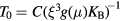 [6, 19]. The proportionality constant
  , entering in this definition of
  is a dimensionless parameter that depends on the details of the hopping site network assumed in the model of transport. It can be shown that equation (A.2) features the value n = 4 when considering the case of a three dimensional (3D) system of non-interacting carriers, with the assumption of both uniform energy distribution and degree of localization of the states involved in the hopping transport. However, equation (A.2) is a universal law, also applicable for a system of either interacting or non-interacting carriers of different dimensionality. In particular, for a two dimensional (2D) system of non-interacting carriers a value n = 3 arises, with similar meaning for
  and
and  . Following the general treatment given in [19] the expressions for
  are derived in the case of 3D and 2D systems of non-interacting carriers, for constant
  . In this way, by assuming a random distribution of the sites involved in the hops, the dimensionless parameter
  (3D) or
  (2D) entering in the definitions of
  , are obtained. The optimal band width,
  , of the localized states close to the FL interested by the hopping process, and the average distance among the corresponding spatial sites, that is the optimal length
  , are also obtained as described in appendix B. For completeness, it can be add that, in the cases of a 3D and 2D system of interacting carriers having a vanishingly small density of the state at the FL (Coulomb gap), the VRH conduction can still be described by a law like equation (A.2) with n = 2 [19], known as Efros-Shklovskii VRH (ES-VRH) law. This result is obtained when the long-range electron–electron interaction contributes appreciably to the energy electronic states. In fact, in principle, when an electron hops from one site to another, it leaves a hole, and the system must have enough energy to overcome the electron–hole Coulomb interaction so that the hop is enabled. This phenomenon is expected to be observable in doped semiconductors where the SMT is driven by the impurity concentration increasing and is qualitatively explainable in terms of screening effects of charged impurities. However, depending on the disorder of the system, doping level and compensation, the ES-VRH, when detectable, can be observed only at very low temperature. When the temperature increases, an average excitation energy of hopping electrons may exceed the Coulomb gap and, then, the crossover to the VRH for non-interacting carriers is expected (from n = 2 to n = 4 (3) in a 3D (2D) system) [6, 19, 43], with a transition temperature that decreases for higher doping levels, as recalled e.g. in [44]. Finally, it is worthwhile to recall that the Mott law is derived by assuming, not only
  , but also
  and
and  independent of the energy [19]. More generally, equation (A.2) also holds when the value of
  is weakly dependent on the temperature [19], as well as in cases where the density of localized states around the FL is proportional to the sth power of the energy, provided that
 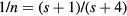 (3D case) [20] or that
  (2D case) [45]. For s = 0, these expressions reduce to the previous values of the exponent
  , obtained assuming an energy independent density of the states at the FL.
Appendix B.: Generalized Mott law
In the Mott theory [6, 7, 19], hopping conduction takes place between two sites i and j placed at distance  , whose energy separation is
  . The optimal hopping length can be obtained by maximizing the hopping probability:
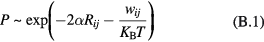
which is assumed proportional to the conductivity in a simplified picture. Here  is the inverse of the localization length
  , which is the spatial extent of the localized electronic wave function at each single site, assumed independent of energy [19]. In equation (B.1) the term
  is related to the square of the overlap integral of the electronic wave functions at the i and j sites, whereas
  is the ratio between the statistical probability of the final to initial states of the hop, given by their Boltzmann factors. At sufficiently high temperatures, when
  , the probability P is maximized by a minimum
  and the conductivity is controlled by the first factor in the exponential argument, resulting in the nearest neighboring hopping. In the opposite case (lower temperatures) or for
  , the hopping probability of equation (B.1) is maximized when the whole argument
 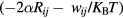 is minimum, then for hops between sites having energy within a band width
  around the Fermi energy
  (
( being the optimal energy, ±
 around
  ) and spatially separated by an average distance
  (
( called optimal length). The optimal length and the optimal band width
  are mutually related, because the number N of hops in a unitary volume must equal the number of energy exchanges in the hops, therefore also the number of energy states within the optimal band. The latter number is proportional to the density of the localized states in proximity of the Fermi energy,
  , resulting
  . By assuming a random distribution of localized sites,
  has been here calculated as
 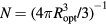 in a 3D space, and
  in a 2D space. Then, taking the conductivity proportional to the hopping probability, the following relations are obtained:
B.1. 3D case
and assuming the conductivity proportional to the hopping probability:
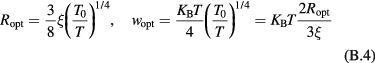
B.2. 2D case
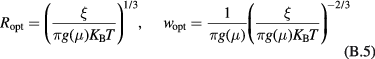
and, assuming the conductivity proportional to the hopping probability:
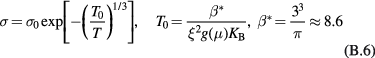
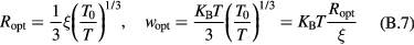
It results evident that the optimal length  and the optimal energy
  don't depend on the definition of the number N of sites in the space, provided that
  results a constant quantity; however, the details of such a definition influences the values of
  and
and  .
.
The law expressed by equation (B.1) may also be obtained by statistical considerations through the percolation theory [46, 47] for both 3D and 2D systems which lead to identical n values but slightly different  and
and  values. Namely, Ambegaokar [46] obtained
  considering a random array of localized states for a 3D system of non-interacting carriers, while Efros et al [19] obtained
  for the 2D case. Efros et al [19] obtained also
  (3D) and
  (2D) by solving a dimensionless percolation problem. These values of
  and
and  are comparable with those here deduced under simple assumptions: the differences are expected to be non-critical for the conclusions of this work. Having the aim to compare 2D and 3D density of the states at the Fermi level, we preferred to use simplified expressions for the distribution of localized sites,
  , assumed random, in order to make equal and clear hypothesis in the derivation of the formulas of equations from (B.2) to (B.7).