

Abstract
We study the magnetic properties of arrays of Co nanowires which exhibit zero bias-field ferromagnetic resonance absorptions in a 0–30 GHz range. Columnar arrays of Co nanowires with lengths of 8–15 µm were electrochemically grown using ∼20 µm thick anodic alumina membranes with 50 nm pore diameters. Microstructural, static magnetic, and microwave properties of five different nanowire arrays were characterized. The studied Co nanowires present different crystal structure textures and magnetic properties. The static magnetic loop shapes and the ferromagnetic resonance frequencies of the nanowire arrays were correctly reproduced using the Mumax3 micromagnetic software. For each sample input parameters dependent on the x-ray diffraction and microstructural data, were fine-tuned to allow the best fit of the experimental hysteresis loops and the related microwave spectra. Using this method, it was possible to analyze the rather complex interplay between geometry and magneto-structural features of the different arrays, defining which parameters play a key role in the development of nano-systems with specific microwave properties.
Export citation and abstract BibTeX RIS

Original content from this work may be used under the terms of the Creative Commons Attribution 4.0 license. Any further distribution of this work must maintain attribution to the author(s) and the title of the work, journal citation and DOI.
1. Introduction
The high-frequency behavior of conductive magnetic materials is exploited in a wide range of applications such as magnetic recording media/heads and sensors up to frequencies in the MHz range and occasionally up to the GHz range, where the permeability decreases and power losses increase, in the approach to ferromagnetic resonance (FMR). In order to increase the FMR frequency of magnetic materials, it is critical to increase the saturation magnetization and the anisotropy field. However, only very few micro- or nano-structured metallic systems possess simultaneously a high relative permeability and a high saturation magnetization (μ0 Ms > 1 T). Typical magnetic materials for high-frequency microwave applications are nonconductive Ba or Sr hexaferrite with FMR frequencies spanning from 48 GHz to 65 GHz, respectively. To date the best solution to increase the FMR frequency of metallic systems is associated with the choice of a geometry leading to large demagnetizing fields, however, this method can hardly achieve an FMR frequency higher than 10 GHz [1]. At such frequencies, the resistivity of the material becomes a critical parameter influencing the onset of eddy currents, which tend to reduce the effective sample volume and permeability. One method to avoid the detrimental effects of eddy currents is connected to the use of samples with a very small cross-section [2] arranged in an array geometry, but a generalized approach to obtain arrays of magnetic materials with nm size, high resistivity, high saturation and high anisotropy field leading to the desired microwave properties is not available yet [3–5] (expand reference list numbers).
To better identify and quantify the microstructural and magnetic parameters leading to desirable features for microwave applications also above 10 GHz, we analyzed the microstructure, static magnetic, and microwave behavior of arrays composed of polycrystalline Co nanowires with lengths of 8–15 µm ∼50 nm diameter and 105 nm inter-wire distance. The samples were electrochemically grown in a hexagonally packed configuration within anodic alumina templates under different pH conditions. The wire composition, structure, texture, and morphology were determined by x-ray diffraction (XRD) and field emission scanning electron microscopy (SEM). The static magnetic properties Mx (Hx ) with field up to H= 800 kA m−1 (1 T) applied in-plane (IP) to the anodic alumina membrane (IP, i.e. perpendicular to wire axis) and Mz (Hz ) out-of-plane (OOP, i.e. parallel to the wire axis) were measured at room temperature by a vector vibrating sample magnetometer (VSM). The nanowire arrays present a high Ms, close to the Co bulk value (∼1.8 T), and variable remanence states. Depending on the combination of microstructure and magneto-crystalline anisotropy as well as dipolar interactions [6, 7], FMR absorptions were observed in a zero applied bias field at frequencies from 2 to 32 GHz. A method is determined for the modeling of the properties through micromagnetic simulations: the static and dynamic magnetic properties of the nanowire array samples are mainly connected to the magneto-crystalline anisotropies associated with the structural texturing of the arrays, and the balance with shape anisotropy. The intent is to present a path to the analysis and simulation of the static and dynamic properties of complex magnetic nanosystems, which present non-trivial static and dynamic magnetic properties, in a fashion which can be useful for the development of microwave applications in very large frequency band range, especially in absence of external bias fields.
2. Experimental details
2.1. Sample preparation
Anodic alumina membranes with regular hexagonal nanopore arrays were prepared using a two-step process of anodization in oxalic acid [6]. The pores were subsequently widened up to a 50 nm ± 3 nm diameter using phosphoric acid and opened from both sides of the membrane by chemical etching of the alumina barrier layer and the Al substrate [7, 8]. The distance between the single nanowires corresponding to the lattice parameter of the hexagonal symmetry was maintained constant at 105 nm as determined by the oxalic bath of the anodization process. A very thin Au contact was sputtered on the bottom side as an electrode for the three-electrode deposition cell. A first electrodeposition of Au was performed to improve the electrochemical contacts. A Pt mesh and an Ag/AlCl in 4 M KCl were used as counter and reference electrodes, respectively. A potentiostatic electroplating of Co was performed on the nanoporous alumina template using an aqueous electrolyte solution containing 250 g l−1 CoSO4 and 40 g l−1 H3BO3 with a pH of 2 (samples M3-M4), pH of 6.3 (samples M40 and M8) and pH 6.5 (sample M7). The deposition was done at room temperature, under constant stirring, and at a bias voltage of −1 V (versus Ag/AgCl). A final Au layer was electroplated on top of the Co nanopillars to protect them from oxidation.
2.2. Characterization techniques
The wires length and crystal structure were characterized using a Philips XL3O scanning electron microscope and a X'Pert PRO x-ray diffractometer. An iodine solution was used prior to the XRD measurements to remove the bottom Au metallic contact layer in most of the samples. The SEM pictures were used to determine the wire length in the alumina template cross sections, while the XRD data was used to analyze the phase composition and the crystals preferential orientations present in each array. The average crystallite thickness along the wire axis was calculated through the Scherrer formula after subtraction of the instrumental contribution to the peak broadening.
Static hysteresis loops were measured for all studied samples both in the OOP configuration (Mz (Hz )), z being the wires axis, and in the IP one (My (Hy )), y being any direction in the porous alumina substrate. The measurements were performed with a VSM LakeShore Model 7310 equipped with automatic sample rotation. As the sample vibrates in the homogeneous magnetic field generated by the VSM electromagnet, its magnetic moment component projected along the applied field direction is measured by a set of pick-up coils attached to the electromagnet pole caps. In order to compare the hysteresis loops of different samples it has been necessary to normalize the magnetic moment to Ms = ±1 because of the different (and unknown) magnetic material total volume in each specimen. The magnetic field was applied between ±1 T, starting with 20 mT linear steps, using constant field with a 10 s integration time.
The FMR frequency dispersion of each of the columnar array samples was determined in field-sweep mode [10] (figure 1). The Co nanowire array membrane samples were positioned on the center of a coplanar waveguide, thus influencing the microwave circuit impedance and power transmission, which presents a higher absorption near the FMR conditions, as measured by the detector diode output voltage using a lock-in amplifier tuned to the AM modulation frequency of the microwave input. The FMR frequency dispersion was measured as a function of the OOP applied field values by positioning the CPW in the gap of an electromagnet with the center conductor perpendicular to the applied field direction. The experimental results obtained were composed of sets of voltage curves proportional to the power absorption, plotted as a function of the applied field measured between f = 1 GHz and 40 GHz at 1 GHz intervals with −10 dBm or 0 dBm input power and with a DC applied field varying between μ0 Hz = ± 1.3 T in 5 mT steps. Absorption peaks at one or more values of the applied field were identified within the set of measured frequencies (see figure 1(bottom)).
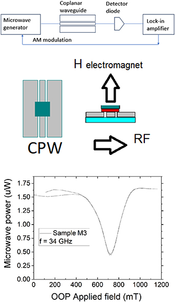
Figure 1. (Top) FMR measurement experimental setup and (Middle) coplanar waveguide (CPW) with sample scheme. The porous alumina is placed with the sample face on the CPW surface. The H direction corresponds to an out-of-plane static Hz field, while the microwave field (RF) produced by the waveguide interacts with the sample. (Bottom) Experimental FMR Peak example, sample M3 microwave source set at 34 GHz, absorption peak observed with scanning applied field μ0 Hz = 700 mT as voltage on the detector diode output.
Download figure:
Standard image High-resolution image3. Micromagnetic modeling
A set of micromagnetic simulations was performed using the mumax3 package [11] on Linux computers equipped with NVIDIA GeForce GTX 1070 8 GByte (minimum requirement) or NVIDIA Quadro RTX 6000 card 24 GByte GPU graphic cards. With a choice of input parameters based on the magnetic and microstructural data extracted from the experimental characterization (see tables 1(a) and (b)—to be discussed in the next section).
Table 1. (a) Deposition and XRD microstructural data summary. (b) Experimental magnetic summary, VSM and FMR data.
| (a) | |||||
| Sample ID | M3 | M4 | M7 | M8 | M40 |
| Electrolyte pH | 2 | 2 | 6.5 | 6.3 | 6.3 |
| Wire length (μm) | 12 | 8 | 15 | 13 | 12 |
| Crystal structure | fcc | fcc | hcp | hcp | hcp |
| Main XRD peaks | 220 | 220 | 002, 100 | 101, 100 | 201, 101, 100 |
| Grain size (crystallite thickness along wire axis) (nm) | 136 | 120 | 31 | 8 | 22 |
| (b) | |||||
| Sample ID | M3 | M4 | M7 | M8 | M40 |
| Remanence Mzr /Ms | 0.48 | 0.1 | 0.28 | 0.26 | 0.35 |
| Coercivity Hzc (mT) | 160 | 91 | 90 | 90 | 100 |
| Remanence Myr /Ms | 0 | 0 | 0.02 | 0.12 | 0.23 |
| Coercivity Hyc (mT) | 0 | 0 | 0.03 | 5 | 45 |
| H = 0 FMR (GHz) | 20 | 2 | 7; 19 | 12; 32 | 5; 12 |
Mumax3 calculates the magnetization dynamics solving numerically the LLG equation:

where  is the normalized local magnetization,
  is the effective field, α is the damping constant and γ0 is the gyromagnetic factor. The effective field
  contains all the contributions to the magnetic energy, which in our system include the external field, the exchange energy, the magnetostatic (or dipolar) field and the magnetocrystalline anisotropy. The effective field then becomes
where  is the external field,
  the exchange constant,
  the anisotropy constant and
  the uniaxial anisotropy easy axes.
  and
and  are different for each texture analyzed.
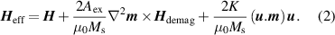
In the calculations of the magnetostatic field  and the exchange field, Mumax3 has the possibility to include periodic boundary conditions (PBCs), through the SetPBC(int, int, int) function, which sets the number of repetitions in X,Y,Z to create PBCs. PBC(X,Y,Z) applies PBC conditions in the (x,y,z) axis if the corresponding (X,Y,Z) index is different from zero. PBC(0,0,Z) means that the contribution to the dipolar field, which depends on sample geometry, includes Z copies of the base system in each z direction (Z copies on the top and Z copies on the bottom of the base volume). For example PBC(0,1,0) with X = 0, Y = 1, and Z = 0 means that the base (x,y,z) system composed of 13 wires shown in figure 2(a), becomes a system of 39 = 13(2Y + 1) wires shown in figure 2(b), with a of total height z (given in table 2(b)).
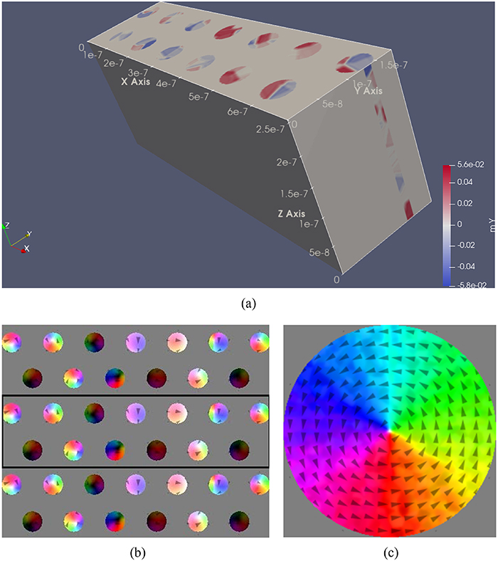
Figure 2. (a) Simulations: depiction of the base volume of 13 wires (axes size m) used for the simulation (the edges of the vertical wires are visible on the top surface of the volume, where the red and blue colors correspond to the my component of magnetization at the start of a simulation). Figure made with the ParaView application [9]. (b) Simulations: top view (x,y) of the full ensemble of 39 wires being simulated. The black lines outline the base system also depicted in figure (a). Here we show the extension along the y direction (vertical) using the periodic boundary conditions PBC (0,1,0). The figure shows a remanence magnetization state. Different colors represent different magnetization directions, color map in figure (c). (c) Simulations: color map vs magnetization direction (arrows).
Download figure:
Standard image High-resolution imageTable 2. (a) Mumax3 input parameters used: microstructure and anisotropy. (b) Mumax3 input parameters used to fit the static magnetic properties: OOP and IP hysteresis loops -coercive fields Hzc, Hxc and approach to saturation. (c) Post-processing fitting of OOP and IP loop slope equation (1) and position of FMR peaks.
| (a) | |||||
| Sample ID | M3 | M4 | M7 | M8 | M40 |
| Anisotropy type | fcc | fcc | hcp | hcp | hcp |
| Main peaks and relative weight (%) | 220 (100) | 220 (100) | 002 (99), 100 (1) | 101 (80), 100 (20) | 201 (45), 101 (45), 100 (10) |
| Angles of the anisotropy axes w.r.t the wire axis | 90°, 45° | 90°, 45° | 0°, 90° | 62°, 90° | 75°, 62°, 90° |
| Crystallite thickness (nm) | 136 | 120 | 31 | 8 | 22 |
| Anisotropy (J m3) | 25 × 104 | 25 × 104 | 45 × 104 | 45 × 104 | 45 × 104 |
| 4 × 10⁴ | 4 × 10⁴ | ||||
| (b) | |||||
| Sample ID | M3 | M4 | M7 | M8 | M40 |
| Simulated volume z height (nm) | 256 | 550 | 28 | 256 | 256 |
| PBC | (011) | (011) | (010) | (018) | (018) |
| Total z height including PBC (μm) | 0.77 | 1.65 | 0.028 | 2.304 | 2.304 |
| (c) | |||||
| Co NW Sample ID | M3 | M4 | M7 | M8 | M40 |
| Ndz OOP | 0.1 | 0.5 | 0.2 | 0.2 | 0.05 |
| Ndx IP | 0.04 | −0.13 | 0.22 | −0.06 | −0.1 |
To include the distribution of properties given by the grain structure, we also included a distribution of Voronoi grains with a given average size shown in table 1(a) [12]. The sample is divided in grains and the exchange interaction in the boundary of the grains has a reduced value of Ascale. The value of the anisotropy constant has a random contribution for each grain, which is described in the parameter section table 2(a).
To execute the simulations within the available memory size and with acceptable execution times, the hexagonal geometry of the nanowire arrays was modelled using for all samples a set of 13 cylindrical wires of 50 nm diameter arranged in 2 rows (6 and 7 wires each) see figure 2(a) with a 105 nm interwire distance. A mesh of 1.6 nm × 1.6 nm × 1.6 nm was used for a total simulation volume of 630 nm (105 × 6 + 50 nm) by 260 nm (105 + 50 + 105 nm) by wire height. Each sample required using a specific wire height z for the simulation, ranging from 28 nm to 550 nm. As mentioned above, the PBC function (PBC) of mumax3 was used PBC(0, 1, Z) for all samples so that an approximately square (x, y) lattice of 39 wires was obtained (see figure 2(b)), while in the z direction Z values from 0 to 8 were used as discussed in the following. Simulations were repeated modifying either the simulated wire height and PBC or the volume ratio between different crystalline textures to achieve a correct shape of the hysteresis loops (see experimental data in table 1(b)).
Table 2(a), reports the mumax3 input parameters used, which could be directly derived from the experimental data reported in table 1(a), complemented by literature values of anisotropy constants [13–16]. For each sample, the crystal structure, textures, and the direction of the anisotropy axes with respect to the wire axis, were identified from the peak intensities in the XRD patterns (see table 2(a) for values). Azimuthal orientation was randomly selected.
It should be noted that all the values of the parameters connected to experimental data as shown in table 2(a) were kept fixed during all the different simulations.
Table 2(b) shows the simulation parameters used in this work, which could not be derived directly from experimental data, namely the wire height and Z value of PBC(0,1,Z). The simulated wire height balances the equilibrium between the shape and magneto-crystalline anisotropies and contributes to defining the coercive field of the hysteresis loops. The length values were chosen to obtain an agreement between experimental and simulated loop shape. The choice of small height values in the simulations can be connected to several causes such as reduced grain size, discontinuities in the wire growth and presence of structural defects which reduce the magnetic correlation length of the polycrystalline wires within the nanopores of the alumina matrix.
Once the static loops were simulated, the same parameters were used to compute the microwave spectra of each sample. A static bias field was applied along the z-axis with values ranging from 0 to ∼1 T, and a pulsed field was applied along the y-axis, using a cardinal function sinc(t) = sin(t)/t; t = 1 ps. The oscillations of My (t) were computed and recorded for a total of 2 ns in 1 ps time steps. Finally, the My (t) time domain signal was post-processed using the mumax3-fft package to obtain the frequency domain response of the sample to the pulse.
These simulated FMR spectra were analyzed in the frequency-domain and compared with the experimental absorption. As a final step, due to the reduced number of wires simulated (39), as compared to the ∼4 × 10⁸ wires in a real sample, it was useful to include a demagnetizing coefficient Nd due to macroscopic dipolar fields which cannot be taken into account in such a small ensemble of wires, and obtaining the final magnetization vs bias field relation:

used during the post-processing of the data to correct the simulated static loop shapes as well as the FMR frequency vs field FFMR(Hz ) dependence.
4. Results and discussion
Five samples were considered, presenting an interesting range of different textural, magnetic, and microwave properties: M3, M4, M7, M8, and M40. These samples have different lengths, crystal structure and preferential orientation of the crystals.
Figure 3(a) displays the XRD patterns of selected samples of nanowires embedded into the templates. As previously reported [15] the NW crystal structure was found to be highly sensitive to the electrolyte pH during deposition: the samples deposited from a low-pH bath (M3 and M4) are composed of face-centered-cubic (fcc) Co, while the samples deposited at pH close to neutrality (M7, M8 and M40) develop a hexagonal-close-packed (hcp) structure. Besides, the deposition conditions influence the preferential orientation of the crystals with respect to the nanowire axis, as deduced by the relative intensities of the XRD peaks, compared to the ones expected for a randomly oriented powder. Fcc samples are highly textured, with {110} planes perpendicular to the wire axis, whereas, among the hcp samples, only M7 has a very strong [002] texture, indicating the predominance of crystals with their c-axis almost parallel to the wire axis. XRD patterns of M8 and M40 samples, instead display a more complex coexistence of reflections, in relative intensities anyway different from the random powder. The average crystallite thickness along the wire axis was also very different among the samples and was found to be in the range from about 8 nm to about 136 nm.
Figure 3. (a) XRD patterns and SEM pictures of the samples. M4 spectra not shown, due to similarity with M3. (b) Sketches of the crystal orientation with respect to the nanowire axis for fcc and hcp crystals with different preferential orientations: the angles between the wire axis and the anisotropy axes are displayed in red. Drawings of the crystal cells have been produced with Vesta 3 software [17].
Download figure:
Standard image High-resolution imageThe results of the micromagnetic simulations of each sample are summarized in the following subsections together with a discussion of the parameters used for the simulations of the OOP and IP magnetization curves as well as the FMR microwave behavior.
The mumax3 parameters used, common to all samples were: mesh (cx,cy,cz) = 1.6 nm; wire diameter 50 nm; interwire center-to-center spacing 105 nm; exchange coupling Aex = 15.4 × 10⁻¹² J m−1; exchange coupling at the grain boundary Ascale = 0.9Aex; saturation magnetization Ms= 1.360 × 10⁶ A m−1; damping constant α = 0.05; h.c.p. anisotropy constant Ku = 4.5 × 10⁵J m−3; f.c.c. anisotropy constants K1 = 2.5 × 10⁵ J m−3 and random fluctuations K1std = 5 × 10⁴J m−3 (at 90° to the wire axis) and K2 = 4 × 10⁴ J m−3 and K2std= 1 × 10⁴J m−3 (at 45° to the wire axis).
5. Sample details
M3 sample
The Co nanowire sample M3 grown under pH 2 is composed of 12 μm long wires, as measured through SEM imaging. The magnetic OOP loop measured by VSM Mz (Hz ) is composed of quasi-linear branches near the μ0 Hzc = 160 mT coercivity (figure 4). The OOP remanence Mzr ∼ 0.48 (normalized to Ms= 1) shows that the zero-field magnetization is quite strongly directed along the wire axis due to the shape anisotropy. The XRD pattern shows a single sharp (220) peak of fcc Co (figure 3(a)); an average crystallite thickness of 136 nm along z can be estimated from peak width. 100% of the magnetic volume iscrystal structure with one easy axis at 45° and another one at 90° to the wire axis (i.e. the <100> directions) figure 3(b). The IP loop curve Mx (Hx ), perpendicular to the wire axis, also has a linear dependence on the field and an almost zero Hxc coercivity and zero Mxr remanence, a telltale sign of IP magnetization processes mainly due to rotations with very small hysteresis. In summary, the experimental data collected indicates that the shape anisotropy and the crystalline anisotropy at 45° to the wire axis tend to prevail, as confirmed by the FMR spectra showing a quite high zero-field FMR absorption which can be extrapolated from experimental data at 20 GHz.
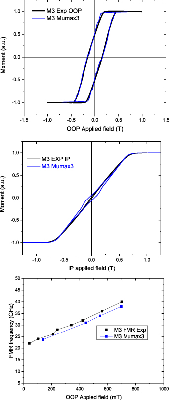
Figure 4. Experimental (black) and simulated (blue) magnetization curves of sample M3: (top) OOP Mz (Hz ) loops, (center) IP Mx (Hx ) loops, (bottom) FMR absorption peaks as a function of the OOP Hz applied field.
Download figure:
Standard image High-resolution imageM3 sample simulation parameters
The simulations results shown in figure 4 show that a good fit of the experimental Mz (Hz ), Mx (Hx ) magnetic hysteresis loops and FMR absorption spectra can be obtained under the assumption of a sample height of 256 nm and a PBC(0,1,1). The simulation parameters indicate that shape anisotropy and magneto-crystalline anisotropy produce an overall anisotropy directed along the wire axis. In order to obtain this effect in a cubic anisotropy sample, where the prevailing magnetocrystalline anisotropy is at 90° to the wire axis, a 256 nm length was used coupled to a PBC(110) which brings the effective wire height used to 770 nm. This value is much smaller than the total wire length of 12 μm determined experimentally, but it was required to obtain the correct OOP and IP coercivity and magnetization curve. The shape anisotropy of a cylinder 770 nm long and 50 nm diameter results directed along the wire axis, even when combined with a cubic anisotropy of the f.c.c. (220) texture, which has the main component directed at 90° to the wire axis and the second one at 45°. The anisotropy values associated with each crystalline grain in the 39 wires were randomly extracted according to a uniform distribution with value K1, and with random fluctuations K1std.
K1 = 2.5 × 10⁵J m−3, K1std= 5 × 10⁴J m−3 (at 90° to the wire axis) and K2 = 4 × 10⁴J m−3 and K2std= 1 × 10⁴J m−3 (at 45° to the wire axis). These values were chosen using the available literature data to reproduce the magnetic behavior of the array [13–16]. An additional demagnetizing coefficient Ndz = 0.1 for HZ (Mz ) and Ndx = −0.001 for HX (Mx ) was used to modify the loop slopes, reducing the permeability near the coercive point and also correctly shifting the FMR frequency vs field fFMR(Hz ) dependence to higher applied fields. An f = 20 GHz FMR absorption mode was found, under a zero bias field. Correct IP and OOP loops, and FMR behavior were computed.
M4 sample
The Co nanowire sample M4, also grown under pH 2, is composed of 8 μm long wires. The XRD data (not shown) are very similar to the previous case, displaying a single sharp fcc (220) peak with crystallites of average thickness of 120 nm (along z), 10% smaller than M3. The magnetic OOP loop Mz (Hz ) is composed of quasi-linear branches with μ0 Hzc = 91 mT coercivity, which is much smaller than case M3 (figure 5). The OOP remanence Mzr ∼ 0.16 (normalized to Ms= 1) shows that the zero-field magnetization is only feebly directed along the wire axis and compatible with the fcc (220) preferential orientation, i.e. easy directions along the edges of the cubes, either perpendicular to the wire axis, or at 45° to it. The IP loop curve Mx (Hx ), with Hx perpendicular to the wire axis, also has a linear dependence on the field and an almost zero Hxc coercivity and zero Mxr remanence, again a sign of magnetization processes mainly due to rotations with almost no connected hysteresis losses. In summary, the experimental data collected indicate that the cubic anisotropy and dipolar interactions for sample M4 lead to a magnetic behavior that is quite isotropic in spite of the nanowire geometry, and the zero bias FMR frequency can be extrapolated to a small value of 2 GHz.
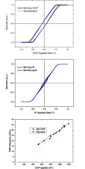
Figure 5. Experimental (black) and simulated (blue) magnetization curves of sample M4: (top) OOP Mz (Hz ) loops, (middle) IP Mx (Hx ) loops, (bottom) FMR absorption peaks.
Download figure:
Standard image High-resolution imageM4 sample simulation parameters
A fit of the Mz (Hz ), Mx (Hx ), and FMR absorption spectra experimental results of figure 4 were obtained under the assumption that the whole sample (100%) is composed of grains with a (220) f.c.c. texture with crystallites of 120 nm dimension (along z) and a simulated volume length of 512 nm with PBC(0,1,1), bringing the effective wire height used to 1550 nm, twice the previous sample M3, and such that the combination of simulated wire geometry and cubic anisotropy leads to the correct modeling of the macroscopic wire behavior, quite isotropic in the OOP and IP directions. The anisotropy values of each nanocrystal were randomly extracted according to a uniform distribution with value K1, and with random fluctuations K1std. K1 = 2.5 × 10⁵J m−3 K1std = 5 × 10⁴J m−3 (at 90° to the wire axis) and K2 = 4 × 10⁴J m−3 and K2std = 1 × 10⁴J m−3 (at 45° to the wire axis). One main FMR absorption mode with a zero bias-field frequency of 2 GHz was observed (extrapolated from data at higher fields) and correctly simulated using the same structural parameters. The additional demagnetizing coefficients Ndz = 0.48 for Hz (Mz ) and Ndx = −0.2 for HX (Mx ) were needed to obtain the correct loop slopes and also to obtain the correct FMR frequency vs field fFMR(Hz ).
The main difference between the M3 and M4 samples, which share the same crystalline structure and anisotropy constants, from the point of view of loop shape and FMR frequency, is only associated with the lengths required to correctly simulate the loops, which for sample M3 with a PBC(0,1,1) is 256 nm*(2 + 1) = 768 nm while for sample M4 also with a PBC(0,1,1) is 550 nm *(2*1 + 1) = 1650 nm. It is then evident that, in the case of fcc wires, shorter wires may be more easily magnetized OOP along the wire axis.
M7 sample
Sample M7 is composed of very long 15 μm wires, grown under a pH of 6.5, which promotes the growth of a hcp. structure, here found with a main (002) texture, accompanied by one additional (100) smaller peak (see figure 6). An average crystallite thickness of 31 nm along z was estimated by the (002) peak width. The strong [002] preferred orientation implies a magnetocrystalline anisotropy pointing along the wire axis for most of the grains, while the residual crystals giving rise to the (100) reflection, have their anisotropy axis perpendicular to it. The result of this competition of wire shape and texture is a magnetic OOP loop Mz (HZ ) composed by almost linear branches near the μ0 Hzc = 9 mT coercivity and a remanence Mzr = 0.28 Ms indicating a partial magnetization along the wire axis in absence of external field. The IP loop curve Mx (HX ), has a sigmoidal shape and presents a very small remanence Mxr = 0.02 Ms and hysteresis μ0 Hxc = 0.03 mT, connected to a prevalence of magnetization by rotation under IP applied field. The FMR shows two zero-bias absorption peaks at about 7 GHz and 20 GHz also due to the two present textures.

Figure 6. Experimental (black) and simulated (blue) magnetization curves of sample M7: (left) OOP Mz (Hz ) loops, (center) IP Mx (Hx ) loops, (right) FMR absorption peaks as a function of the OOP Hz applied field.
Download figure:
Standard image High-resolution imageM7 sample simulation parameters
A fit of the static and microwave behavior was obtained assuming the superposition of two different uniaxial anisotropy components, one associated to the (002) texture, and the other the (100) texture, the first occupying 95% of the total volume. Two crystalline anisotropy directions were used in association with the two textures. Polar angles either 0° or 90° and random azimuthal angles values for each nanograin of 28 nm occupying the whole sample length were extracted according to a uniform distribution with value K= 45 × 104 J m−3 with random fluctuations Kstd= 5 × 10⁴ J m−3 for both cases (crystals' c-axis at 0° and at 90° to the wire axis).
An additional demagnetizing coefficient was applied Ndz = 0.2 for Hz (Mz ) and Ndx = −0.22 for Hx (Mx ) to obtain the correct loop slopes and also to obtain the correct FMR frequency vs field fFMR(Hz ) dependence. Two main FMR absorption modes were found through dynamic simulations, closely resembling the experimentally observed ones. A very specific small grain/small length condition with a PBC(0,1,0) was required in order to obtain the rather reduced anisotropy along the wire axis compatible with the experimentally observed OOP Hc field and the microstructure found by XRD.
M8 sample
Sample M8 was composed of 13 μm long wires grown under a pH of 6.5, also showing a hcp crystal structure, but with a less developed texture than the previous cases: the main (101) peak, expected to be the main reflection in a random powder, is accompanied by an almost equally intense (100) reflection and by minor (002), (110) and (201) peaks. Very small crystallites of 8 nm thickness were found. The (101) reflection represents crystals oriented in such a way that their anisotropy axis is at 62° to the wire axis, while, in the case of the (100)reflection, the c-axis of the corresponding crystals is perpendicular to the wire axis. The result of this competition of wire shape and different textures is a magnetic OOP loop Mz (Hz ) composed by almost linear branches near the μ0 Hzc = 9 mT coercivity and a remanence Mzr = 0.26 Ms (figure 7). The IP loop curve Mx (Hx ), has a sigmoidal shape and a peculiar central constriction which reduces the coercivity to just μ0 Hxc = 5 mT while the remanence is quite significant Mr =0.12 Ms. The central constriction can be connected to a mixture of harder and softer magnetic textures which cause an evident IP hysteretic behavior, usually associated to magnetization through domain wall motions, while magnetization rotations with no associated hysteresis are prevalent at high IP field. The resulting FMR behavior was more complex than the previous samples, presenting two zero-bias absorption peaks at 12 and 33 GHz and a third mode appearing at low frequency with a bias field μ0 Hz = 0.5 T.

Figure 7. Experimental (black) and simulated (blue) magnetization curves of sample M8: (top) OOP Mz (Hz ) loops, (center) IP Mx (Hx ) loops, (bottom) FMR absorption peaks as a function of the OOP Hz applied field.
Download figure:
Standard image High-resolution imageM8 sample simulation parameters
A fit of the rather complex static and microwave behavior, shown in figure 6, was obtained assuming the superposition shape anisotropy with two different crystalline anisotropy components the (101) occupying 80% of the volume while the remaining 20% is (100) directed at 90° to the wire axis. The anisotropy values of each nanograin were extracted according to a uniform distribution with value K= 45 × 104 J m3 with random fluctuations Kstd= 5 × 10⁴ J m3 with polar angles as defined above and random azimuthal angles. A total z wire height of 256 nm with a PBC(0,1,8) for a total of 2304 nm was simulated. An additional demagnetizing coefficient due to size-related dipolar field was applied.
Nd= 0.3 for Hz (Mz ) and Nd= −0.11 for Hx (Mx ) to obtain the correct loop slopes and also to obtain the correct FMR frequency vs field FFMR(Hz ) dependence. Three FMR absorption modes were found through dynamic simulations, closely resembling the experimentally observed ones, with zero field absorptions at about 12 GHz and 32 GHz, and one additional transversal mode found with an applied field μ0 Hz > 500 mT.
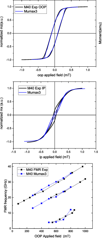
M40 sample
Sample M40, 12 μm long and electrochemically grown with a pH 6.3 presents three reflections of hcp Co in the XRD pattern: the distinctive feature is a (201) peak highly enhanced in intensity, which is associated to crystals with c-axis at 75° to the wire axis, accompanied by a (101) and (100) reflections representing crystals with c-axis at 62° and at 90° to the wire axis, respectively (see figure 3(b)). The result of the superposition of the wire array geometry and the different textures is a magnetic OOP loop Mz (Hz ) loop with almost linear branches near the μ0 Hzc = 100 mT coercivity and normalized remanence Mzr = 0.35 Ms (figure 8). The IP loop curve Mx (Hx ), has a sigmoidal shape and an evident hysteresis associated to the anisotropy directed perpendicularly to the wire axis, with a coercivity μ0 Hxc = 50 mT and a remanence Mxr = 0.23 Ms, while magnetization rotations and no associated hysteresis prevail at high IP fields. The FMR absorption behavior shown in figure 6 also shows 3 main modes with two zero bias absorption peaks at 5 and 12 GHz and a third transversal mode appearing with a bias μ0 Hz > 400 mT.
Figure 8. Experimental (black) and simulated (blue) magnetization curves of sample M40: (top) OOP Mz (Hz ) loops, (center) IP Mx (Hx ) loops, (bottom) FMR absorption peaks.
Download figure:
Standard image High-resolution image
M40 sample simulation parameters
A fit of the static and microwave behavior of sample M40 was obtained assuming the superposition of three anisotropy distributions connected to the three to the different structural textures found by XRD (201), (101) and (100). We assume that the volume fractions of 45% is occupied by the '(201) oriented' crystals, 45% by the '(101) oriented' and 10% by (100) components. A sample z height of 256 nm and PBC(0,1,8) for a total of 2304 nm was used with median z crystallite thickness of 22 nm.
An additional demagnetizing coefficient due to size-related dipolar field was applied Nd= 0.2 for Hz (Mz ) and Nd = −0.1 for Hx (Mx ) to obtain the correct loop slopes and also the FMR frequency vs field FFMR(Hz ) dependence. Three FMR absorption modes were found in the dynamic simulations, which correctly fit the experimental ones.
6. Conclusions
In order to obtain magnetic wire arrays with nm dimensions, high resistivity, high saturation and high anisotropy field leading to desirable microwave properties, we have electrochemically deposited Co nanowire arrays of different lengths, crystal structure and textures. Their static and dynamic magnetic properties assessed with conventional experimental techniques (VSM, FMR) revealed substantial differences among the samples. However, using the mumax3 micromagnetic simulation package, and using the experimental quantities determined as main reference for the definition of the simulation parameters we were able reproduce the static and dynamic behavior of the samples.
The analysis shows that the correct identification of the crystalline structure and texture and their magnetic anisotropies, as well as the magnetically-active size of the sample, connected to the shape anisotropy, allows to correctly predict the static magnetic properties as well as the microwave absorptions. This work shows a possible path to the analysis and simulation of the static and dynamic properties of rather complex magnetic nanosystems, which present non-trivial static and dynamic magnetic properties also for the development of specific wideband microwave applications in zero applied bias field conditions. Here it was possible to observe and correctly simulate FMR absorptions at frequencies ranging from 2 to 32 GHz.
Acknowledgments
This work has been partially performed at NanoFacility Piemonte, an INRiM laboratory supported by Compagnia di San Paolo Foundation. We also acknowledge the support of the Regional Government of Madrid under Project S2018/NMT-4321 NANOMAGCOST-CM.
Data availability statement
All data that support the findings of this study are included within the article (and any supplementary files).