
Abstract
Monolithic integration of III–V optoelectronic devices on Si platform is gaining momentum, since it enables advantages of low cost, less complexity and high yield for mass production. With the aim of achieving advances in monolithic integration, the challenges associated with lattice mismatch between III–V layers and Si substrates must be overcome, as a low density of threading dislocations (TDs) is a prerequisite for the robustness of the integrated devices. In this paper, we have investigated and compare different types of dislocation filter layers (DFLs) from InGaAs asymmetric step-graded buffer layer (ASG), InGaAs/GaAs strained-layer superlattices, and quaternary alloy InAlGaAs ASG, on the functionality of reducing TD density (TDD) for GaAs buffer layers on Si. Compared to other DFLs, the sample with InAlGaAs ASG buffer layer shows the lowest average TDD value and roughness, while the decrease of TDD in the sample with InAlGaAs ASG buffer layer can be understood in terms of the hardening agent role of aluminium in the InAlGaAs ASG. By further optimising the InAlGaAs ASG through thermal cyclic annealing, we successfully demonstrate a low surface TDD of 6.3 ± 0.1 × 106 cm−2 for a 2 μm GaAs/InAlGaAs ASG buffer layer grown on Si. These results could provide a thin buffer design for monolithic integration of various III–V devices on Si substrates.
Export citation and abstract BibTeX RIS

Original content from this work may be used under the terms of the Creative Commons Attribution 4.0 license. Any further distribution of this work must maintain attribution to the author(s) and the title of the work, journal citation and DOI.
1. Introduction
High-performance semiconductor lasers integrated on a Si platform have attracted great interests for realising Si-based photonic integrated circuits (PICs), owing to the potential properties of low cost, high bandwidth and high integration level. However, due to the nature of the indirect bandgap of Group-IV bulk material, the performance of Group-IV lasers, including the stimulated Si Raman laser, rare-earth-doped laser, and n-type doped germanium laser, is scarcely sufficient for practical application and cannot compete with the performance of III–V lasers [1, 2]. Until now, the mainstream commercialised Si-based PICs are based on hybrid integration and heterogeneous integration [3, 4]. However, both approaches suffer from the high complexity and the high cost of mass production [5]. Extensive studies have thus been instigated by researchers worldwidely on the epitaxial growth of III–V materials on Si substrates to achieve a more cost-efficient method for high-yield III–V materials on Si (III–V/Si) lasers. However, the intrinsic contrasting characteristics between the III–V and Si materials, including large lattice mismatch, incompatible thermal expansion coefficients, and different symmetry crystal structures lead to the formation of various crystallographic defects, including threading dislocations (TDs), thermal cracks and anti-phase boundaries (APBs) [6–11]. These crystallographic defects can propagate into the active region and act as non-radiative recombination centres, hence greatly hindering the laser performance in terms of operating power and temperature, output efficiency and device reliability [10–12].
Recently, Li et al and Rio Calvo et al have successfully developed new practices to achieve the self-annihilation of APB for GaAs and GaSb epitaxial growth on the nominal on-axis Si (001) substrates, respectively [13, 14]. However, the inevitable high density of TDs coming from a 4% lattice mismatch between GaAs and Si prompts continued interest in reducing the TD density (TDD) in GaAs buffer layers. Various approaches have been studied in specific defined directions, where the strained-layer superlattices (SLSs) and graded buffer layer are the primary methods for reducing the TDD, along with high temperature annealing processes [15–17]. The InAlAs/GaAs SLSs and the InGaAs asymmetric step-graded filter (ASG) all demonstrated effectiveness in reducing the density of TDs and have been able to reach the level of ∼106 cm−2 previously [7, 16, 17].
In this paper, a new dislocation filter layer (DFL), InAlGaAs ASG, has been developed to reduce the TDD in GaAs buffer structure grown on Si substrates. The density of TDs is efficiently reduced to 6.3 × 106 cm−2, which is better than the TDD in samples grown under the same conditions with InGaAs SAG and InGaAs/GaAs SLSs. These results suggest that the sample with quaternary InAlGaAs ASG is a promising DFL for all kinds of arsenic materials epitaxially grown on Si substrates for various applications.
2. Experiments
All samples were grown on n-type Si (100) substrates by using a Veeco Gen-930 solid-source molecular beam epitaxy system. In-situ deoxidisation of the Si substrate was accomplished by holding the substrate at 950 °C for 10 min before the material growth. The substrates were then cooled down to 375 °C for the growth of a 5 nm AlAs nucleation layer via migration-enhanced epitaxy, followed by a subsequent 1.35 μm GaAs buffer with an optimised three-step growth scheme [18]. Thermal cyclic annealing (TCA) was then performed from 320 °C to 680 °C with a hold time of 7 min for eight iterations with arsenic overpressure to protect the epi-surface. As the thermal expansion coefficient of GaAs is distinctly larger than the Si, each single thermal annealing procedure will generate ∼140 MPa of biaxial stress (according to the COMSOL Multiphysics simulation result). The kinetic constraints are substantial in the TD reducing strategy as the glide of glissile dislocations is thermally activated. TCA enables glissile TDs to have larger possibilities to meet and annihilate when gliding on the same plane [16, 19, 20]. The annealing temperature for the GaAs layer is designed to maximise the kinetic energy of the dislocation while keeping the quality of the crystal; the highest temperature is set according to the brightness of the pattern on the reflection high energy electron diffraction (RHEED) monitor, and the substrate was gradually heated up with the step of 10 °C min−1 until the brightness of the RHEED pattern gets dark. After the TCA process, three different types of DFL are grown, including InAlGaAs ASG, InGaAs ASG and InGaAs/GaAs SLSs. Figure 1(a) shows the InAlGaAs ASG structure consists of a 150 nm In0.05Al0.35Ga0.6As, a 200 nm In0.1Al0.7Ga0.2As and a 300 nm In0.05Al0.35Ga0.6As, while the growth temperature was curtailed to 470 °C to avert the phase separation concern for the InAlGaAs quaternary alloy [21, 22]. The ASG structure was finally capped with 300 nm GaAs on the top. The other two samples were grown under identical conditions but with the InGaAs/GaAs SLSs DFL and InGaAs ASG structure replaced. As shown in figure 1(b), the InGaAs/GaAs SLSs structure consists of two sets of In0.2Ga0.8As/GaAs SLSs, where each set of SLSs has five iterations of 10 nm In0.2Ga0.8As, 10 nm GaAs and a 350 nm GaAs spacer layer. To keep all DFL structures are in same thickness, so the GaAs buffer layer in the InGaAs/GaAs SLSs structure is increased to 1.4 μm. Figure 1(c) presents the InGaAs ASG DFL which consists of a 150 nm In0.05Ga0.95As, a 200 nm In0.1Ga0.9As, and a 300 nm In0.05Ga0.95As respectively. In this work, the samples were studied by electron channelling contrast imaging (ECCI), Raman spectroscopy, atomic force microscopy (AFM), high-resolution x-ray diffraction (HRXRD) (004) symmetrical scan, reciprocal space maps (RSMs) around the (224) lattice plane and transmission electron microscopy (TEM). The ECCI images were taken by Zeiss XB1540 crossbeam scanning electron microscope equipped with backscattered electron detector to determine the TDD of the samples without destroying the sample surface. The AFM images were taken by using Brucker ICON system by using tapping mode, while the AFM tips has a maximum radius of 7 nm. X-ray diffraction (XRD) measurements were performed at room temperature with a Jordan Valley Bede D1 x-ray diffractometer equipped with a Cu Kα source and detected by a YAP:Ce scintillator. The intervals of RSM are set to 0.2° with a step size of 0.02°. Raman spectroscopy was studied by using a Renishaw inVia InSpect Raman microscope equipped with a 532 nm excitation laser at room temperature, the spectral range was 100–600 cm−1. The surface morphology was observed by a Bruker Dimension Icon AFM in tapping mode.
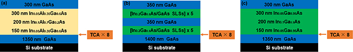
Figure 1. Schematic structure diagrams showing the buffer layer structure with (a) InAlGaAs ASG, (b) InGaAs/GaAs SLSs, and (c) InGaAs ASG respectively. The entire buffer thickness of these three structures is kept identical at 2.3 μm.
Download figure:
Standard image High-resolution image3. Results and discussion
The effects of TCA and different DFLs on the TDD within GaAs buffer layers grown on Si were first studied by ECCI. Figure 2(a) shows the surface of the original unoptimised 1.4 μm GaAs buffer grown on Si substrate with a TDD of ∼109 cm−2, which is reduced to the level of 1.21 × 108 cm−2, as shown in figure 2(b) after being subjected to a common practice of TCA process before growing the DFLs [23, 24]. The representative surface ECCI images of InAlGaAs ASG, InGaAs/GaAs SLSs, and InGaAs ASG are shown in figures 2(c)–(e), respectively, where all the TDs are marked by red hollow circles. Figure 2(f) presents the trend of the counted TDD before the DFL and after three different types of DFL, which shows a significant decrease in TDD by using all three DFLs. For each sample, the TDD is averaged from seven scanning images of each size of 306 μm2, giving a total scanning area size of 2142 μm2, so that the results are representative while ensuring that the TDs are still noticeable in the image. The lowest overall TDD is achieved by the sample with InAlGaAs ASG showing a value of 6.5 × 106 cm−2, proving that the InAlGaAs ASG is the most effective structure to reduce the TDD.
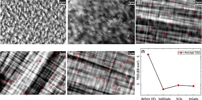
Figure 2. (a) The ECCI of 1.4 μm GaAs directly grown on Si substrate; (b) the ECCI image of 1.4 μm GaAs directly grown on Si substrate after eight iteration of TCA treatment; the representative surface ECCI image of (c) InAlGaAs ASG structure; (d) InGaAs/GaAs SLSs structure; and (e) InGaAs ASG structure respectively. (f) The average counting of TDD before and after different threading dislocation reduction structures.
Download figure:
Standard image High-resolution imageXRD measurements were further utilised to investigate the discrepancies in the crystal quality of GaAs and to elucidate the degree of stress relaxation inside the different DFL structures. Figure 3(a) shows HRXRD omega-2theta scans over symmetric (004) reflection for these three samples which indicates the peaks of GaAs and Si. Both In0.05Ga0.95As/In0.1Ga0.9As and In0.05Al0.35Ga0.6As/ In0.1Al0.6Ga0.3As peaks are observed clearly. In contrast, the satellite peaks indicate the In0.2Ga0.8As/GaAs SLSs with a period of thickness of around 20 nm (10 nm InGaAs and 10 nm GaAs). To investigate the efficiency of different TDD reduction strategies further, the RSM scans around (224) are taken. RSM scans in figures 3(b)–(d) were created by taking measurements of omega-2theta at offset intervals of omega (the value that determines the angle of rotation of a crystal around an axis). The level of the strain relaxation R is derived from the equation below,
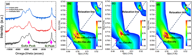
Figure 3. (a) X-ray diffraction omega-2theta (004) rocking curves for three different DFLs structures, where the peaks of GaAs and Si are labelled in the diagram; reciprocal space maps measured around the asymmetric reflection (224) for (b) InAlGaAs ASG, (c) InGaAs/GaAs SLSs and (d) InGaAs ASG, where Q(x) is parallel to the in-plane [110] direction and the Q(z) axis is parallel to the GaAs growth [001] direction, and the scale bars show the log intensity range of the maps.
Download figure:
Standard image High-resolution imagewhere  and
and  are the lattice constant of in-plane and growth direction respectively, which can be extracted from the plot of RSM results.
  is the corresponding bulk lattice constant of epitaxial material and
  is the Poisson ratio of GaAs which is equal to 0.31. Derived from the RSM data, the InAlGaAs ASG presents a 95% relaxation in In0.05Al0.35Ga0.6As layer and 89% relaxation in In0.1Al0.7Ga0.2As layer with respect to GaAs, while the InGaAs ASG provides a 97% relaxation in In0.05Ga0.95As layer and 88% relaxation in In0.1Ga0.9As layer with respect to GaAs. However, the InGaAs in SLSs structure has only 32% relaxation with respect to GaAs. The RSM results show that the low indium composition ASG structures have a similarly higher level of strain relaxation than the SLSs, which is believed to be conducive to reducing TDD [16].
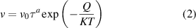
Raman spectroscopy has also been used to reveal the crystal quality. Raman spectra were taken under the backscattering geometry; the excited photons will penetrate about 140 nm into GaAs and only bring spectra data of the GaAs film. As presented in figure 4(a), the strong peak that appearing at 289 cm−1 is referred to be the frequency of the GaAs longitudinal optical (LO) phonon while another weak peak occurs at the phonon frequency of 265 cm−1. The inset in figure 4(a) is the transverse phonon (TO). The LO peaks are normalised to a maximum value of 1 to facilitate comparisons across the TO peaks of different DFLs. The growth direction of the GaAs layer is in the [001] direction and the received spectra from the backscattering geometry are from the (100) surface plane. The polarisation of a TO phonon is vertical to the [100] direction with the Raman tensor of R(y) and R(z) should not appear in (100) surface in backscattering mode. Therefore, the TO peak in this case is only considered as an indication of the crystal imperfections, such as the TDs [25–27]. The value of the TO peak is 0.08, 0.2 and 0.276 of the samples with InAlGaAs ASG, InGaAs SLSs, and InGaAs ASG, respectively. The full width at half maximum (FWHM) of the LO peak and the normalised TO peak intensity for these three samples are compared in figure 4(b). It is clear that the sample with InAlGaAs ASG structure has the highest ratio of the peak intensity of the LO peak to that of the TO peak, indicating that it has the best GaAs crystal quality among these three samples.
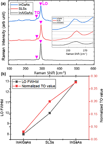
Figure 4. (a) Normalised Raman spectroscopy for different DFLs structures, (b) the comparison of the FWHM of the LO peak and the normalised TO peak intensity extracted from figure 4(a). The inset of figure 4(a) is the megascope of the TO peak in the Raman spectra.
Download figure:
Standard image High-resolution imageComparing these two highly relaxed ASG structures, since the covalent single-bond radii of aluminium (126 pm) and gallium (124 pm) are nearly identical, as well as the lattice constant of InGaAs and InAlGaAs, the applied stress from them to TDs should be nearly identical [28]. The introduction of aluminium substituting part of the composition from gallium will not inhibit the movement of gliding TDs during the deformation process [29]. Nevertheless, considering this quaternary material as a dilute alloy system, the other mechanical properties of AlAs, such as bulk modulus, shear modulus and Poisson's ratio are greater than those of GaAs, and thus bring a hardening effect to this quaternary alloy. Here, aluminium could act as a hardening agent to the original InGaAs structure to increase the hardness characteristics of the whole layer [29–31]. The velocity of any type of dislocations  inside various semiconductor structures is proportional to the stress
  , which is empirically identified as
where  a are the constants,
  is the applied stress [32]. The applied stress
  is an athermal stress which is the sum of the shear stress added to the TD segment on its gliding plane and the line tension of the MD, which can be derived as
where  and
and  are the shear modulus and the Poisson's ratio of the epitaxial layer respectively;
  is the thermal biaxial strain; A, B and C are the constants of the trigonometric values of the angle between the glide plane and the interface and the Burger vector's angle; R is a finite interaction radius and d is the distance from MD to the interface. As the shear modulus and the Poisson's ratio of AlAs are greater than those of GaAs, we can obtain a higher dislocation velocity with the accession of aluminium to the original InGaAs ASG structure [33]. In one of the principal TDD reduction strategies, the encounters between TDs lead to the dwindling of TDD under the interaction area. The higher velocity of glissile TDs leads to a higher possibility of the self-annihilation of TDs, for those with the opposite Burger vector will be self-annihilated when they meet. Therefore, with the similar strain relaxation level inside of the InGaAs ASG and InAlGaAs ASG structures, the InAlGaAs quaternary alloy can offer a higher applied stress
  to the TDs and promote the procedure of the self-annihilation of TDs.
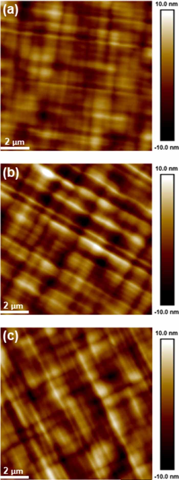
Although ECCI images have already revealed the surface, the surface smoothness condition and contrast can be obscured by the backscattering mode. AFM measurements were also carried out to investigate the surface morphology of the GaAs buffer layers. About 10 μm × 10 μm AFM images were taken and are shown in figure 5 to compare the surface morphology of the top GaAs layer upon these three different buffers. It can be seen that the crosshatch pattern is less prominent in the InAlGaAs ASG structure, revealing the exquisite quality of the underlying layer and also showing the lowest root-mean-square (rms) roughness of only 2.07 nm, which is 37.2% and 29.4% lower than the InGaAs/GaAs SLSs and InGaAs ASG structure respectively. The rms values are derived from the 10 μm × 10 μm AFM images.

Figure 5. About 10 × 10 μm2 AFM images of the surface of as-grown top GaAs layer upon (a) InAlGaAs ASG structure with rms of 2.07 nm; (b) InGaAs/GaAs SLSs with rms of 2.84 nm; (c) InGaAs ASG with rms of 2.68 nm.
Download figure:
Standard image High-resolution imageTo further compare and analyse the TD annihilation mechanism in the different DFL, cross-sectional TEM measurements are used. All the DFL structures showed a misfit dislocation array in both the top and the bottom regions (figure 6). In all three systems InAlGaAs ASG structure (figure 6(a)), InGaAs/GaAs SLSs (figure 6(b)) and InGaAs ASG (figure 6(c)) TD annihilation occurs through their lateral movement, demonstrated by the misfit dislocations generated in DFL area [19].
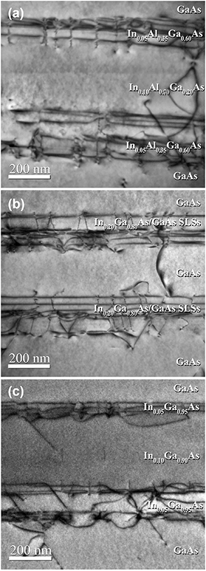
Figure 6. Bright-field cross-sectional TEM images showing the TD annihilation in different types of DFLs: (a) InAlGaAs ASG structure; (b) InGaAs/GaAs SLSs; (c) InGaAs ASG.
Download figure:
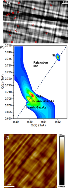
Standard image High-resolution imageThe HRXRD, Raman spectroscopy along and AFM results provide strong evidence that the InAlGaAs is effective in reducing TDs and provides the best quality of GaAs layer. After reviewing the TD reduction mechanism and the high performance of the InAlGaAs ASG buffer, we decided to further optimise this structure and reduce the total buffer thickness to less than 2 μm by decreasing the thickness of the GaAs layer from 1350 nm to 1050 nm. Due to the difference in thermal expansion coefficient difference between III–V material and Si, once the total thickness of III–V material exceeds 7 μm, it will cause thermal cracks in several millimetre in length and reduce the yield of III–V/Si devices [9]. Considering the kinetic constraints are another significant factor in this system, additional thermal annealing at 500 °C for 10 min is applied to each InAlGaAs layer inside the DFL under the arsenic overpressure to alleviate the strain released with thinner underlying GaAs layer. After reducing the buffer thickness by 15%, the average surface TDD is substantially reduced to 6.3 × 106cm−2 with a standard deviation of 0.102, which indicates that the average TDD is even lower than that of the 2.3 μm InAlGaAs buffer. A representative ECCI of the layer is shown in figure 7(a), while figure 7(b) shows the RSM measured around the asymmetric reflection (224) for this sample. It can be deduced from the results in figure 7(b) that the relaxation for In0.05Al0.35Ga0.6As and In0.1Al0.7Ga0.2As are calculated to be 80% and 45% correspondingly. Figure 7(c) spotlights the uppermost surface morphology of this thickness reduced InAlGaAs ASG with a rms roughness of 2.66 nm. The smooth uppermost surface reflects this epitaxial layer with low defect density and irregularities. An appropriate thermal annealing condition not only promotes a relatively high level of strain relaxation in the In0.05Al0.35Ga0.6As and In0.1 Al0.7Ga0.2As but also provides the activation energy for glissile TDs, which leads to a high efficiency in TD reduction. This shows that the athermal stress from the mechanical properties of the buffer material can have a synergistic effect with the thermal stress to stimulate the self-annihilation of TDs.
Figure 7. (a) Representative ECCI scanning image of the 2 μm InAlGaAs ASG structure. (b) Reciprocal space maps measured around the asymmetric reflection (224) for 2 μm InAlGaAs ASG. (c) About 10 × 10 μm2 atomic force microscopy images of the surface of the as-grown top GaAs layer upon the 2 μm InAlGaAs ASG structure with rms of 2.66 nm.
Download figure:
Standard image High-resolution image
4. Conclusion
The potential of monolithic integration of compound semiconductors on silicon is commanding recognition due to its potential for comprehensive photonic integration, while still facing the drawback of the thick buffer layer and the flawed crystal quality. Here we proposed and examined a new DFL, InAlGaAs ASG, and obtained the lowest average TDD value, compared to other DFL structures, such as the InGaAs ASG and InGaAs/GaAs SLSs. The TDD was reduced to 6.3 × 106 cm−2 within a 2 μm III–V buffer grown on Si. The mechanism of how this quaternary alloy works to reduce TDD has been proposed. It was observed that aluminium acts as an effective hardening agent in the DFL structure to increase the velocity of glissile TDs, thus further promoting the self-annihilation of TDs. In addition, the coordination of this thin buffer layer with a manageable lower cooling rate after the growth offers an improved solution for the thermal cracks. This InAlGaAs ASG buffer is believed to have promising potential, especially for InAs/GaAs quantum dot laser devices as well as being suitable for various III–V on Si integration applications to enable better device performance.
Acknowledgments
This work was supported by the UK Engineering and Physical Sciences Research Council (EP/P006973/1, EP/R029075/1, EP/T028475/1 and EP/X015300/1).
Data availability statement
All data that support the findings of this study are included within the article (and any supplementary files).