
Abstract
Erosion of an aluminium oxide surface as well as a formation of an aluminium oxide coating on an aluminium substrate, comparable with erosion and oxide formation induced by plasma electrolytic oxidation (PEO), can be caused at atmospheric pressure conditions by a DBD-like (dielectric barrier discharge) plasma jet. Obtained experimental results conform a previously assumed similarity of the erosion mechanisms induced by the atmospheric pressure DBD-like plasma jet and PEO microdischarges. The mechanism of a predominantly inward growth of the oxide layer during PEO processing is substantiated based on a comparison of aluminium oxide erosion and oxide layer deposition by a treatment with the considered He-plasma jet and a PEO process.
Export citation and abstract BibTeX RIS

Original content from this work may be used under the terms of the Creative Commons Attribution 4.0 license. Any further distribution of this work must maintain attribution to the author(s) and the title of the work, journal citation and DOI.
1. Introduction
Surface processing is a major field in plasma technology. Various systems, ranging from low pressure over atmospheric pressure systems as well as plasma inside or in contact with liquids, are applied to achieve unique surface properties. One example in surface processing of light metals is plasma electrolytic oxidation (PEO). PEO allows the creation of durable, thick, uniform coatings with high corrosion resistance on light metallic components. The formed coatings are strongly adhered to the treated objects. Despite the huge number of published studies (see for instance reviews [1–4]) and the expected broad field of applications, a fundamental understanding of the basic mechanisms of the PEO process remains far from complete. This process includes a formation of a large number of short-living microdischarges, which appear stochastically on the treated surface. These transient microdischarges cause an extraction of substrate material, an enhancement of atomic oxygen evolution, a heating of the top layer of the treated surface as well as the formation of a crystalline oxide layer [5–8]. A characterisation of the plasma conditions of these microdischarges can be helpful for an understanding of the fundamental physical process during PEO and an knowledge-based process optimisation customised to its various applications. In previous studies, individual microdischarges were studied on an anode with a reduced active surface with diameter of 1 mm [9–11]. Nevertheless, from a plasma scientific point of view, the microdischarges during PEO are highly challenging due to their transient nature, the interplay of all aggregate phases, the limited optical access, etc. Therefore, a transfer to other microdischarges under more controllable plasma conditions, but with comparable properties like PEO microdischarges, possibly can also support a further development of a plasma physical model of the PEO processes.
On the other hand, non-equilibrium atmospheric pressure plasma jets were extensively studied as tools for various surface processing technologies of different materials [12, 13]. Plasma jets operated at atmospheric pressure conditions can induce erosion on metallic and other substrates or, in contrast, can be used for the deposition of coatings on various substrates. Therefore, a comparison between the surface modifications induced by a He-plasma jet and PEO microdischarges possibly can support a better understanding of the plasma-solid interactions as well as microdischarge characteristics during PEO.
In a previous study [14], an amorphous aluminium oxide film was deposited on an aluminium substrate by a high voltage anodisation process and afterwards treated with microdischarges during high voltage PEO and with microdischarges at atmospheric pressure, namely a self-organized DBD (dielectric barrier discharge) and a DBD-like plasma jet operated with He/N2 (95%/5%) gas flow. Despite strong differences in measured discharge characteristics the observed erosion trace characteristics, especially dimension, form and material distribution, left by all three microdischarges on the aluminium oxide surface were very similar and hence, a similar formation mechanism was assumed. Based on results of previous studies [14–19], the formation of plasma spots with a core and with a helical electric current and toroidal heating of the treated surface, was supposed. The following general conclusions of those studies were drawn: (a) a relatively cold plasma with a diameter of several hundred micrometers can be contracted to a plasma spot core with a diameter of about one micrometre, (b) the treated material can be destructed and partially extracted without melting and vaporisation, (c) plasmoids can be produced in the afterglow phase of plasma spots [19]. Plasmoids describe narrow plasma objects without visible connection to a powered electrode. These effects cannot be explained in the frame of a known conventional theoretical model and only a hypothesis presented in [20] and discussed in [21] can be used to qualitatively interpret this effect. Despite the fact that no theoretical model can be currently used to sufficiently explain the considered event and additional theoretical and experimental studies are needed, this effect, can be possibly used in different applications e.g. for the gas flow conversion at high gas temperatures (5000 K–6000 K) in a plasma plume of gliding arc channels without overheating of the electrodes [18]. Further co-studying of microdischarges under atmospheric pressure conditions and during plasma electrolysis is a new approach to conform or disprove the assumption of physical model equality and expand knowledge on both plasmas.
In the presented study, well-known experimental techniques are applied to on the one hand, evaluate possibilities to induce a PEO-like surface oxidation by another atmospheric plasma source and hence, partially clarifying the role of PEO microdischarges on the coating growth during PEO. On the other hand, no defined proven physical model of PEO microdischarges exists so far. To figure out their ignition process and microdischarge nature, it is helpful to understand, how microdischarges can penetrate through slits and defects in dielectric coatings and if PEO microdischarges interact in a comparable way with certain surfaces like other atmospheric pressure plasma sources. Therefore, aluminium substrates and aluminium substrates pretreated with an anodisation procedure are treated with a DBD-like He-plasma jet and PEO process based on the first results presented in [14]. At that, gas flow swirls, a formation of artificial hot spots using substrate surface scratching, and an anodising pretreatment are used for the instigation of material erosion and possibly oxidation by the considered He-plasma jet. In this work, erosion describes a plasma-induced removal or destruction of surface material of the treated substrates. An additionally applied thin gold layer on the treated surface enables the visualisation of the traces of active microdischarges and their afterglow during PEO and the plasma jet treatment. The temporal behaviour of the PEO microdischarges on the surface of the amorphous aluminium oxide film is studied by the usage of a high-speed charge-coupled device (CCD) camera. Dimension, form, structure and material composition of plasma induced defects on the treated surfaces are characterised by scanning electron microscopy.
2. Experimental set-up
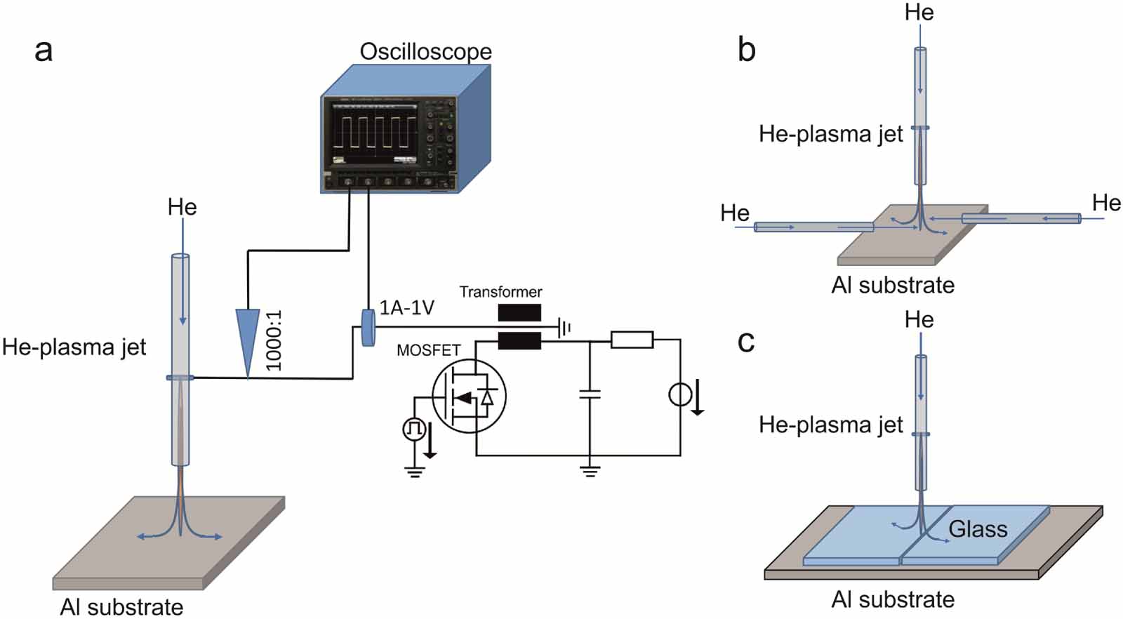
A schematic experimental setup for the considered DBD-like He-plasma jet is shown in figure 1(a). Pure helium (Alphagaz, 5.0) is transported with a gas flow of 500 sccm through a quartz capillary with an inner diameter of 1 mm and a wall thickness of 0.25 mm. A high-voltage electrode (a coiled copper wire) is placed around the quartz tube at a distance of 20 mm from the open end of the capillary. The high-voltage pulse sequences have a repetition frequency of 4 kHz and a sequence duration of 10 μs. Each sequence consists of high-voltage pulses (up to about 20 kV) with a frequency of about 700 kHz and a damped amplitude. The applied voltage and electric current are measured using an oscilloscope (Waverunner 204 Xi-A, 2 GHz, Teledyne LeCroy) with a capacitive voltage divider (P6015A, Tektronix) and current probe (Model 2877, Pearson Electronics), respectively. As substrate, small plates of an aluminium alloy (AW-6061) with a dimension of 20 mm × 20 mm × 2 mm are used. The gas flow dynamics of the plasma jet effluent can be influenced by additional lateral gas flows. Figure 1(b) displays a schematic sketch of the experimental setup with an additional gas flow realised by a helium flow through similar capillaries as the quartz capillary of the plasma jet. Two additional gas flows, which amount to 1 slm, produce gas flow swirls on the substrate surface (see figure 1(b)).

Figure 1. Schematic view of the experimental setup used to study the interaction of the effluent of a DBD-like He-plasma jet with an aluminium substrate or aluminium substrate covered with an aluminium oxide layer (a). Figures (b) and (c) present experimental setups used to study the interactions of the plasma jet with a gas flow swirl (b) and a dielectric slit (c) created by two glass plates directly on the aluminium sample for the instigation of aluminium (or aluminium oxide) substrate erosion.
Download figure:
Standard image High-resolution imageTo study an influence of a thin dielectric slit on the erosion of aluminium or an aluminium oxide layer during the treatment with the He-plasma jet, the substrate surface is covered with two glass plates of 1 mm thickness and with polished edges (Thermo Fisher Scientific Menzel-Glaeser). These plates are pressed together (see figure 1(c)). The slit width is measured using an electron microscope and amounts to about 20 μm. During the substrate treatment, the plasma jet nozzle is moved with a velocity of about 1 mm s−1 along the slit. The distance between the plasma jet nozzle and the glass plates surface amounts to 2 cm.
The schematic experimental setup for the PEO process is presented in figure 2. A cylindrical, double-walled borosilicate vessel is used as electrolytic cell. Two opposite, optical-grade, quartz glass windows with a diameter of 40 mm ensure light transmission down to λ = 200 nm. A stainless steel cylinder with a diameter of 4 mm is used as cathode. The substrates for the PEO process are aluminium AW-6061 plates with a dimension of 20 mm × 20 mm × 2 mm, as well. These substrates serve as anode during the process. During the first anodisation phase of the PEO process, a thin porous and rough oxide film with a thickness of about a micrometre is deposited. This first anodisation phase is imitated by a high voltage anodisation treatment of 3 min at a direct current (DC) voltage of 250 V and current density related to the anode surface of approximately 0.125 Acm−2. To ensure, that no breakdown appears, the voltage 250 V is chosen, which is roughly in the middle between the typical maximum of anodisation voltages at around 80 V and the breakdown voltage of the PEO process at around 470–480 V in this setup. Distilled water with the addition of 1 g l−1 potassium hydroxide serves as electrolyte for both processes, the preliminary anodisation and the PEO process. After the pre-processing the substrates are rinsed with distilled water and some of the pretreated substrates are covered with a 5 mm × 5 mm square gold layer in a JEOL JFC-1200 fine coater. These coated and the other non-coated substrates are treated in a PEO process and with the plasma jet. The PEO process is also performed with a current density related to the anode surface of approximately 0.125 Acm−2. The substrates without a gold layer are treated for 1 min at a voltage of 750 V. The substrate with gold layer are treated with a DC pulse of 40 μs and 750 V, due to an extensive plasma ignition on the gold layer.

Figure 2. Schematic sketch of the experimental setup used for the preliminary anodisation and the plasma electrolytic oxidation treatment of aluminium substrates at direct current (DC) voltage.
Download figure:
Standard image High-resolution imageThe temporal behaviour of the PEO microdischarges on the surface of the amorphous aluminium oxide film is studied using a high-speed camera (Phantom VEO 440L 1MP; Vision Research). The camera settings, camera frame rate of 10 000 fps, exposure time of 99 μs and image resolution of 512 × 512 pixels, are matched for a reliable study of the temporal behaviour of the microdischarges. The structure and composition of the treated substrates are characterised by surface scanning electron microscopy and energy dispersive x-ray spectroscopy using a scanning electron microscope (SEM)/energy dispersive x-ray spectroscopy (EDS) microscope (JSM6510, JEOL).
3. Experimental results
3.1. Interactions of the He-plasma jet with untreated aluminium substrates
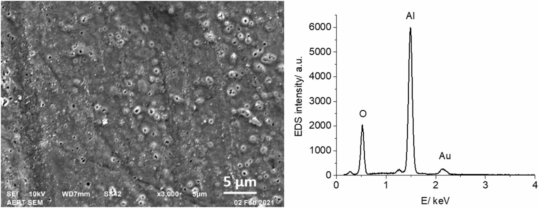
A SEM image of a polished untreated aluminium substrate is presented in figure 3. Figure 4 shows SEM images and EDS spectra of an analogous prepared aluminium substrate after a 5 min treatment with the He-plasma jet. Current–voltage characteristics of the treatment are very similar to those presented in [14] and are not presented here. During the treatment the distance between the nozzle of the plasma jet and the substrate surface amounts to 2 cm. No erosion traces are observed in the treated area with a radius of approximately 400 μm around the He-plasma jet axis. Near the border of this area, a thin oxide layer is deposited. The zoomed SEM image in figure 4 shows the structure of the surface and an EDS spectrum presents the material composition in this border area. The measured relative material composition in this area amounts to O: Al = 0.3.

Figure 3. SEM image of the surface of an aluminium substrate after preparation, namely polishing and washing.
Download figure:
Standard image High-resolution image
Figure 4. SEM image of an aluminium substrate after a treatment with the He-plasma jet. The treatment time amounts to 5 min. The zoomed image and EDS spectrum present the surface structure and material composition at the edge of the treated area, respectively.
Download figure:
Standard image High-resolution imageAs variation, the effect of an additional He gas flow swirl on the plasma surface interaction is studied (figure 1(b)). A corresponding SEM image and an EDS spectrum measured on the aluminium substrate treated for 5 min with the He-plasma jet combined with an additional He gas flow swirl are presented in figure 5. Again, the treated area is approximately circular with a radius of 400 µm. Despite the absent of erosion traces in the middle of this treated area, at the edge of this area erosion traces and holes with the formation of aluminium oxide are observed. The measured relative material composition in this edge area amounts to O: Al = 1.4, which corresponds to a material composition close to aluminium oxide ceramic. The produced oxide appears as a layer with a very inhomogeneous structure and material composition (see zoomed SEM image and EDS spectra in figure 5).

Figure 5. SEM image (on the top) of an aluminium substrate after a treatment with the He-plasma jet combined with a He gas flow swirl like introduced in figure 1(b). The treatment duration amounts to 5 min. The zoomed image and EDS spectra on the top present the surface structure and material composition of the oxide layer produced in the border region of the treated area, respectively. Erosion traces and holes get visible.
Download figure:
Standard image High-resolution imageBased on results presented in [17] concerning the importance of a 'hot-spot' formation for plasma surface interactions and the enhancement of Ti layer erosion, a scratch on the aluminium surface is used in this work, which is artificially produced with a diamond blade. After scratching, the aluminium substrate is treated in the effluent of the He-plasma jet. During this treatment, the jet is moved along the scratch with a velocity of about 1 mms−1. In several places erosion traces are located (see figure 6) near the scratch. An exemplary erosion area is presented in the zoomed SEM image in figure 6. Some structures with a material composition of O: Al = 1.3 can be detected, which can give a hint on oxide species. Also aluminium areas are observed in EDS spectra, illustrated in figure 6, as well. The comparably small peak at 2.12 keV in the EDS spectra is caused by a thin (approximately 13 nm) gold layer, which is deposited to exclude overcharging of the substrate surface during electron microscopy.

Figure 6. SEM images of an aluminium substrate after a treatment with the He-plasma jet near a scratch previously produced by a diamond blade (on the bottom). The He-plasma jet was shifted with a velocity of about 1 mms−1 along the scratch. The zoomed image and EDS spectra on the top present the surface structure and material composition of an exemplary erosion area, respectively. A thin gold layer with a thickness of approximately 13 nm is deposited to exclude overcharging of the substrate surface during electron microscopy.
Download figure:
Standard image High-resolution image3.2. Interactions of the He-plasma jet with substrates through a dielectric slit
Based on results presented in [22, 23], where microdischarges penetrate holes and thin slits in a dielectric and cause hydrocarbon erosion and crystals deposition, this effect is studied as a third option to enhance the erosion on an aluminium substrate. In those studies, the occurrence of plasmoids and their interplay with the substrate surfaces are mentioned to cause the erosion of hydrocarbon films with a high efficiency. To verify this assumption, a slit between two glass plates with polished edges is created (see figure 1(c)). These plates are directly placed on the aluminium substrate. The distance between the plate edges is measured with the electron microscope and amounts to approximately 20 μm. It is assumed, that the gap between the aluminium substrate and glass plates is in the same range. The He-plasma jet is used for a treatment of the top surface of the plates and is moved along the slit with a velocity about 1 mms−1. After that, the dielectric glass plates are removed and the aluminium substrate is covered with a thin gold layer (about 13 nm) to exclude overcharging of the substrate surface during electron microscopy. The SEM image in figure 7 shows an exemplary segment of the aluminium substrate underneath the treatment area. The position of the slit edges is presented with dashed lines. The zoomed SEM image and the respective EDS spectra show the structure and the material composition of the treated aluminium surface in the slit area. The aluminium surface is modified not only in the slit region, but also in the area between the glass plates and aluminium substrate. In the presented SEM image (figure 7) areas with erosion traces are observed at a distance up to 85 μm from the slit centre. Consequently, microdischarges penetrate not only through the thin slit between the glass plates, but also spread in the slit between the glass plates and the aluminium substrate. The zoomed SEM image and EDS spectra in figure 7 present the surface structure and material composition (O: Al = 1.4) of a deposited aluminium oxide layer. Based on the velocity of the He-plasma jet movement along the dielectric slit and the width of the plasma spot on the dielectric surface a deposition rate can be roughly estimated. It is supposed to reach a high value of up to 10 μms−1. After treating the glass plate with the plasma jet at a sufficiently large distance from the slit (10 mm), no erosion traces are observed on the aluminium substrate underneath the glass. Therefore, partial discharges in the gap between the dielectric glass and metal as a possible reason for the observed erosion and deposition of the oxide layer can be excluded from consideration [23].

Figure 7. SEM images of the aluminium substrate after a treatment with the He-plasma jet through the narrow slit between the polished edges of the glass plates (on the bottom). The width of the slit amounts to about 20 μm. Dashed lines show the approximate position of the glass plate's edges. The He-plasma jet was shifted during the treatment with a velocity of about 1 mms−1 along the slit (figure 1(c)). The zoomed image and EDS spectra on the top of the figure present the surface structure and material composition of erosion traces and holes, respectively. A thin gold layer with a thickness of approximately 13 nm is deposited to exclude overcharging of the substrate surface during electron microscopy.
Download figure:
Standard image High-resolution image3.3. Interactions of the He-plasma jet with anodised aluminium substrates
To compare the erosion mechanism of microdischarges at atmospheric pressure and during a PEO process, the interaction of the He-plasma jet with an aluminium oxide layer produced by anodising is studied. A SEM image of an exemplary aluminium substrate surface after 3 min anodising at a voltage of 250 V and a maximum current of 1 A is presented in figure 8. In comparison to the aluminium substrate shown in figure 3, the amorphous aluminium oxide film, grown on the aluminium substrate surface, gets visible (see figure 8). The measured ratio of the oxygen and aluminium density determined from EDS spectra amounts to O: Al = 0.9 and hence, differs from an expected value of 1.5 for aluminium oxide. A possible reason for this difference is the low thickness of the deposited oxide layer and the penetration depth of high energetic electrons of the electron microscope during EDS. The EDS detector of the used electron microscope collects information of the material composition from a depth of more than 1 μm. In the presented study, EDS delivers only qualitative information concerning material composition of substrate surface, since the resolution of the measurements is in the same range like the dimensions of the oxide layer of about 1 μm thickness and erosion structures at about 1 μm scale. Therefore, the measured EDS spectra and relative aluminium and oxygen intensities instead of numerical data concerning the material composition are presented in this study.

Figure 8. SEM image of an aluminium substrate surface after 3 min anodising at a voltage of 250 V and a current density of 0.125 Acm−2 (left). An EDS spectrum of the top layer of the substrate surface is shown as well (right). A thin gold layer with a thickness of approximately 13 nm is deposited to exclude overcharging of the substrate surface during electron microscopy.
Download figure:
Standard image High-resolution imageThe amorphous oxide film shown in figure 8 is strongly modified by a treatment with the He-plasma jet (see figure 9). Erosion traces appear as groups with different expansions on the treated surface (see figure 9(a)). Both, erosion craters and channels, can be observed on the treated surface. A form of craters produced with this treatment appears as eruption crater (see figure 9(c)) with a diameter of approximately 2 μm. The measured relative material composition at the borders of these erosion craters and channels amounts to about O: Al = 1.5. A characterisation of the material composition using the EDS spectrum in the hole shown in figure 9(c) is only possible, since the detection angle of the used SEM/EDS is small enough. Hence, the diameter of the hole combined with its comparable low depth is sufficient for a reliable EDS signal intensity.

Figure 9. SEM images of an anodised (250 V, 0.125 Acm−2, 3 min) aluminium substrate after a treatment with the He-plasma jet (a). The treatment duration amounts to 5 min. Zoomed SEM images and EDS spectra measured on surface of the treated substrate area (b). The zoomed image and the EDS spectra of an erosion crater (c) show the surface structure and material composition, respectively. A thin gold layer with a thickness of approximately 13 nm is deposited to exclude overcharging of the substrate surface during electron microscopy.
Download figure:
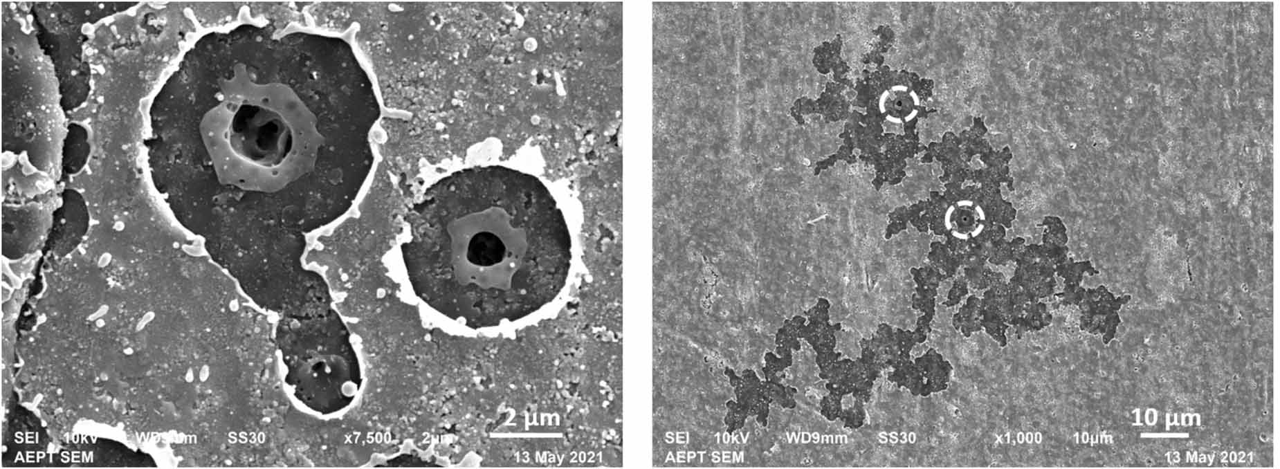
Standard image High-resolution imageTo better visualize the plasma interaction with the treated surface an additional gold layer is deposited before a plasma treatment based on results presented in [14, 16]. Similar to [16], a gold layer with a thickness of 100 nm on the surface of a pretreated aluminium substrate stops the erosion process completely. A relative thin gold layer (50 nm) influences erosion processes less, but also gives the possibility to observe the activity of microdischarges on the substrate surface with a high contrast [14]. A pre-anodised aluminium substrate (250 V, 0.125 Acm−2, 3 min) covered with a 50 nm gold layer was treated with the He-plasma jet. The surface of the treated sample is studied with the electron microscope (see figure 10). In areas with a high number density of erosion traces the SEM images of the treated substrate surfaces with and without a thin gold layer are very similar, as can be seen in a comparison to figure 9. Because of the partial overlapping of different erosion traces, the interpretation of these images is very complicated. At the border of these areas, some separated erosion traces can be observed (see figure 10). These traces on the gold layer show a spatial distribution of temperature in a plasma spot of microdischarges and moving traces of microdischarges on the substrate surface during their lifetime and in an afterglow phase. Diameter of erosion traces at start and end points are different and can support an interpretation of the microdischarge activity on the treated surface. An interesting example of such microdischarge activity is shown in figure 10 (left), where the SEM image shows two microdischarge traces, with and without afterglow phase. The SEM image on right hand side of figure 10 shows large erosion areas mainly induced by plasmoids, which are formed in the afterglow of two microdischarges, which positions are marked with dashed circles.

Figure 10. SEM images with different magnification of an anodised aluminium substrate (250 V, 0.125 Acm−2, 3 min) after a treatment with the He-plasma jet. Before the treatment, the substrate was covered with a gold layer of 50 nm thickness. The SEM image on left hand side shows two deep erosion traces with and without a formation of an afterglow phase (plasmoid). An erosion activity of plasmoids on the treated surface can form separated eroded areas, which are presented on the right hand side. Deep erosion traces of microdischarges are marked with dashed circles in the right image.
Download figure:
Standard image High-resolution imageAs before, to check the influence of a dielectric slit on the efficiency of erosion processes the experimental set-up presented in figure 1(c) is used. It is the same arrangement used for the previously shown enhancement of the erosion of uncoated aluminium (see figure 7). Now, the aluminium substrate was anodised at 250 V and a maximum current of 1 A (current density of 0.125 Acm−2) for 3 min and is treated with a He-plasma jet through the dielectric slit between two polished glass plates as presented in figure 1(c). During this experiment, the plasma jet is moved along the dielectric slit with a velocity of about 1 mms−1. Similar to the treatment of uncoated aluminium, erosion traces and holes are distributed not only in the area of the slit, which width amounts to about 20 μm, but also under the glass plate up to 85 μm from the central axis of the slit (see figure 11). The measured relative material composition at the borders of erosion craters and channels amounts to about O: Al = 1.5. At the same time, mainly aluminium is found in the centre of broad eroded channels (see EDS spectrum on the left side of figure 11) and a low oxygen content is determined with EDS spectra measured inside of small eroded holes (O: Al ∼ 1.1). As before, no erosion traces can be observed on the substrate under the glass plate after a plasma treatment of the glass surface at a distance of approximately 10 mm from the slit.

Figure 11. SEM image of an anodised aluminium substrate (250 V, 0.125 Acm−2, 3 min) after a treatment with the He-plasma jet through a narrow slit between polished edges of glass plates (on the bottom). The width of the slit is about 20 μm. Dashed lines show the approximate position of the glass plate's edges. The He-plasma jet was shifted during the treatment with a velocity of about 1 mms−1 along the slit (figure 1(c)). The zoomed image and EDS spectra on the top present the surface structure and material composition of erosion traces and holes, respectively. A thin gold layer with a thickness of approximately 13 nm is deposited to exclude overcharging of the substrate surface during electron microscopy.
Download figure:
Standard image High-resolution image3.4. The effect of a short PEO process on anodised aluminium substrates
As comparison, an anodised aluminium substrate (250 V, 0.125 Acm−2, 3 min) is treated with a short PEO process (750 V, 0.125 Acm−2, duration 1 min). The high-speed camera image in figure 12 shows the PEO microdischarges, which are mainly distributed near the substrate edges of the treated substrate during this short process. Corresponding SEM images and EDS spectra reveal the surface structure and material composition of the substrate top layer as shown in figure 13. The structure of this surface shows similarities to the structure of a substrate surface treated with the He-plasma jet presented in figures 10 and 11. Both, erosion craters and long erosion traces with comparable dimensions, can be observed in these images. The long microdischarge erosion traces are characterised by a thin molten and solidified layer, which can be observed in both SEM images in figure 13. EDS spectra presented in figure 13 show, that the amount of oxygen increases in these long erosion traces compared to nearby not molten areas with a ratio of oxygen to aluminium of O: Al = 1.1–1.3. The ratio of oxygen to aluminium at microdischarge crater cones and inside of craters amounts to 1.5 and 0.8, respectively.

Figure 12. High-speed camera image of an anodised aluminium substrate (250 V, 0.125 Acm−2, 3 min) during a short PEO treatment (750 V, 0.125 Acm−2, 1 min). The exposure time of the camera amounts to 0.1 ms.
Download figure:
Standard image High-resolution image
Figure 13. SEM image and EDS spectra of an anodised aluminium substrate (250 V, 0.125 Acm−2, 3 min) after a short PEO process treatment (750 V, 0.125 Acm−2, 1 min) (left). The zoomed image (right) and the corresponding EDS spectra show the surface structure and material composition of erosion traces, respectively. A thin gold layer with a thickness of approximately 13 nm is deposited to exclude overcharging of the substrate surface during electron microscopy.
Download figure:
Standard image High-resolution imageAnalogous to the previous He-plasma jet treatment, a thin gold layer on an anodised surface is used to observe the microdischarge activity during a PEO process. Therefore, the anodised aluminium substrate (250 V, 0.125 Acm−2, 3 min) is covered with a thin gold layer (5 mm × 5 mm × 50 nm) in the middle of a substrate by using a silicone mask and afterwards treated with a short PEO process (750 V, 0.125 Acm−2, 40 μs). The gold layer causes a decrease of the ignition voltage of microdischarges below 200 V. Because of the short duration time of this treatment and the small dimension of the gold layer, it is possible to observe the ignition of all single microdischarges. This enables a correlation of single microdischarges and erosion traces left by these microdischarges on the substrate surface using a high-speed camera and electron microscopy (see figure 14). Microdischarges of varying intensity and varying form and size are observed with a high-speed camera. Corresponding SEM images reveal both, deep microdischarge craters and long shallow erosion traces, shown in the second row of figure 14.

Figure 14. High-speed camera image of an anodised aluminium substrate (250 V, 0.125 Acm−2, 3 min) after a short PEO process treatment (750 V, 0.125 Acm−2, 40 µs) (on the top). Before the treatment, a part of the substrate (dark grey square) was covered with a gold layer of 50 nm thickness. The exposure time of the high-speed camera amounts to 0.1 ms. The zoomed image shows a part of the gold-covered surface and the corresponding SEM image is presented on the bottom. The dashed ellipse and rectangle in the SEM image show the areas of the microdischarges (areas of intensive emission) observed in the camera image on the top. The zoomed image (dashed rectangle) on the bottom presents the surface structure of erosion traces.
Download figure:
Standard image High-resolution image3.5. Interactions of PEO microdischarges and the He-plasma jet on thick PEO coatings
To study a deep and shallow erosion caused by PEO microdischarges on a thick oxide film, an aluminium substrate was prepared with a long PEO process (750 V, 0.125 Acm−2) of 30 min duration and covered with a thin gold layer (50 nm), as before. Afterwards, this substrate was treated with a short PEO process (750 V, 0.125 Acm−2, 40 µs). Similar microdischarges as on a thin oxide film can be observed during this short treatment by using the high-speed camera. But in contrary, no deep erosion traces are established on the gold coated substrate surface. Shallow erosion traces in the gold layer can be found mainly near the cracks of the former oxide layer (see figure 15). Some of these microdischarges seem to induce long shallow erosion traces with a broadness of approximately 2 μm. No remarkable damages of the underlying oxide layer can be observed in the traces of these microdischarges near cracks and in the long shallow erosion traces.
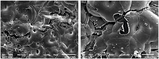
Figure 15. SEM image of pretreated aluminium substrate (PEO, 750 V, 0.125 Acm−2, 30 min) in the area of the additional square gold layer (5 mm × 5 mm × 50 nm) after an additional short PEO treatment (750 V, 0.125 Acm−2, 40 µs). Shallow erosion traces can be observed near cracks in the previous PEO oxide coating.
Download figure:
Standard image High-resolution imageA similarly prepared aluminium substrate (750 V, 0.125 Acm−2, 30 min) with an additional gold layer is treated with the He-plasma jet. Corresponding SEM images of the treated surface show both, deep craters and shallow erosion channels (see figure 16). The deep erosion craters can be found along the cracks of the prepared oxide layer. The dimension of the observed erosion craters and shallow erosion traces are similar to the dimensions of erosion traces induced by microdischarges of the short PEO process presented in figure 15.

Figure 16. SEM images of a pretreated aluminium substrate (PEO, 750 V, 0.125 Acm−2, 30 min) with an additional gold layer (5 mm × 5 mm × 50 nm) after a treatment with the He-plasma jet. Connected erosion craters (right) and shallow erosion traces (left) are observed.
Download figure:
Standard image High-resolution image4. Discussion
In this paper, the authors present experimental results concerning a mechanism of plasma-surface interaction of microdischarges in an atmospheric pressure plasma jet and during a PEO process and address the following problems:
- (a)Verification of the possibility of aluminium surface oxidation by the treatment with atmospheric pressure microdischarges;
- (b)Verification of the hypothesis introduced in [14] concerning a similarity of the mechanism of light metal erosion in the effluent of a DBD-like plasma jet and during PEO opposing the different nature of their generation;
- (c)Verification of microdischarge models during PEO processes, which are discussed in the literature.
Solutions of these problems have not only an academic interest, but can also help to optimise established methods and develop new methods for microdischarge applications under different conditions. In this work, the selected conditions for the PEO process are very simple and rudimental and are not comparable to application-oriented conditions in many recent publications, since the plasma-fundamental focus of this work urges a reduction of the complexity of the PEO process as far as possible. The experimental methods applied in the presented study are based on an optical observation of microdischarges with a high-speed camera, electron microscopy (SEM) and an analysis of the material composition (EDS) of the treated objects. A combination of results received by these methods with known experimental results obtained in former studies at different microdischarge conditions can possibly help to solve the above-mentioned problems.
In the presented study, the DBD-like plasma jet is operated with a He flow. Helium was chosen since the properties of this applied plasma source configuration are well known (see e.g. [16, 24, 25]) and this plasma jet typically provides a soft treatment of substrate surfaces. Based on the results of [24] it is assumed, that if the He-plasma jet induces erosion traces on a substrate, similar plasma jets operated with other inert gases will induce similar erosion traces as well, but very likely with higher efficiency.
4.1. Surface oxidation induced by an atmospheric pressure microdischarge
Based on the knowledge of the interaction of the DBD-like plasma jet with different substrate materials like aluminium oxide [14], aluminium [16], titanium [17] and silicon [24, 25], a plasma-induced oxidation on the surface of an aluminium substrate is considered in this work. This will lead to further information about how microdischarges can interact with material surfaces and may contribute to an understanding of plasma-induced oxidation processes of surfaces for various applications. In general, a direct oxidation of an aluminium surface or oxide layer creation with the considered He-plasma jet is inefficient. This result was expected, since aluminium oxidation needs a high temperature or long treatment duration [26]. Because of the nanosecond microdischarge duration and, therefore, low surface temperatures of the substrate area treated with the He-plasma jet, a low erosion rate of aluminium is observed. Due to a reduced oxygen content in the gas flow (after diffusion of surrounding air), a very low oxide growth rate can be determined on a flat aluminium surface (see figure 4). Based on the results of [17, 22], the erosion rate in the effluent of the DBD-like plasma jet can be enhanced by a gas flow swirl on the substrate surface, the formation of artificial 'hot spots' on the treated surface and an application of a thin dielectric slit on the treated surface. In the frame of this work it could be shown, that all these methods cannot only enhance erosion processes, but also the oxidation of the surface or deposition of an oxide layer by a treatment with the He-plasma jet (see figures 5–7). The oxidation/deposition rate as well as the oxidised/deposited area are small in the case of an additional swirling gas flow and the formation of a 'hot spot' by scratching the substrate surface. These results are comparable to results presented in a previous study [17], where a formation of titanium oxide by a plasma treatment with the presented jet operated with argon flow was studied. However, a considerably higher deposition rate of aluminium oxide up to 10 μm·s−1 is detected after a plasma treatment of the He-plasma jet through an additional dielectric slit (see figure 7). Artificial 'hot spots' produced by scratching the substrate surface and the application of a dielectric slit can cause the formation of several ionisation and shock waves, which propagate with different velocities and cause a formation of micro-vorticies [27, 28]. If a dielectric slit, like in the presented experiment, is in the propagation path of an ionisation wave of a microdischarge, it can cause a wave separation leading to the formation of two ionisation waves with different velocities, one with a high velocity over the dielectric surface inside of the slit and one with a low velocity in the gas volume. As was mentioned before, interactions of ionisation waves can cause the formation of micro-vortices [27] and provide an initial situation for gas vortex-plasma interactions [29]. At a certain vortex velocity this effect causes the formation of a plasma plume or plasma lump [29, 30] and can cause toroidal heating and deep erosion of the treated surface [18]. An additional consequence of vortex-plasma interactions is the formation of plasmoids [19, 29], which can cause short cutting of plasma channels (see e.g. [29]) or leave shallow erosion traces on the treated surface (see e.g. [17]). These effects resulting from vortex-plasma interactions are very likely the reason for PEO-like surface structures formed during the He-plasma jet treatment through a dielectric slit. During PEO micro-vortices could be formed from gas evolving in the oxide layer and streaming through pores.
The inhomogeneity of the deposited aluminium oxide film is a disadvantage of the He-plasma jet treatment (see figure 7). A possible reason for this effect is a transport of produced oxide with a microdischarge or its afterglow (plasmoids), which causes the formation of aluminium oxide clots. A similar effect was established in previous studies considering plasma jet-surface interactions [16, 22, 25]. The reason of this effect is not clear now and must be studied additionally. The next disadvantage of oxide layer deposition with an atmospheric pressure plasma jets is the only local surface treatment. An easy broadening of the plasma jet effluent cannot solve this problem, because the formation of microvortices and a contraction of the plasma spot down to a micrometer scale are required conditions for an effective oxide layer deposition, as was shown before. A possible solution for this problem is a parallel application of plasma jets [13].
A possible interesting application of a plasma jet for the deposition of oxide films is the formation of thick porous film for biomedical applications [31]. As was shown in figure 16, a thick oxide film, for example deposited with a PEO process, can be locally modified by a short treatment with a rare gas plasma jet. At that, erosion holes with a diameter of 1 μm–2 μm are produced. Number density of the erosion holes and their positions on the treated object can be easily optimised by varying the treatment duration and plasma jet position.
4.2. Erosion mechanisms during a treatment with the effluent of a DBD-like plasma jet and during a PEO process
Microdischarges ignited on a substrate surface in the effluent of the He-plasma jet and during a PEO process are operated in different gas mixtures. This difference is obvious, since no helium is involved in the PEO process. Measured emission spectra of the used plasma sources can be found in a previous work [14]. Moreover, based on measurements on single microdischarges in different electrolytes and on different substrate materials [9, 10], it can be concluded, that the duration of PEO microdischarges amounts to several tens of microseconds. This is about three orders of magnitude longer than microdischarges in the effluent of rare gas plasma jets, which duration amounts to about 100 ns. On the other hand, many other properties of PEO and He-plasma jet microdischarges are very similar and suggest the assumption of a principal comparability of these microdischarges.
The inhomogeneity of both microdischarges and the formation of a plasma core was established in different experiments. The visible diameter of PEO microdischarge plasmas observed with the CCD camera amounts to 100 μm–200 μm (see figure 12). This value is similar to microdischarge diameter during short PEO processes measured in other experiments (see e.g. [7]). The diameter of a plasma spot on the surface of a substrate treated with Ar- and He-plasma jets amounts to 300 μm–600 μm [14, 16, 24]. In contrary, the diameter of erosion traces measured with the electron microscope on the substrates treated with both microdischarges amounts to 1 μm–2 μm, namely more than two orders of magnitude smaller. A determination of the plasma temperature and the electron density in PEO microdischarges testifies the formation of a plasma core with a high gas temperature and high electron density [1]. Based on the similarities of microdischarge currents measured in our experiment and in other studies [9, 10, 16] and similarities of the dimension of erosion traces left by PEO microdischarges and the He-plasma jet, it can be concluded, that microdischarge current densities, determined as the ratio of current values through the averaged cross section of erosion holes, are also similar. In case of PEO, the maximum current of a single microdischarge is in the range of 100 mA [9]. This is in the same range like current signals measured during the operation of the plasma jet [16]. Therefore, current densities in the range of 107 Acm−2 can be determined assuming a diameter of erosion traces of about 1 µm.
A formation of plasmoids in the afterglow phase of microdischarges is a characteristic property of an etching process during the interaction of a rare gas plasma jet with a substrate surface. The shallow etching traces left by these plasma objects were observed in different studies (see e.g. [16, 17, 24, 25]. Comparable shallow etching traces with similar length and cross section are observed also near deep erosion traces of PEO microdischarges after the addition of a thin gold layer (see figures 14 and 15). As was mentioned before, a gold layer with a low thickness of approximately 50 nm on an aluminium oxide substrate surface does not inhibit erosion processes, but enables an observation of plasma activity (see figure 14) and spatial distribution of the treated surface temperature [14]. In this context, two properties of gold are fundamental for the performed measurements, namely, the secondary electron emission of gold is considerably higher than of aluminium oxide and the melting point of gold (1336 K) is between the melting point of pure aluminium (933 K) and aluminium oxide (2345 K). The secondary electron emission gives the possibility to detect erosion traces of microdischarges on the treated surface with a high contrast using electron microscopy. The different melting points of deposited materials give hints for an estimation of a temperature distribution on the surface of substrates during microdischarge-surface-interactions. A characteristic example of an erosion trace is presented in figure 10 (left). The EDS spectrum of the deep erosion trace (diameter 1 μm–2 μm) shows that almost pure aluminium is placed on the bottom of erosion crater. At the same time, the SEM image shows that the surface of this aluminium is very rough. This leads to the conclusion, that the aluminium inside of such eroded holes is not melted, because melted and solidified aluminium exhibits a surface of solidified fluid, which can be observed in some other erosion traces left by microdischarges of the PEO process and the He-plasma jet. However, based on measured EDS spectra it can be concluded, that the crater cone is formed by melted and solidified aluminium oxide. The thin gold layer is melted in a circular area around erosion craters to diameter of 5 μm–10 μm. Based on these spatial distribution of eroded traces, a toroidal heating of the surface treated with both microdischarges of PEO and He-plasma jet is assumed. A temperature lower than 900 K is assumed in the circular area near the microdischarge axis with a diameter of 1 μm–2 μm, which is surrounded with a toroidal area heated higher than 2300 K (broadness of about 1 μm) and an attached toroidal area heated between 1300–2300 K (broadness about 2 μm). Comparable toroidal heating using microdischarges ignited by an interaction of a filamentary plasma with gas flow vortices was observed during the treatment of a Ti-layer with an Ar- and Kr-plasma jet [17] and after an interaction of a gliding arc channel with a stainless steel electrode of a plasmatron [18].
As was mentioned before, both microdischarge sources produce plasmoids in an afterglow phase, which left long erosion traces with a broadness of about 2 μm. Such long erosion traces can be observed in figures 10 and 14–16. Based on SEM and EDS studies a process surface temperature between 1300 K and 2300 K is assumed at all traces of plasmoids, which are produced by these microdischarges. A similar effect was established in [24, 25], where plasmoids, which are produced by rare gas plasma jets on the surface of silicon, left amorphous silicon in eroded traces and therefore, do not melt the silicon substrate, which melting point amounts to 1687 K.
Comparing figures 9, 11 and 13 it can be concluded, that the material composition inside and near eroded traces left on the treated surface by a PEO process and the He-plasma jet are very similar. An additional production of a thin oxide layer near the microdischarge axis during the PEO process can be explained by an anodisation of the aluminium surface in contact with the electrolyte after a microdischarge at PEO conditions.
To summarise, in a former study [14] the similarities of erosion traces on plasma-treated aluminium and aluminium oxide substrates lead to the assumption of a similar material erosion mechanism induced by microdischarges during a PEO process and atmospheric pressure plasmas. This assumption is confirmed in the presented study, especially considering the comparison of erosion traces produced by PEO microdischarges and the He-plasma jet on aluminium oxide layers covered with a thin gold layer. These simultaneous studies of microdischarges at both plasma conditions enable on the one hand a better understanding and possibly optimisation of the PEO process. On the other hand, this method gives the possibility to observe microdischarge mechanisms like the evolution of a microdischarge core and plasmoid formation from different point of views, since PEO microdischarges can be observed in top view while the plasma jet can be studied mostly in side view.
4.3. Microdischarge model of the PEO process
The known microdischarge characteristics of the rare gas plasma jet, which can be helpful for an interpretation of the PEO process based on the above mentioned similarity of the erosion mechanism are the following: (i) an extraction of light atoms of the treated substrate material near the microdischarge axis (without melting) [16, 17], (ii) a toroidal heating of the treated material up to several thousand Kelvin [17, 18], (iii) a formation of plasmoids in an afterglow phase [16, 17, 23–25].
Based on results presented in [17], the oxygen content of glass and aluminium oxide treated with a rare gas plasma jet is reduced by a factor of about 3.5 and 5, respectively. At that, nitratine crystals with a low temperature boiling point (653 K) can be observed in the middle of erosion trace. The melted and solidified titanium and titanium oxide (melting points are 1940 K and 2110 K, respectively) are observed at the edges of erosion traces. Based on the assumption of an erosion mechanism similarity, an extraction of oxygen in the middle of erosion holes induced by microdischarges during the PEO process is proposed with a simultaneous melting of erosion holes' edges. This effect can explain the extreme high efficiency of the oxygen production during PEO processes [1] and the formation of ceramic bubbles, which can be often observed on the treated surfaces as can be exemplary seen in figures 13 (right) and 17.

Figure 17. Exemplary SEM images of an aluminium substrate (PEO, 750 V, 0.125 Acm−2, 1 min) with residues of a cracked ceramic bubble in the centre marked with a dashed line.
Download figure:
Standard image High-resolution image
The development and propagation of microdischarges in cracks and pores and the erosion of aluminium oxide inside of cavities in the oxide layer is very important for the PEO process, especially during long time treatments. An established model of PEO microdischarges was introduced by Hussein et al [32] and extended by Cheng et al [33]. The model classifies microdischarges as type A, B, C, D and E microdischarges appearing at different positions on the coating surface and inside the coating. Destructive type B and type E discharges are supposed to pass the whole or at least outer coating and produce large coating defects like holes. At the same time, type A and C discharges are supposed to be less strong, which could be interpreted as less intense optical emission and lower microdischarge currents. Additionally, the introduced type D microdischarges are supposed to be in the inner coating layer and therefore, not optically observable. Based on results of [33, 34] it was assumed that during long-time deposition processes, microdischarges inside of cavities cause the erosion of the oxide and aluminium substrate and induce an upward growth of the coating. Figures 15 and 16 show SEM images of an aluminium oxide layer pretreated with a PEO process with a duration of 30 min covered with a 50 nm gold layer and treated again with short PEO process (figure 15) and with the He-plasma jet (figure 16). No deep erosion traces are observed on the surface of these thick aluminium oxide layer despites photoemission of microdischarges, which can be detected with the high-speed camera. Shallow erosion traces are observed mostly near the cracks in the oxide layer. Some of these microdischarges seem to produce plasmoids, which leave the shallow erosion traces of different length. Considering the results from the He-plasma jet on the slit created by two glass plates, it is assumed, that microdischarges on the top of cracks in the dielectric aluminium oxide coating cause discharge propagation into these cracks and a treatment of the inner aluminium oxide layer or aluminium substrate without a formation of deep erosion traces with eruption craters on the outer surface. This is consistent with erosion defects of the surface on the inner layer of PEO coatings shown in [33].
5. Conclusion
One of the aims of the presented paper is a study of the possibility to oxidise the surface of an aluminium substrate with properties similar to oxide coating properties produced by a PEO process, but under conditions of an atmospheric pressure plasma. A low oxidation rate is established by a conventional treatment of the aluminium substrate using a DBD-like He-plasma jet. An instigation of aluminium surface erosion and surface oxidation is achieved by using a gas flow swirl around the plasma jet axis, the formation of a 'hot spot' by scratching of the metal surface and by a plasma-treatment through a dielectric slit. Extreme fast growth (up to 10 μm·s−1) of aluminium oxide structures, similar to PEO coatings, could be established in the latter case, but with a strong inhomogeneity of the resulting oxide surface. Furthermore, the treatment through a dielectric slit revealed the possibility of microdischarges to pass through thin holes and cracks and treat a surface underneath. This observation gives an alternative explanation for the PEO structure of inner PEO coatings, which is discussed in the literature. Additional studies are needed to proof this concept.
A second aim of the presented paper is a verification of assumptions made in a previous study concerning similarities of microdischarge properties during a PEO process and in the effluent of a DBD-like plasma jet. For this purpose, the substrate surfaces, which are treated afterwards with a PEO process and with a He-plasma jet, are covered with a thin (50 nm) gold layer. This gold layer revealed plasma activity on the substrate surfaces during a PEO process, which has not been proven until now. These findings are similar to a treatment with the He-plasma jet and therefore, support the assumption of a comparable erosion mechanism. The erosion traces, which are observed after both treatments, also indicate the formation of active microdischarges inducing high surface heating, higher than the melting point of aluminium oxide at 2345 K, and an afterglow phase, plasmoids, which induce long traces where only the gold layer can be melted (melting point at 1336 K). The comparison of microdischarge erosion traces induced by a PEO process and He-plasma jet treatment can be used for studying microdischarge mechanisms during PEO, namely the formation of shallow erosion traces on the treated surface or upward growth of the oxide layer.
Obtained results are a first step towards a more detailed understanding of a plasma-physical model of PEO microdischarges. A detailed characterisation of plasma conditions at atmospheric pressure and during the PEO process would be beneficial for a further comparison. Especially in the case of PEO microdischarges, this can be very challenging and needs to be done in the frame of a future work.
Acknowledgments
The authors would like to thank for the financial support by the DFG via SFB1316 (Project B5).
Data availability statement
The data that support the findings of this study are available upon reasonable request from the authors.