
Abstract
We present a systematic study of the oxidation and deoxidation behaviours of several kinds of ultrathin silicon oxide layers frequently used in silicon (Si) technology, which in this work serve as surface protecting layers for molecular beam epitaxy (MBE). With various characterization techniques, we demonstrate that a chemically grown silicon oxide layer is the most promising candidate for subsequent removal in an ultra-high vacuum chamber at a temperature of 1000 ∘C, without making use of a reducing agent. As a demonstration, a tensile-strained Ge(100) layer is epitaxially grown on the deoxidised wafer with an atomically flat surface and a low threading dislocation density of 3.33 × 108 cm−2. Our findings reveal that the ultra-thin oxide layer grown using a chemical approach is able to protect Si surfaces for subsequent MBE growth of Ge. This approach is promising for the growth of III/V-on-Si (using Ge as a buffer) and all group-IV related epitaxy for integration on the Si photonics platforms.
Export citation and abstract BibTeX RIS

Original content from this work may be used under the terms of the Creative Commons Attribution 4.0 license. Any further distribution of this work must maintain attribution to the author(s) and the title of the work, journal citation and DOI.
1. Introduction
Manipulation of ultra-thin silicon oxide ( with
with  ) layers is a key process for Si electronics and photonics [1–3], represented by the state-of-the-art fabrication technology approaching a nanoscale era in both academia and industry. By adjusting its thickness and stoichiometry, the
  layer can play many roles including gate oxides [4, 5], protecting layer [6], passivation layer, cladding layer for quantum dots [7], and even light emitting centres [8, 9]. As a fundamental technology in modern electronics and photonics, semiconductor molecular beam epitaxy (MBE) can achieve high-quality epilayers with low defect densities on Si, but requires Si substrates with ultra-clean surfaces and control of strain in the subsequent buffer layers. In order to be able to handle and transfer substrates without contamination and formation of unwanted oxide layers, it is therefore necessary to create a stable and repeatable surface protection layer that can be cleanly and predictably removed. This becomes of the utmost importance for patterned Si templates with multiple fabrication steps required before MBE epitaxy can be undertaken. Ultra-thin (~1 nm)
  is one of the best candidates to serve as surface protection layer, as it is possible to thermally decompose the grown layer in an MBE chamber [10, 11]. The dynamics of
  decomposition in ultra-high vacuum chambers have been studied [12, 13], verifying that atomically flat Si surfaces can be obtained with clear Si
 reconstructions, a crucial prerequisite for growing low-defect epilayers [14]. Ishizaka and Shiraki initially demonstrated that a thin passivation oxide layer created by using boiling chemical solutions can be thermally decomposed to generate a clean Si surface prior to MBE growth [13]. This work has relied on indirect characterization methods to study the microstructures and thickness of the ultrathin oxide layers, with a conclusion that the layer was composed of a 0.64 nm thick
  . We believe that further study is required to generate a stable
  protecting layer and to understand the oxidation/deoxidation processes occurring during wafer transfer and more importantly to engineer the surface in order to enable subsequent growth of high-quality epilayers.
Generally speaking, there are two ways to grow ultra-thin silicon oxide layers on Si, top-down deposition methods (e.g. atomic layer deposition, chemical vapour deposition and so on) [15, 16], and direct surface oxidation. In this work, we focus on the latter and investigate deoxidation process for MBE growth, because introducing new facilities increases the risk of contaminating the ultra-clean MBE chambers and the cost. Using a range of different fabrication methods, we developed different kinds of oxidised  films with atomically flat surfaces. These films were subsequently transferred to a group-IV MBE chamber to perform the thermal deoxidation and epitaxial growth. To explore the impact of different
  films on MBE growth of a technologically relevant material, tensile strained thin Ge buffer was selected as our target layer as it is commonly used for high-speed photodiodes [17, 18] and light sources [19, 20], while at the same time being an excellent buffer layer for III–V-on-Si heteroepitaxy [21, 22]. It can therefore play a key role in all group-IV and III–V/Si co-integration. We noticed that there are other options to fabricated virtual Ge/Si substrates for III–V growth [23], except for the in-situ growth method with a established recipe in this work. Characterizing the Ge-on-Si growth using different oxide protection layers by XRD, micro-Raman and absorption spectroscopy, we demonstrate that a tensile strained Ge film with both low defect density and a high surface flatness can be achieved with MBE through in-situ deoxidisation of a
  /Si(100) film prepared by a chemical oxidation process.
2. Experimental
Depending on the oxidation mechanism,  layers are usually categorized into three types, natural oxide layer (NOL)—the oxide layer forms in air with participation of humidity; chemical oxide layer (COL)—the layer is formed using solution based oxidants (e.g. acidic solutions and
  ); and thermal oxide layer (TOL)—the layer is formed by oxidising Si with oxygen and/or its derivatives at an elevated temperature. It is worth noting that COL is also named native oxide layer in many works, leading to a potential confusion with NOL [19, 24, 25]. However, NOL and COL are fundamentally different, because the former is formed in a layer-by-layer process with hydrophobic surface (contact angle = 52∘ from our measurements, figure S1), whilst the latter is formed by a complex process involving potential H-bonds buried underneath the hydrophobic surface (water film formed on the surface of COL from our observation) [26]. As the NOL is sensitive to the environment (such as humidity, temperature and oxygen content) [24, 26], it is considered too unpredictable and vulnerable to serve as a surface protecting layer for low defect epitaxial growth. Therefore, this work will focus on the TOL and COL processes.
COL films were prepared using a mixed chemical oxidant, while TOL films were prepared using rapid thermal processing (RTP). Thermal deoxidisation and epitaxial growth were carried out in a group-IV MBE chamber (Veeco Gen930). The surface flatness before and after deoxidation was evaluated by atomic force microscopy (AFM). Threading dislocation densities (TDDs) were determined by electron channeling contrast imaging (ECCI) and by counting the pits from AFM images. Similar results were obtained as shown in previous work [27]. The crystalline quality of the epitaxially grown Ge layers was examined by x-ray diffraction (XRD), while their optical properties were characterised by micro-Raman (µ-Raman) and absorption spectroscopy. The µ-Raman was performed with a backscattering configuration  at room temperature, so that only the longitudinal optical phonons will be observed. A 789 nm laser was employed as the excitation wavelength. The beam was focused on the sample with a 50 × objective lens. The scattered light collected by the same objective lens was sent to a monochromator followed by a thermo-electric cooled charge-coupled device for signal analysis. The absorption spectra of our Ge on deoxidised COL (Ge-on-De/COL) were measured using a microspectrophotometer equipped with halogen light source as excitation. All AFM and optical characterisations were carried out at room temperature.
Scanning transmission electron microscopy (STEM) high-angle annular-dark-field (HAADF) imaging and electron energy loss spectroscopy (EELS) were used on selected samples prior to deoxidation to establish the thickness and chemical nature of the oxide layers at the nanometer scale. Experiments were carried out on a Nion UltraSTEM100 microscope operated at 60 kV acceleration voltage, with 32 mrad probe convergence (with an approximate probe size of 0.12 nm) and 44 mrad collection semi-angles, while the HAADF detector angular range was 85–185 mrad. Samples for STEM-EELS were prepared by in situ lift-out on a Hitachi Ethos NX5000 focused ion beam, and polished with 5 kV Ga. EELS chemical maps were obtained by integrating the Si  , O K, and C K edges over suitable energy windows following denoising of the hyperspectral datasets by principal component analysis and removal of the decaying background using a conventional power-law model. Indicative quantification of the chemical composition of the samples was achieved using the model-based approach initially developed by Verbeeck et al and implemented in Gatan Microscopy Suite software [28, 29].
3. Results and discussion
Before fabrication, all wafers had their NOLs completely removed by using buffered hydrofluoric acid ( ) for 5 min. The COLs were fabricated in a hybrid solution of hydrochloric acid and hydrogen peroxide (
 ) at room temperature, which is often used for oxides regrowth in the Radio Corporation of America cleaning processes [30]. Regarding the TOLs, we developed a procedure with RTP as shown in figure S2. The temperature was initially increased to 350 ∘C under 2000 sccm (standard cubic centimeters per minute) N2. Then the temperature was maintained for 100 s at 350 ∘C for dehydration. The thermal oxidation was carried out under an
  flux of 1000 sccm at 900 ∘C, below which temperature the oxide growth hardly to progresses with RTP in an ultraclean non-oxidising atmosphere based on previous work [31]. The thickness of the oxidised layer follows the Deal–Grove model, where a linear relationship between thickness and time can be expected when the layer is thin (
 100 nm) [31, 32]. As shown in figure 1, the oxidation rate is determined to be 0.0563 nm s−1 by fitting the experimental results. Therefore, one can extrapolate the fitting curve for the oxidation time to acquire a desired thickness according to the oxidation rate. The oxidation parameters used are shown in table 1.
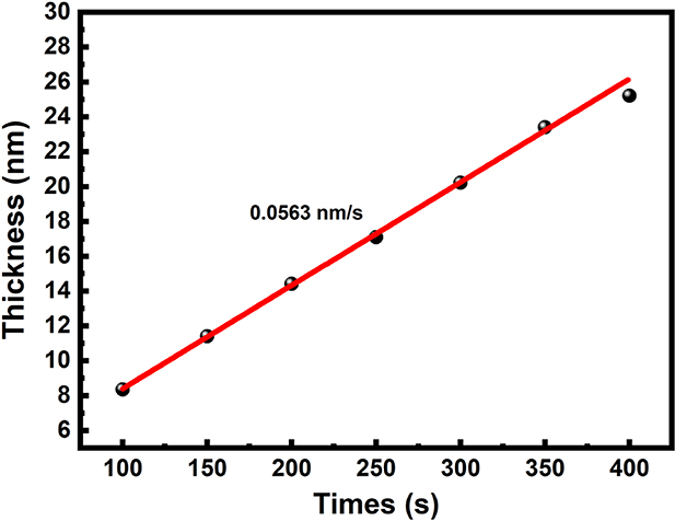
Figure 1. Thickness of the TOL as a function of oxidation time (red line is linear fit of 0.0563 nm s−1).
Download figure:
Standard image High-resolution imageTable 1. TOL and COL oxidation parameters.
| Sample | Recipe | Oxidation time |
|---|---|---|
| TOL | 900 ∘C 1000 sccm oxygen | 14 s |
| COL |

| 10–20 min |
To examine surface flatness, we performed tapping AFM imaging of the different oxidised samples compared to bare Si. As shown in figure 2, both methods produce extremely flat surfaces with RMS roughness of 1.003 nm (10 min COLs, figure 2(b)) and 0.962 nm (14 s TOL, figure 2(c)), which follows the corresponding value of the original Si(100) wafers (RMS =  nm, figure 2(a)). The surface of TOLs maintains a flatness of 1.011 nm with a thickness up to ~26 nm (400 s TOL), meaning that no undesired cluster-like oxidation is recorded through potential defects or contamination [33, 34].

Figure 2. AFM images of the (a) Si, (b) 10 min COL (2 nm), (c)14 s TOL (~1 nm), and (d) 400 s TOL (26 nm).
Download figure:
Standard image High-resolution imageThermal deoxidation does not involve any reducing agent such as hydrogen, which was proved to be a defect for InAs materials [35]. It is performed with the MBE by the following reaction,

where the SiO is gaseous and will be desorbed from the substrate under high temperature, leaving a pure Si surface. Though the nucleation of the inhomogeneous desorption of  is still not clear, the decomposition rate of the oxide layer can be described by an empirical time-rate limiting law, which closely relates with both temperature and time [36]. Therefore, we increased the deoxidation temperature in our MBE to 1000 ∘C to minimize the process time. As shown in figure 3(a), residual
  islands can be observed after deoxidising the 14 s TOL wafer at 1000 ∘C for 30 min. These islands have a density of 1.37 × 108 cm−2, and measure up to 25 nm in height and ~500 nm in diameter. In contrast, residual
  islands on the deoxidised 20 min COL wafer exhibit a density of 4.78 × 108 cm−2, with a much smaller profile of
  100 nm in width and 10 nm in height. Comparing our fabrication methods, the COL area coverage ratio (area of residual oxides over the whole area) is seven times lower than for TOL, while the island height is reduced by half. From this we conclude that the COL is a more promising candidate than TOL to work as a thermo-removable protecting layer. The deoxidation of the COLs were then examined by changing the oxidation time from 20 min down to 10 min under 1000 ∘C for half an hour. From the AFM observation, the sizes of the residual oxide islands are the same for all the samples while the density decreases. As shown in the inset of figure S3(a), the density decreases 1.7 times by reducing the oxidation time from 20 to 10 min. Given the minimum thickness (~1 nm) of oxide layer required to protect from natural oxidation in air, the oxidation time is limited to 10 min in our work. According to a recent report, the deoxidised area R at a fixed temperature can be described as [37],
where α and β are temperature-related constants and tn is the nucleation time of the first void. Obviously, it is critical to increase the time for the deoxidation with a fixed temperature. The oxide islands are completely removed by extending the deoxidation time from 30 min to 60 min according to equation (2), leaving a root-mean-square surface roughness of 0.312 nm, as shown in figure 3(c). Though occasional residual dots are observed, the area without islands is atomically flat and ready for epitaxial growth (figure 3(d)).
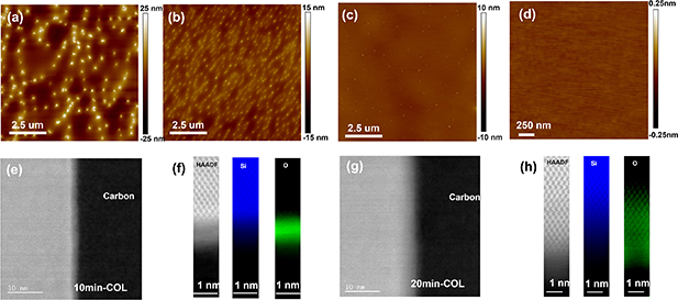
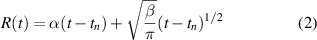
Figure 3. AFM images of the (a) deoxidised 14 s TOL wafer, (b) deoxidised 10 min COL wafer (0.5 h at 1000 ∘C), (c) deoxidised COL (1 h at 1000 ∘C), (d) high-resolution scan in island-free area, (e) and (g) HR-STEM HAADF cross-sectional images of 10 min and 20 min COLs. The crystalline substrate and COLs were protected by a carbon layer deposited during the focused-ion-beam sample preparation process, as labelled; (f) and (h) HAADF (grey) and EELS maps across the COLs for Si and C (false-colored) images of 10 min and 20 min COLs. (The intensity scale for the Si maps corresponds to 0:1 relative Si content as quantified using a model-based approach. The O map in (g) also corresponds to a 0:1 scale, whereas in (h) the O relative content is lower and displayed here on a 0:0.3 scale.)
Download figure:
Standard image High-resolution imageIn order to provide insights into the oxidation and deoxidation processes, we investigated the nature of COLs obtained with oxidation times of 20 min and 10 min prior to deoxidation by cross-sectional observation through STEM and EELS. As shown in figures 3(e) and (f), the 10 min COL exhibits a clear boundary at  interface (In contrast to
  as reported in [13]), with the extent of the amorphous oxidised region confined within a thickness of 2.1 nm above the crystalline Si (see also figure S4), with high O content (the quantification of the EELS data reveals an approximate 1:1 Si to O ratio in the amorphous oxidised layer). This observation suggests that the 10 min COL can work as a surface protecting layer by stopping any further oxidation process in air. In clear contrast, the 20 min COL sample exhibits a much wider oxidised region, with oxidation not confined to a sharply defined amorphous layer and still present at clearly detectable levels several nm (
 5 nm) below the crystalline Si surface, albeit at relatively low O content (an approximate quantification of the EELS data suggests a maximum Si:O ratio of 8:1 in this region). An amorphous layer is still visible above the surface, but narrower than in the 20 min case.(figures 3(g) and (h)). This fundamental difference in the COLs not observed before would lead to different deoxidation results.
Ge epitaxial growth was performed in the MBE with a temperature of ~1000 ∘C using previously established parameters [38]. As shown in figure 4(a), the 300 nm Ge film grown on deoxidised COL has an RMS roughness  1 nm with a low TDD of 3.33 × 108 cm−2 determined by ECCI measurements as shown in figure 4(b), compared with
  7.6 × 108 cm−2 of Ge grown on deoxidised NOL (Ge-on-De/NOL, reference sample used in this work) [38]. The XRD curve in
  mode along Ge(004) plane is shown in figure 4(c). A sharp and symmetric peak with a full width at half maximum of 391.1 arcsec implies a high crystal quality in the epitaxial Ge layer. For a strain-free (bulk) Ge layer, the peak is calculated to be 5649 arcsec from Si according to Cu
  (λ = 1.5406 Å) radiation and Bragg's law. The peaks at 5368 (Ge-on-De/COL) and 5327 arcsec (Ge-on-De/NOL) indicate bi-axial tensile stain in both samples [39, 40]. Such a strained film with a low TDD is suitable for high-quality III–V epitaxial growth [41].
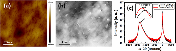
Figure 4. (a) AFM image of the Ge(100) film grown on deoxidised COL wafer, (b) ECCI image of Ge(100)-on-De/COL, (c) XRD  rocking curve the Ge(100) and the reference sample (Ge-on-De/NOL); inset is the magnified area near the Ge peaks.
Download figure:
Standard image High-resolution imageThe epitaxial Ge(100) layers were further examined by µ-Raman in order to have a deeper insight into the crystal quality. Figure 5(a) shows the spectra of the Ge(100) films used in figure 4. Except for the Ge–Ge and Si–Si signals at ~300 cm−1 and ~520.5 cm−1, the peak at ~400 cm−1 is attributed to Si–Ge from the interface. In addition, a broad peak at 2800 cm−1 was observed on both Ge wafers from residual oxides [42]. Figure 5(b) is the zoomed-in Ge–Ge signal of figure 5(a). The peak positions of the Ge-on-De/COL and Ge-on-De/NOL are at 297.7 cm−1 and 297.5 cm−1 respectively, corresponding to a shift of 1 cm−1 and 1.2 cm−1 with respect to the bulk Ge substrate measured at 298.7 cm−1 (not shown). From Raman spectra, the tensile strain  can be quantitatively evaluated from the blue-shift of the peak as,

where  is the shift of the peak, and b (= 415 ± 40 cm−1) a constant [43, 44]. From equation (3), the calculated bi-axial tensile strain is ~0.24% for the Ge-on-De/NOL and ~0.29% for the Ge-on-De/COL. The differences in the strain status are attributed to the different thermal treatments required for the deoxidation processes, and the potential residual oxides.
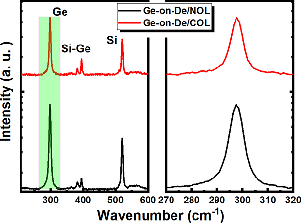
Figure 5. (a) Raman spectra of Ge-on-De/COL and Ge-on-De/NOL samples used in figure 4(b), (b) zoom-in spectra of the Ge–Ge signal in the highlighted area in (a).
Download figure:
Standard image High-resolution imageIt is known that the energy band structure of Ge is strongly related to strain, which directly affects the optoelectronic properties. As schematically shown in figure 6(a), the energy gap at the Γ point ( transition) in momentum space decreases more drastically with tensile strain than that of
  . Specifically, the minimum of the electronic valley decreases while the maximum of the light hole (
 ) band increases [45], enabling band gap engineering of Ge for high-speed detectors and light sources [17–20]. When the bi-axial tensile strain exceeds 2%, a direct bandgap can be expected. The value of
  can be obtained from the Tauc plot in figure 6(b) by extrapolating the curve at the direct transition point. We get
  values of 0.783 eV for Ge-on-De/COL and 0.772 eV for the Ge-on-De/NOL, which agrees with the calculated values from strain (0.783 eV and 0.779 eV) according to former reports [46, 47]. In addition, the non-deteriorated absorption coefficient of Ge-on-De/COL shown in figure 4(b) indicates that COLs can work as a surface protection layer for epitaxial growth on Si.

Figure 6. (a) Schematic of Ge energy band structure without (top panel) and with (bottom panel) tensile strain, (b) Tauc plot of the epitaxial Ge-on-De/COL (red) and the Ge-on-De/NOL samples (black).
Download figure:
Standard image High-resolution image
For a direct comparison, table 2 summarises our observed properties of Ge-on-De/COL and Ge-on-De/NOL. Finally, while realizing and fully characterizing a direct bandgap epitaxial Ge film is beyond the scope of this work, these findings are promising for future integration of III–V sources and high-speed strained Ge devices with prescribed optical properties in a single growth process, which is of great importance for Si photonics.
Table 2. Properties of Ge growth on De/COL and De/NOL wafers.
| Sample | Deoxidation | TDD (cm−2) |
 (arcsec) (arcsec) | Strain |
 (eV) (eV) |
|---|---|---|---|---|---|
| Ge-on-De/COL | 1000 ∘C, 1 h | 3.32 × 10⁸ | 5368 | ~0.29% | 0.783 |
| Ge-on-De/NOL |
 7.6 × 10⁸ 7.6 × 10⁸
| 5327 | ~0.24% | 0.772 |
3.1. Conclusion
In summary, we have demonstrated that  layers fabricated by a chemical method based on a mixture of
  and acidic solution provide a superior surface protecting layer on Si. Compared with TOLs, this
  layer can be thermally removed by deoxidising at 1000 ∘C. In addition, the oxidation and deoxidation processes in this work are controllable and repeatable compared with NOLs. These are crucial for ultra-clean MBE growth. As a demonstration, Ge(100) were grown on the deoxidised COL wafers. The epilayer exhibits an extremely flat surface with RMS roughness below 1 nm and an ultra-low TDD down to 3.33 × 108 cm−2 from AFM measurements. A bi-axial tensile strain of 0.24% can be confirmed from XRD and Raman characterizations, leading to a reduced band energy of 0.783 eV observed from the optical experiments. Although the experiments in this work are based on planar substrates, we believe that the ultra-thin COLs are also applicable in patterned Si substrates, such as V-grooved substrates for selective area growth and aspect ratio trapping techniques to reduce anti-phase defects and TDDs [48, 49]. Finally, our results show that high-quality Ge with tensile strain can be obtained on the deoxidised COL wafer, which is extremely useful for III/V-on-Si photonic integration as well as for high-speed Ge based devices.
Acknowledgments
The authors are grateful for support from the UKRI-EPSRC Programme Grant 'QUantum Dot On Silicon systems for communications, information processing and sensing (QUDOS)'. Electron microscopy experiments were carried out at SuperSTEM, the National Research Facility for Advanced Electron Microscopy, also supported by UKRI-EPSRC. For the purpose of open access, the author has applied a Creative Commons Attribution* (CCBY) licence to any Author Accepted Manuscript version arising.
Data availability statement
The data that support the findings of this study are available from the corresponding author upon reasonable request.
Conflict of interest
The authors declare no competing financial interest.
Supplementary data (0.5 MB PDF)