

Abstract
In the last years, the development of new materials as well as advanced fabrication techniques have enabled the transformation of electronics from bulky rigid structures into unobtrusive soft systems. This gave rise to new thin-film devices realized on previously incompatible and unconventional substrates, such as temperature-sensitive polymers, rough organic materials or fabrics. Consequently, it is now possible to realize thin-film structures on active substrates which provide additional functionality. Examples include stiffness gradients to match mechanical properties, mechanical actuation to realize smart grippers and soft robots, or microfluidic channels for lab-on-chip applications. Composite or microstructured substrates can be designed to have bespoke electrical, mechanical, biological and chemical features making the substrate an active part of a system. Here, the latest developments of smart structures carrying thin-film electronics are reviewed. Whereby the focus lies on soft and flexible systems, designed to fulfill tasks, not achievable by electronics or the substrate alone. After a brief introduction and definition of the requirements and topic areas, the materials for substrates and thin-film devices are covered with an emphasis on their intrinsic properties. Next, the technologies for electronics and substrates fabrication are summarized. Then, the desired properties and design strategies of various active substrate are discussed and benchmarked against the current state-of-the-art. Finally, available demonstrations, and use cases are presented. The review concludes by mapping the available technologies to innovative applications, identifying promising underdeveloped fields of research and potential future progress.
Export citation and abstract BibTeX RIS

Original content from this work may be used under the terms of the Creative Commons Attribution 4.0 license. Any further distribution of this work must maintain attribution to the author(s) and the title of the work, journal citation and DOI.
1. Introduction
The performance of modern electronic systems is linked to many parameters which can be used to optimize the characteristics of a system towards certain specialized applications. Nanoscale structures [1], high-mobility semiconductors [2], high-k [3] or other advanced dielectrics [4] and novel device geometries, such as FIN-FETs [5], have significantly pushed speed, complexity and power efficiency of integrated circuits. On one hand, thin-film technologies [6] have allowed the fabrication of large-scale and cheap displays [7, 8] as well as sensor arrays [9]. In parallel, novel high-bandgap semiconductors have led to high power devices [10], enabling the management of green power grids of the future. Most of these developments resulted in impressive outcomes by utilizing new processes [11], materials [12], or device structures [13–15]. Complementing these traditional approaches are electronic systems in which the overall performance is determined by the properties of unconventional substrates. These developments already started well over 50 years ago when Tellurium based transistors were fabricated for the first time on flexible polymers and paper substrates [16]. However, only the recent development of high-performance semiconductors, including organic polymers [17] as well as small molecules [18], poly-crystalline silicon [19], electronic oxides [20] and 2-dimensional (2D) materials [21], allowed the wide use of temperature sensitive materials substrates. This resulted in fully bendable active and passive devices [22], transducers [23], batteries [24], digital/analog circuits [25], and even fully integrated microprocessors [26], sensor systems [27], commercial mobile phones with foldable displays and unobtrusive wearables [28]. Potentially even more important than the demonstration of such devices is the associated possibility to manufacture thin-film systems on a wide variety of substrate materials and geometries [29]. This in turn, is essential for the ongoing trend to fabricate thin-film devices on bespoke substrates with unique features. New materials e.g. hydrogels [30], fabrication techniques such as 3D printing [31], heterogeneous multi-material substrates and functional composites can guide the customization of substrates with tailored properties: tunable Young's modulus for stretchable systems [32], transparency for invisible electronics [33], biocompatibility for degradable devices [34], or even mechanically-active structures capable to move and generate forces upon external stimuli [35], are few examples. The resulting new applications include: edible [36], compostable and environmentally-friendly devices [37], sentient robots [38], smart textiles [39], or epidermal and implantable medical devices [40]. This will open up a new chapter in the development of customised electronic systems for consumers [41], virtual reality [42], smart agriculture [43], Industry 4.0 [44], or intelligent healthcare devices [45].
The goal of this review is to outline the most prominent outcomes of electronic systems on unconventional substrate materials. First, a comprehensive analysis of materials used to fabricate substrates is presented, including mechanical, chemical, and biological properties. Then, materials employed for electronics alongside their performance are addressed. Next, technologies for electronics fabrication and structuring, and methods for designing and manufacturing substrates are discussed. In addition to the traditional role of carriers, mechanically actuated substrates, microfluidic systems, metamaterials and transparent systems are presented, followed by a discussion on engineered substrates designing, such as composites, microstructured and 3D substrates. Later, the integration of thin-film devices with the active functionality of the substrate is described. Biomedical devices, advanced agriculture systems, robotics actuators and platforms, metamaterials for terahertz applications, and smart textiles are covered. Finally, limitations, challenges, and future perspectives, and potential research directions are discussed.
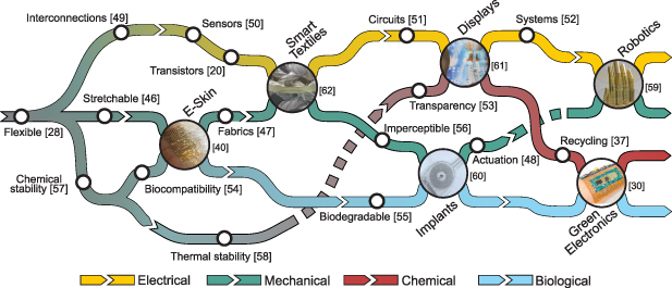
Figure 1. Visualization of the different mechanical, electrical, chemical and biological capabilities of advanced functionalized substrates. In particular the combination of different characteristics [20, 28, 37, 46–58] can lead to innovative applications [30, 40, 59–62]. Pictures [30, 40, 59–62] reproduced with permission.
Download figure:
Standard image High-resolution image1.1. Relevant performance parameters
In contrast to conventional electronics which mostly focus on electrical performance, heat management and commercial aspects, electronic systems on active substrates have to satisfy a wider but also more specialized set of requirements. Important performance indicators are:
1.1.1. Electrical.
The electrical properties of electronics on unconventional substrates are less relevant than for standard electronics, but are still of paramount importance for the functionality of a system. As in conventional electronics, they include the mobility [63], speed [64], and operation voltages [65] of transistors, the complexity [25], gain [66], and noise performance [67] of integrated circuits [68], the sensitivity and accuracy of sensors [69], and the power consumption [3] of the thin-film systems itself. Additionally, the potential electrical functionality of the substrate has to be taken into account. These include stretchable and bendable interconnections [70], the dielectric properties [71] and transparency [53] of the mechanical support, and sometimes the substrate even is a part of the thin-film device itself e.g. by acting as the gate dielectric of thin-film transistors (TFTs) [72].
1.1.2. Mechanical.
With the possibility to explore new fields of applications, unachievable for standard rigid electronics, the mechanical properties of these systems are a key factor. First of all, robustness [73], during fabrication and under normal usage conditions, guarantees system stability and proper functionality. This implies resistance to a variation of the environmental conditions (temperature and humidity) and mechanical loads [74]. Intrinsic mechanical properties, such as Young's modulus, strength, resilience, ductility, and rigidity, provide indications on which application could be tackled. As a result, the minimum bending radius [75], maximum stretching strain [76] and conformability [56] to the target surface are significant.
1.1.3. Chemical and biological.
Similarly to mechanical properties, these features are essential for unconventional systems. Chemical resistance to both reagents and harsh environments [58] are crucial, for fabrication protocols and final usage purposes. Material composition [77], in combination with biocompatibility [78], are of paramount importance, while aiming for green and dissolvable devices [79], implantable systems and edible electronics [80, 81].
2. Materials
An overview of the materials used as a substrates and employed in thin-film fabrication is presented. Section 2.1 is devoted to the materials for substrates and section 2.2 introduces the materials for electronics according to relevant electronics parameters.
2.1. Active substrate materials
The following discussion on substrate materials is based on their compatibility with electronics fabrication process and their ability to provide active properties like mechanical actuation, extreme bendability, transience, and shape memory behavior.
2.1.1. Mechanically flexible supports.
Polymers define a broad range of materials. Their mechanical flexibility is attractive for the possibility to have stable thin-film electronics performance on non-flat surfaces. Imperceptible and conformable electronics are achieved by ultra-thin, lightweight, and transparent polymers [53, 82–84]. Stimuli-responsive materials like hydrogels and shape memory polymers or stretchable polymers, such as elastomers, can further improve the electronic's mechanical adaption [46, 85–90]. Polymeric substrates can be electrically active due to percolation pathways of particles in the elastomeric matrix [91], or a conductive filler dispersion such as carbon black [92] or poly(3,4-ethylenedioxythiophene) polystyrene sulfonate (PEDOT:PSS) [93].
Degradable, bioresorbable, and biocompatible active polymers have been pointed out for green, recyclable, and flexible electronics [54, 55, 79, 88, 94]. All these properties are fundamental for wearable devices [92, 95–97], on-skin monitoring system [46, 88, 91, 98], and soft robotic applications [23, 99, 100].
Polyimide (PI) is the most common employed substrate for flexible thin-film electronics with a thickness ranging from ≈1.5 µm to ≈50 µm [23, 48, 52, 68, 83, 92, 95, 96, 98, 101–113]. PI foils are commercially available [95, 106] alternatively membranes can be spin-coated on a temporary carrier [48, 83, 110]. Its thermal stability is characterized by a low thermal expansion coefficient of 3.4 ppm ∘C−1 and a high glass transition of 360 ∘C−1 temperature [107] allowing processing temperatures up to ≈300 ∘C−1 [83]. These properties and their chemical stability make it suitable for thin-film fabrication techniques (sections 3.1 and 3.2) involving standard photolithography processes, lift-off, and wet-etching [104, 105, 108]. Its natural flexibility, as shown in figure 2(a) ensures functionality under variable bending conditions: for 50 µm thick PI a minimum bending radius of 1.7 mm was achieved [103]. This can be further reduced to 125 µm [101] through neutral strain plane designs, as described in section 4.6. Despite ultra-thin PI layer showing a transparency of 90% [83], PI is generally characterized by an amber colour, which makes other polymers more suitable for transparent electronics. These include parylene [53, 82, 84, 99, 114, 115], polyethylene terephthalate (PET) [41, 98, 116–120], polyethylene naphthalate (PEN) [92, 121], and polymethyl methacrylate (PMMA) [29, 122].
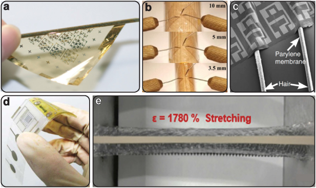
Figure 2. Mechanically flexible substrates. (a) Flexible polyimide substrate wrapped around a cylinder with a radius of 300 µm [102]. (b) A transparent 10 µm thick parylene substrate bent on wood sticks with scaling radius [82]. (c) A parylene membrane is wrapped hairs with a radius of 50 µm [53]. (d) Epidermal system on flexible PET and PI substrate [98]. (e) Highly stretchable hydrogel-ecoflex bilayer can be elongated up to 1780% of strain [46].
Download figure:
Standard image High-resolution imageParylene is a flexible and transparent polymer acting as a substrate or as insulating layer (figure 2(b)). Tens of micrometer-thick substrates [82, 114], as well as ultra-thin membranes around 1 µm are obtained by evaporation process [53, 84, 99, 115]. Due to this low thickness, thin-film electronics fabrication must be performed while depositing the polymer on a rigid carrier covered by a sacrificial layer [53, 84, 115]. Thin-film electronics fabricated on parylene is bent down to 50 µm as shown in figure 2(c). The minimum bending radius decreased by decreasing the strain induced by bending a 1 µm-thick substrate [53]. Similarly, PEN foils (generally 50 µm thick), as well as, PET foils with a thickness ranging from 1.4 µm [118] up to 175 µm [116] are commercially available. Their flexibility is beneficial for the conformability of epidermal electronics [98, 118] (figure 2(d)) or smart textile applications [41, 92].
PMMA is a transparent and flexible polymer that can act as substrate [29, 122] and dielectric layer [120, 123, 124]. Thin-film transistors on micrometer-thick PMMA ( 2 µm) showed stable electronics performance when cycling bending test at a minimum bending radius of 1 mm was performed [122]. As with other solution-based polymers, the electronics fabrication can be carried out by spin coating the PMMA on rigid support. Free-standing devices on PMMA substrate are obtained through transfer printing process as described in section 3.6. Moreover, PMMA itself acts as sacrificial layer enabling free-standing electronics on other polymeric substrates thanks to its solubility in organic solvents [125–127].
Rubbery elastomers such as polydimethylsiloxane (PDMS) [49, 51, 83, 85, 86, 91, 99, 100, 110, 128–139] and Ecoflex [46, 88, 137, 140–142] are mainly attractive for their stretchability that is missing in other plastic materials. These features are particularly beneficial for wearable and epidermal patches [46, 88, 91, 142]. PDMS is characterized by a low Young's modulus of ≈2 MPa [49, 134]. The stretchability of PDMS, acting as active substrate, depends on both the elastomer deposition and design. Casting deposited PDMS was strained up to 5% [49, 86], but a maximum applied strain of 20% was achieved when an 800 µm thick pillars' mould was exploited [133]. This geometry allowed a twisting of the substrate up to 180∘. Spin-coated PDMS swells during the curing process due to its high thermal expansion coefficient of  K−1 [128]. Constrained deformation of PDMS is achieved by depositing it on material with lower thermal expansion coefficient enabling the fabrication of thermal PDMS soft actuators [99, 110] or electronics on non-flat surfaces for skin applications [51]. Other strategies to take advantage of the PDMS stretchability involve engineered strain distribution and are described in section 4.6. PDMS is also transparent [49, 51, 83]. Ecoflex is transparent, commercially available, natural, and biodegradable [88, 140] and its low Young's modulus of 0.69 Pa ensures a stretchability
  100% [46].
Biodegradable and wast-free flexible electronics can be achieved by using cellulose-based substrates that also bring the advantages of being cheap and largely available [79, 94]. Depending on the production process, it can exhibit chemical stability and a glass transition temperature  180 ∘C suitable for direct fabrication [79] or transfer printing processes [94]. Less than 5% of variation on the characteristic curve of electronics circuits is observed when cellulose is bent down to 2 mm [79]. Another example of a bio-substrate is keratin extracted from human hair [143]. Uniform layers of keratin were spin-coated on a Si carrier acting as substrate or gate dielectric. A bending test at a radius of 20 mm was performed to prove the flexibility. Additionally, a transient behaviour was showed when exposed to alkine-solution. Polypropylene based paper offers another approach for eco-friendly electronics [144]. Its thermal and chemical stability is suitable for direct thin-film fabrication while the paper is laminated on a rigid support. After releasing, the bending test was performed while the electronics functionality was preserved proving the potential paper suitability as flexible eco-substrate. Thin-film electronics on parylene membrane transferred on 100 µm thick polypropylene foil showed improved mechanical properties [53, 84]. The poor adhesion between the two polymers reduced the strain on the electronics allowing its functionality under several crumbling of the substrate [53] or an increase of the maximum stretchability [84]. Polypropylene is also employed in form of natural and lightweight fibers suitable for smart textile [145, 146].
2.1.2. Shape memory materials.
Shape memory materials are a unique class of materials that presents the ability to change the shape upon the application of external stimuli (e.g. temperature [147–149], magnetic field [150, 151], and chemical conditions [152, 153]). In a macroscopic point of view [154], this effect has been verified in diverse materials, such as metal alloys [147, 155, 156], ceramics [157, 158], and polymers [50, 90, 159–167]. They have been extensively used in applications ranging from medical [90, 154, 168–171] to aerospace engineering [147, 172, 173]. Recently, one of the most promising applications is the use of shape memory polymers with flexible electronics [159–164, 166] and sensors [50], in which they are mainly used as substrates.
Many shape memory polymers have been used as substrates [174], such as cross-linked shape memory polyacrylate [175], which has been used as a substrate for light-emitting diodes when combined with silver nanowires or single-walled carbon nanotubes; polycaprolactone (PCL) [176], which was used to create a structure responsive to heat; and also poly(tert-butyacrylate) (PTBA) [167], which has been applied in active tactile displays. However, thiol-ene/acrylate [177] is one of the most used shape memory polymers as substrate for thin-film and commercial electronics [90, 163, 165], such as electrodes [160], OLEDS [161], capacitors [162], sensors [50], and TFTs [163, 164]. Moreover, robust and reliable process can be used to fabricate electronics onto this material. For example, pentacene organic thin-film transistors (OTFTs) were fully structured by photolithography in an array distribution pattern [163] (figure 3(a)). The OTFTs' performance was similar to the ones realized on rigid substrates fabricated with shadow mask processes, even after going through 100 bending cycles. Similarly, OTFTs can also be fabricated onto the thiol-ene/acrylate using low-temperature solution-processing, enabling high-performance OTFTs [164]. 3D e-whiskers were developed using thiol-ene/acrylates as substrate to receive multi-stimuli at the same time (figure 3(b)) [50]. Gold strain-gauges were photolithographed on the substrate and laser cutting was used for the outer perimeter of the whiskers (figures 3(c) and (d)). The device was able to map delicate surfaces, such as fingerprints, with results similar to profilometers (figure 3(e)). Additionally, thiol-ene/acrylate can be used as an insulator [162].

Figure 3. Shape memory polymers and thin film electronics. (a) A bent shape memory substrate with and a close-up view of one of the TFTs in the array [163]. (b) Demonstration of the sensing capabilities of the SMP-based sensor [50]. (c) Micrograph of the whiskers [50]. (d) Close-up view of the sensors [50]. (e) Fingerprint obtained with the SMP-based sensor [50]. Pictures reproduced with permission.
Download figure:
Standard image High-resolution image2.1.3. Transient substrates.
During the last decade, the interest in degradable electronics has been growing to address the exigency in reducing electronics waste, usually involving toxic, long-decomposable, and rare materials [140, 143, 178–180]. Research focused on bioresorbable and biodegradable materials to meet the requirements for smart medical implants (section 5.1.2), avoiding secondary surgery procedure, tissues inflammation, and enhancing the post-operative recovery [54, 55, 60, 115, 181–184], and favouring a sustainable approach for electronics fabrication. In this view, substrate materials and strategies for so-called transient electronics that can be dissolved are presented in the following.
Polyvinyl alcohol (PVA) is a water-soluble transparent polymer that can be used as substrate for transient electronics [185–187]. The PVA dissolution time in deionized water is around 30 min [186, 187], but it depends on many parameters such as thickness of the layer, water temperature, and post-deposition treatment [126]. Liquid metal patterned on PVA was completely recollected after polymer dissolution, proving its suitable for fully recyclable systems [185]. Shadow mask patterning [126] or transfer printing process [186, 187], as described in sections 3.3 and 3.2, are generally preferred for PVA.
Poly-anhydrides constitute a class of polymers suitable for transient electronics [183, 188–190]. Acid compounds by-products following their dissolution in water enhance the degradation of no-transient metals [188]. Their dissolution time depends on temperature, pH, and chemical composition [189, 190]. A 120 µm thick layer showed a dissolution rate of 1.3 µm d−1 [183] suggesting the suitability of poly-anhydrides as encapsulation layer for electronics and biomedical implants [183, 190].
Poly lactic-co-glycolic acid (PLGA) is also used as transient substrate [54, 60, 125, 183, 190]. PLGA dissolves in phosphate buffer solution (PBS) at physiological temperature (37 ∘C) over weeks (researchers reported a period from 4 to 8 weeks) and its biocompatibility makes it suitable for long-term health monitoring [54, 60, 183].
Naturally derived materials, such as cellulose [79] or silk [55, 182], are also employed for biodegradable and transient electronics as well as water-soluble and edible rice paper [125].
The electronics shut-down can be achieved by stimuli-responsive materials such as cyclic poly(phthalaldehyde) (cPPA) where UV-exposure or temperature triggers an acid molecule release leading to degradation [191, 192]. Accordingly, direct electronics fabrication involving UV-photolithography on this substrate is avoided and it is replaced with transfer printing [191] or stencil mask [192]. Devices for food packaging control are envisioned applications of this approach [193, 194].
2.1.4. Textiles substrates.
In recent years, there has been a significant interest in wearable electronics and this has lead to the integration of electronic functionality into everyday textiles [195]. Textiles have been preferred for wearable application due to it is familiarity and ability to comfortably conform onto the human body. Most of the flexible structures that are utilised in flexible electronics are unable to conform onto body shapes because they can only deform along one single dimension and often fail under twisting or other severe deformations. For this reason, effort has been devoted to employ textile fabrics and yarns as substrates when developing electronic devices [113, 196–212]. In general textile materials are washable, permeable to gases or liquids, able to withstand even severe mechanical deformations such as folding or sheering and in some cases they are also stretchable. These features make textiles a desirable substrate for thin-film electronics and highly suitable for smart textile and wearable applications (section 5.5).
Researchers have utilised knitted or woven textile fabrics as substrates [197, 199–201, 204, 209, 211–213]. These fabrics were made from both natural fibers and synthetic fibers such as cotton [209, 211], polyester [201, 209], meta-aramid [201], nylon [199–201, 212, 213], glass fiber [197], kermel [209], polyurethane [212], elastene [213], polypropylene [145, 146], and silk [210]. The devices fabricated on the textile include electrodes [199, 201, 212], resistors [200], transistors [204], sensors [213], solar cells [197], piezoelectric fabrics [209] and thermoelectric nanogenerators [211].
Textile threads and fibres were also used as substrates to fabricate thin film electronic devices [113, 196, 198, 202, 203, 205–208, 214]. Textile fibres are the raw materials for manufacturing textile fabrics. In some cases, electronic devices were built directly on the textile fibres and yarns [113, 196, 205–207], whereas in others these fibres were utilised within a textile structure to create an electronic device [198, 202, 203, 207, 208, 214]. The most commonly used fibre is nylon [113, 196, 202, 214] but researchers have also utilised Kevlar multifilament [203], PET fibres [198], silk [207], glass fibre [196], acrylic [205] and linen [206]. Devices fabricated using these functional fibres include sensors [113, 198, 207], transistors [196, 202, 203, 205, 206] and piezoelectric generators [208].
Table 1. Thin-film devices and their performances for the active substrates described in section 2.1. Each row underlines the best example, among the reviewed ones, for a specific property.
| Substrate material and thickness | Devices | Electronics performance | Mechanical properties | Features | Reference |
|---|---|---|---|---|---|
| Parylene 1 µm | TFT |
µ = 11.3 cm2 V−1 s−1 V = 0.4 V SS = 180 mV dec−1 = 0.4 V SS = 180 mV dec−1

| Max. strain: 210% | Biocompatible | [84] |
| PMDS 80 µm | TFT, logic, circuits and rectifiers |
µ = 13.7 cm2 V−1 s−1 V = 0.1 V SS = 130 mV dec−1 = 0.1 V SS = 130 mV dec−1

| Bending radius: 13 µm | Biocompatible and imperceptible | [51] |
| Cellulose 800 µm | TFT, logic and circuits |
µ = 0.12 cm2 V−1 s−1 V = 5.75 V = 5.75 V 
| Bending radius: 2 mm | Green and biocompatible | [79] |
| PLGA 30 µm | TFTs and array |
µ = 200 cm2 V−1 s−1 V = 1 V = 1 V 
| Bending radius: 1 mm | Transient and bioresorbable | [54] |
| Polypropylene 30 µm | Capacitive + resistive touch display and LED display | Rise and fall time: 1.4 ms, emission peak at 500 nm | Bending radius: 10 mm and repeated torsion:  1000 cycles 1000 cycles | Transparent | [146] |
| Silk worm fiber | Temperature and pressure sensors | Temperature sensitivity:  C−1, pressure sensitivity: 0.136 kPa−1 C−1, pressure sensitivity: 0.136 kPa−1
| Bending angle: 0∘–360∘ | Biocompatible and washable (3 × washing machine with detergent) | [207] |
| Gold microfiber 100 µm | TFTs | V = −1.01 V = −1.01 V 
| Bending radius: 2.0 mm | Washable (beaker with detergent) | [142] |
| Thiolene/Acrylate 50 µm | OTFT | V = −7 V µ = 0.018 cm2 V−1 s−1 = −7 V µ = 0.018 cm2 V−1 s−1
| Bending radius: 8.5 mm (100 cycles) | Recovareble after deformation | [163] |
When developing thin-film structures on textile substrates it is vital to consider the impact of bending, sheer and twisting of the textile structure on the performance of the fabricated device. Furthermore, the literature illustrates that the surface roughness of textile yarns and fabrics have also had an impact on the device performance [113, 196, 201]. To reduce the influence of surface roughness researchers have employed techniques such as ultraviolet-ozone treatment [201] and coating or lamination of the textile prior to creating devices [199, 200]. Hence, surface roughness of the textile substrate and the ability of the rest of the device to withstand multi axial mechanical deformations remain as essential factors to consider when developing thin-film devices on textiles substrates.
2.1.5. Other substrates.
Thin-film structures were also fabricated on cylindrical substrates such as metal wires [47, 142, 215], glass fibers [216], and optical fibers [217–219]. These devices were mainly utilised to create transistors for electronic textile applications [142, 215, 217–219]. The high conformability of wires enables them to be used as substrates in smart textile applications. Therefore, the feasibility of synthesising devices on copper [215], gold [142] and aluminum [47] wires were evaluated. On one occasion the wire was cleaned and heated to form an oxide coating [215], whereas in others they were coated in a PDMS or P3HT solution [47, 142]. For the glass fibers, metals like chromium, copper, and gold were evaporated all around the fiber [216]. The ability of these substrates to withstand harsh environments makes them suitable for applications such as structural health monitoring of construction materials. In the case of optical fibers, metals such as chromium and AlOx were directly deposited on the fiber substrate to fabricate devices [217]. Optical fibers have been utilised for smart textiles but their limited flexibility makes them unappealing for these applications.
More exotic materials such as natural wax [220] and ultrathin insulating poly(vinyl formal) (PVF) [221], were also utilised as substrates for creating flexible electronics. The electronic devices created using these exotic materials include transistors [221] and NFC circuits [220]. In addition, the device created on PVF was able to withstand a bending radius of 0.7 µm.
2.2. Materials for thin-film electronics
In the following paragraphs, the materials commonly used in the fabrication of thin-film electronics, such as insulators, semiconductors, and conductors, are presented, together with their roles.
2.2.1. Semiconductors.
Semiconductors in thin-film electronics are employed as active layers, defining the device technology and carrier transport efficiency. Traditional semiconductors such as silicon (Si) are well-known for their high mobility and for being mechanically rigid and brittle. To employ these materials in thin-film electronics, silicon in the form of amorphous-Si (a-Si) [129, 222] or Si nanomembranes (Si NMs) [54, 55, 60, 125, 191, 192] have been used. The small mobility (less than 1 cm2 V−1 s−1) that can be achieved with a-Si TFTs represents a limitation, while Si NMs represent a better alternative because of their higher mobility ( 500 cm2 V−1 s−1) [223]. Moreover, Si NMs were largely used in transient electronics due to their fast dissolution time [125, 192]. Poly-crystalline Si shows a mobility between 50 and 100 cm2 V−1 s−1 [224, 225]. Despite the better performance of Si NMs and poly-crystalline, their fabrication processes are expensive and time-consuming [226].
Organic semiconductors have the advantages of easy and low-cost manufacturing, mainly based on solution processes (section 3.2), and room temperature processability suitable for direct fabrication on plastic, fabrics, and transient substrates. They are mostly p-type semiconductors such as pentacene [102, 123, 136, 163, 204, 227], carbon nanotubes (CNTs) [98, 186, 206, 218, 219, 228, 229], polymeric semiconductors [79, 116, 118, 143, 230, 231] among which the most reported is poly(3-hexylthiophene) (P3HT) [91, 93, 142, 204, 206, 219, 232], or naturally derive semiconductors such as indanthrene yellow G, indanthrene brilliant orange RF, and perylene diimide [140, 179]. They are lightweight and flexible due to their chemical nature, undergoing large strain up to 50% when mixed with stretchable materials like PDMS [91] or Styrene-ethylene-butylene-styrene (SEBS) [230]. Organic naturally derived semiconductors also allowed the fabrication of edible OTFT [140, 179]. Current limitations arise from the less developed n-type semiconductors and the small achievable mobility, typically  10 cm2 V−1 s−1.
Metal oxide semiconductors have been used in the last decades due to their promising properties for thin-film electronics such as the low temperature processability ensuring high quality deposition, high mobility, optical transparency, mechanical stability, and the possibility to achieve large-scale fabrication [226, 233]. They are mostly n-type, and among them, transparent amorphous indium-gallium-zinc-oxide (a-IGZO) is the most used one [51–53, 68, 82, 84, 85, 101, 103–107, 109, 128, 131, 133–135, 137, 187, 188, 234–237] showing a mobility  10 cm2 V−1 s−1 [238], large-area processability, and low deposition temperature [20]. Other n-type amorphous metal oxide are zinc-oxide (ZnO) [49, 120, 239], zinc-tin-oxide (ZTO) [112], indium-oxide (In2O3) [131, 164], while p-type amorphous metal oxide are nickel oxide (NiO) [51] and tin-oxide (SnOx
) [72].
10 cm2 V−1 s−1 [238], large-area processability, and low deposition temperature [20]. Other n-type amorphous metal oxide are zinc-oxide (ZnO) [49, 120, 239], zinc-tin-oxide (ZTO) [112], indium-oxide (In2O3) [131, 164], while p-type amorphous metal oxide are nickel oxide (NiO) [51] and tin-oxide (SnOx
) [72].
2.2.2. Insulators.
Insulating materials in thin-film electronics are employed as passivation or buffer layers, and as dieletrics. The dielectric constant and the thickness are the fundamental parameters. Good insulating properties ensure a proper isolation of components and circuits, preventing leakage current, and voltage breakdown.
Insulating materials are silicon oxide (SiOx ) [49, 54, 55, 60, 83, 88, 125, 127, 132, 186, 187, 236, 237], aluminum oxide (Al2O3) [51–53, 68, 79, 84, 101, 103, 105–109, 112, 118, 128, 131, 133, 135, 234, 235, 240], hafnium oxide (HfO) [3, 165, 228], magnesium oxide (MgO) [55, 188], silicon nitride (SiNx ) [54, 88, 129, 131, 186, 187, 236] or polymers such as parylene [86, 112, 114, 136, 163], polyimide [241, 242], SU8 [49], hydrogels, [116] and ion-gels [91, 93]. Moreover, organic dielectrics are glucose, lactose, or nucleobase [179].
SiO2 is a bioresorbable insulating material employed as electronics dielectric layer [49, 55, 60, 83, 125, 127, 236] or passivation/encapsulation layer [54, 55, 83, 88, 236]. It is deposited by plasma-enhanced chemical vapor deposition (PECVD) (section 3.1). Oxide layers ranging from 50 nm to 900 nm are water soluble [55, 125, 127], and their solubility is also proved on saline [29] and PBS [54, 60, 125] solutions. The large SiO2 layer thickness is required when it is employed as a gate dielectric layer because of its low dielectric constant, around 4. For this reason, high-k dielectric materials [243] are preferred for thin-film electronics e.g. Al2O3 exhibiting a dielectric constant of ≈8.5 [79] or HfO2 acting as gate dielectric with a thickness of 20 nm [228].
MgO is used as gate dielectric for transient thin-film electronics [191], and it can also act as passivation layer to tune the dissolution time of the transient electronics according to its thickness [55]. SiNx can be deposited as a single layer [129] or in sandwich structures with SiO2 [54, 186, 187] acting as passivation layer, gas barrier layer [83], or humidity barrier [236].
Although polymeric dielectrics have lower dielectric constant than SiO (
( = 3.24 [242],
  = 4 [244]), they are suitable as substrate for their stretchability and bendability. Parylene substrate hosting TFTs with parylene dielectric-layers can undergo up to 10 000 bending cycles [114], while hydrogel dielectric based TFTs can withstand a maximum strain of 55% [116]. Additionally, shape memory polymers can also be used as insulators providing two different dielectric constants and resistivity depending on the temperature. For example, thiol-ene/acrylate has a dielectric constant of 5.26 ± 0.11 and 6.38 ± 0.11, below and above the transition temperature, respectively [162].
Sandwich insulating structures are fabricated for improved dielectric performance due to the combination of different dielectric materials [231, 245]. Both polymers and organic dielectrics are deposited in the form of bilayer dielectric structure with Al2O3 [102, 112, 134, 140]. OTFTs based on nucleobased dielectric layers showed larger capacitance per unit of area (from 5.6 nF cm−2 to 23.4 nF cm−2) when forming a hybrid organic/inorganic with Al2O3 [140].
2.2.3. Conductors.
Most of the employed conductor materials for thin-film electronics are metals. Copper (Cu) [51, 133], gold (Au) [129, 131, 136, 234], and aluminum (Al) [86, 112, 239] are extensively used because of their high electrical conductivity of  S m−1,
  S m−1, and
  S m−1 respectively [246]. Chromium (Cr) [234, 235], and titanium (Ti) [51, 231, 241] have a low electrical conductivity, are employed as adhesive layers to improve the adhesion of other metals like Au [132, 231, 237, 241], platinum (Pt) [132, 241], palladium (Pd) [186]. However, Cr is also less ductile, showing a smaller rupture strain level (
 0.5%) compared to others, such as Cu, limiting the minimum achievable bending radius [103].
Molybdenum (Mo) [54, 83, 186, 187, 236] and magnesium (Mg) [55, 60, 88, 125] are commonly employed for their biodegradability and biocompatibility. Moreover, Mg is also water soluble and suitable for bioresorbable implants, while Mo can degrade in acid environment as zinc (Zn) or iron (Fe) [191].
Fully transparent electronics are fabricated through transparent conductive oxide such as indium-tin-oxide (ITO) [49, 51, 82, 107, 116]. However, it was shown that they easily experience fractures and delamination [53].
Metals can be deposited through vacuum-based technologies (section 3.1), some can also be solution processed (section 3.2).
Additionally, so-called liquid metals, consisting of metals and metals alloys that are liquid at room temperature, have been used for compliant and microfluidic electronics. Within this class, galinstan (GaInSn) [139, 185, 247], and eutectic gallium-indium (EGaIn) [139, 247, 248] are the most promised candidates because of their electrical conductivity of  S m−1 and low melting point equals to 19 ∘C−1 and 15.5 ∘C−1 respectively.
Finally, carbon-based conductors are also employed in thin-film electronics in the form of CNTs [207, 230] or as conductive fillers in polymeric matrix [92].
3. Technologies
The established process and novelty technologies for thin-film electronics fabrication and substrate deposition are presented in the following. Sections 3.1 and 3.2 describe vacuum-based technologies and solution-based processes for electronics fabrication, and the deposition of substrates materials. Next, in sections 3.4 and 3.5, 3D printing techniques and molding process for substrate fabrication are introduced. Finally, section 3.6 gives an overview on alternative techniques and strategies for the fabrication of electronics on unconventional substrates.
3.1. Vacuum based thin-film technology
Vacuum-based technologies can be divided into two main groups that are physical vapor deposition (PVD) and chemical vapor deposition (CVD). PVD processes, consisting of electron beam evaporation (e-beam), thermal evaporation, and sputtering, are based on the vapour condensation of a source material on the desired substrate [249]. Thermal evaporation processes exploit the current flowing on a crucible to heat the source material; whereas, e-beam evaporation relies on accelerated electrons emitted from an electron gun to evaporate or sublimate the source material. In both cases, the process, the roughness of the sample surface, the angle between the sample and the source affect the quality of the deposition The low working pressure condition (down to 10−4 Pa) prevents gaseous contamination and a high deposition rate (up to 1 µm min−1) can be achieved. Both thermal and e-beam evaporation are mainly employed for metals such as Cr [55, 68, 105, 134, 136, 223, 241], Au [55, 68, 105, 108, 116, 117, 134, 136, 223, 228, 241], Ti [68, 108, 128, 133, 228, 241], Mg [105, 125], Mo [187], Cu [128, 133, 188] and Al [112, 137]. Also semiconductors [86, 136, 188, 191, 204, 227] and dielectrics [140, 231] can be evaporated.
Sputtering processes are based on a bombardment of a source material from an ionizing injected gas. The source dimension ensured several arrival angles of the eroded atoms on the substrate allowing conformal films deposition. Both DC and RF sputtering process are used for conductive materials [51, 54, 60, 82, 88, 190, 191, 236], and semiconductors [51, 105, 128, 134, 137, 187, 188, 236], while RF sputtering must be used for insulators.
CVD process relies on chemical reactions of vapour phase reactants near or on the substrate. Different CVD process can be distinguished [250]. Among them, plasma-enhanced CVD (PECVD) exploits the formation of an ionizing gas within the chamber exciting the reactants and allowing the chemical reactions and film formation at lower temperature (below  450 ∘C−1) than other CVD processes. Fast deposition rate and good step coverage are also achieved, while unwanted contamination or damage due to plasma can be possible. It is employed for dielectrics deposition such as SiOx
[55, 60, 187, 236], and SiNx
[55, 68, 186], conductive layers [114, 251], but also polymeric substrates such as parylene [82]. Conformal deposition can be achieved by atomic layer deposition (ALD) processes whose prime feature is the control on the thickness [105, 252]. The chemical reactions on the substrate surface occurs in a sequential way allowing an atomically-thick layer-by-layer growing of smooth thin-film. Materials deposited by ALD are dielectrics such as Al2O3 [68, 79, 108, 112, 114, 128, 133, 137, 223] and HfO2 [228], or metals [222].
450 ∘C−1) than other CVD processes. Fast deposition rate and good step coverage are also achieved, while unwanted contamination or damage due to plasma can be possible. It is employed for dielectrics deposition such as SiOx
[55, 60, 187, 236], and SiNx
[55, 68, 186], conductive layers [114, 251], but also polymeric substrates such as parylene [82]. Conformal deposition can be achieved by atomic layer deposition (ALD) processes whose prime feature is the control on the thickness [105, 252]. The chemical reactions on the substrate surface occurs in a sequential way allowing an atomically-thick layer-by-layer growing of smooth thin-film. Materials deposited by ALD are dielectrics such as Al2O3 [68, 79, 108, 112, 114, 128, 133, 137, 223] and HfO2 [228], or metals [222].
3.2. Solution based processing
Solution based processing offers the possibility of low-cost large area fabrication, uniform and dense deposition for both electronics and substrate materials. Depending on how the material is deposited, different techniques can be distinguished such as coating process (spin, dip, and spray) [253], and printing technologies [254].
Spin coating consists in the spread of the material on a surface by centrifuge rotation. It is a fast process where the rotation speed can be used to control the thickness of the deposited layer. Both the speed and uniformity of the layer are affected by the viscosity of the material. Compared to other solution process, a greater material consumption occurs. The process is suitable for solution processed semiconductors [79, 93, 112, 116, 186] and insulators acting as substrate [230] or gate dielectric [143]. Polymeric materials can be also spin coated as a substrate [88, 230, 241], encapsulation layers [88] or planarization layer reducing the roughness of substrate [102]. Spin coated materials require annealing processes to remove all the solvents from the solution. Normally, thermally and chemically stable substrates like cellulose [79] and polyimide [88] are required. Alternatively, deposition and sintering steps are performed on a rigid carrier, followed by transfer printing (section 3.6) onto the desired substrate [55, 191].
During spray coating processes, solution is heated and sprayed on the substrate through a gas stream. The thickness of the deposited layer depends on how many times the spray coating is performed. Despite the material is thermally heated, the temperature of the substrate does not increase allowing the suitability of the process on different substrates. For instance, CNTs were spray coated on SEBS [230] or on fabric [210] as conductive layer, but also semiconductor [123, 201, 255] and dielectric materials can be deposited as proved in a fully spray coated solar cell [232]. Patterning of spray-coated material can be performed during the process by shadow mask.
Dip coating processes immerse the sample in a bath of the material to be deposited. After coating and drying steps are required to result in a uniform layer. As spray coating, also dip coating is a repeatable process allowing an easy adjustment of the thickness. It is also a cheap and waste-free process. It can be used for both organic [201, 218, 228, 228] and inorganic TFTs active layer [217] or as encapsulation/protective layer [215]. Roll-to-roll fabrication on textile dip coated on conductive PEDOT:PSS has been reported [203].
Printing technologies allow simultaneous deposition and patterning. Screen printing offers a fast route to define the pattern layer by ink dropping on a substrate through a mask pattern. The substrate does not undergo any thermal and chemical stress, thus the technique is suitable for elastomers [46], plastic foils [98], and textiles [209]. Inkjet printing selectively ejects a liquid ink through a nozzle on the surface followed by annealing or sintering to cure the ink. Inkjet can be used on 3D printed substrates [176, 180, 256]. Finally, gravure printing is based on rolling cylinders spreading a liquid ink on an indented substrate. The process is particularly suitable for microfluidic devices based on liquid metals [185], but also semiconductors, insulating, and metals can be employed [229].
3.3. Electronics structuring
Electronics materials deposited through vacuum technologies (section 3.1) or coating solution-based processes (section 3.2) are structured according to designed patterns to fabricate thin film-electronics. Photolithography is the most employed process [51, 53, 103, 105, 116, 117, 132, 133, 163, 257, 258]. It consists of several steps based on the use of a photosensitive compound, which is deposited on the substrate typically through a spin-coating process, and exposed to a source light, while the substrate is covered with a patterned mask. Different light sources can be employed and the wavelength is chosen according to the photoresist properties. After the exposure and depending on the photoresist, wet etching processes of the substrate in a proper developer solution are used to remove the exposed area of the photoresist (positive photolithography) or the not exposed ones (negative photolithography), leading to the pattern definition. Afterwards, the electronics materials are structured according to the obtained pattern by others wet etching steps. Although the photolithography process is compatible with many polymeric substrates, for example, polyimide [103, 105], parylene [53, 116], PET [116, 117], thiol-ene/acrylate [163], light-sensitivity or chemicals involved in wet etching processes can cause the swelling or damage of some substrates. To overcome these issues, the patterning can be performed through a shadow mask process. In this case, the mask covers the substrate during the materials deposition processes, resulting in the direct structuring of the materials while they are deposited [60, 79, 93, 129, 134, 135, 140, 143, 191]. Another alternative consists in transferring processes, as described in section 3.6.
3.4. 3D printing
3D printing has been attracting attention in many fields in science and industry, mostly because of its ability to fabricate objects of complex shape layer-by-layer with reduced waste. When it comes to fabricating substrates, the main techniques used are fuse deposition modelling (FDM) [255, 259, 260], and UV-light based techniques, which includes stereolithography (SLA) [176, 261] and digital light processing (DLP) [259, 262].
Fuse deposition modeling is used to print mechanically resistant structures through melting high-strength thermoplastics, such as nylon [263], polypropylene [264], thermoplastic polyurethane (TPU) [265], polyether ether ketone (PEEK) [266], polylactic acid (PLA) [267, 268], polyethilene [264], and acrylonitrile butadiene styrene-based materials (ABS) [255, 268, 269]. Normally, the printed surfaces are wavy with a roughness around 15 µm [255], requiring a planarization. The planarization can be carried out by using a microwave remote-plasma etcher [255], by heating the printed device and applying a flat mold on it, by exposing the printed object to acetone vapor [270], or by using spray deposition of an insulating material (figure 4(a)) resulting in a root mean square (RMS) roughness around 0.39 µm. After the planarization, conductive layers can be added onto the surface, for example, carbon nanotubes, silver nanowires, or PEDOT:PSS [255]. Figure 4(b) shows a structure printed through FDM using a semi-transparent ABS-derivative material later planarized through spray deposition of an insulating semi-transparent ABS-derivative mixed with an organic solvent.

Figure 4. 3D printing technologies. (a) Illustration of the planarization of a FDM printed structure through spray deposition of an insulating material [255]. (b) Planarized FDM printed structure [255]. (c) 3D structure printed using SLA technique. [176]. (d) 3D structure printed using DLP technique [262]. Pictures reproduced with permission.
Download figure:
Standard image High-resolution imageUV light-based 3D printing is a technique that can also be employed for building substrates [176, 261, 262, 271]. The fabrication process consists of irradiating the UV light in a liquid polymer resin containing photoinitiators, photoacid or photoradical generators [259, 260]. The light induces the decomposition of the photoinitiators and triggers the polymerization and the curing of the exposed region [176, 259, 262].
SLA [176] and DLP [262] have been employed for building substrates. In both techniques, materials such as silicone, polysiloxane-containing formulations, acrylate-based, and thiol-ene-based materials have been used to print elastomeric objects [272]. To fabricate biocompatible substrates, resin mixtures, that include macromers combined with non-reactive diluents such as N-methylpyrrolidone (NMP) or water, are alternatives [273, 274]. The structures is printed layer by layer and each layer is coated on top of the cured layer. Here, supporting materials may be necessary depending on the complexity of the structure [261]. This technique is attractive when substrates with high-resolution printing (around 50 µm) are necessary [260]. For example, the SLA technique was used to fabricate an electrical switch with shape memory polymer PCL macromonomers and metal layers for a commercial LED [176], resulting in a structure that could be switched on and off (figure 4(c)) through heating.
DLP uses UV light projection to illuminate each layer for polymerization, resulting in a shorter time when compared to stereolitographic methods [260]. This method is capable of creating very complex substrates with high precision around 10 µm. It also enables the production of hollow and porous structures, since the printing is performed in a liquid environment and does not require any supporting materials, which is an asset for the fabrication, as removing supporting materials might cause damages to delicate printed substrates [262]. For example, a complex bucky ball-shaped substrate was 3D printed with a highly stretchable material (SUV elastomer polymer resin) through the DLP technique and then used as conductive switch after being coated with silver nanoparticles [262]. It could be switched on and off through the deformation of the structure (figure 4(d)).
Despite 3D printing technologies enabling the fabrication of objects with complex shapes, the integration with thin-film electronics and sensors is still a challenge because their fabrication requires processes that are not compatible with the materials used in 3D printing techniques. Therefore, molding (section 3.5) might represent a more suitable alternative for building substrates with complex shapes [133, 275].
3.5. Molding
To fabricate substrates with high stretchability, bendability, and conformability, molding is an established technology. It relies on pouring a non-cured material in a mold so that it can be cured e.g. by UV light-based photopolymerization or heating. This method is employed for creating elastomeric substrates and consists in injecting non-cured material between two parallel structures, like microscope glass sliders, that are separated by a spacer to set the thickness and then carry out the curing process. It has been used to fabricate planar substrates [50]. For example, a 125 µm thick shape memory polymer substrate [160] was fabricated, having a electro-beam evaporated Au layer onto it. Similarly, a 1 µm thick shape memory polymer substrate was fabricated with a following addition of thermal-evaporated inverted top-emitting OLEDS [161].
Coating the parallel structures with metal before injecting or pouring the non-cured material is an straightforward way of creating metal layers during the molding process. When the substrate is separated from the mold, the metal layers are already affixed on its surface. For instance, a shape memory polymer substrate was fabricated using a monomer solution in parallel microscope glass slides, in which one of the glass slides was coated with a 100 nm of gold beforehand. The posterior UV light-based photopolymerization resulted in a substrate with a gold layer adhered onto it, ready to go through the following patterning and etching process for the fabrication of OTFTs [163].
The molding technique can also be used to fabricate engineered substrates (section 4.7), which are composed of separate parts that are later bonded. This approach could result in carriers with increased functionality. As an example, a 560 µm thick PDMS layer was spin-coated on a mold with a specific shape (squared, hexagonal, and circular) then positioned on top of a second PDMS layer and bonded on the top of a planar PDMS substrate, resulting in a substrate that can withstand stretching, bending and twisting deformations [133].
3.6. Others technologies
Alternative technologies and approaches have been proposed for electronics fabrication on unconventional substrates.
Transfer printing offers a suitable route when high deposition temperatures or chemical processes can destroy the substrate. The electronics fabrication is carried out on a rigid carrier involving one or more soluble sacrificial layers, and after its dissolution, the electronics is transfer on to the desired substrate through PDMS stamp [54, 125, 191, 222, 228], thermal tape process [108, 186, 187, 228] (figure 5(a)), water-soluble tape [88], or mechanical detachment [83, 122]. Another strategy to avoid vacuum process issues on sensitive elastomeric substrates consists in a transfer-free process [131]. The active substrate was deposited on top of electronics which were fabricated on a sacrificial layer. The elastomer adhered on the electronics remained attached to the substrate while the sacrificial layer was etched. Exploiting the dissolution of a sacrificial layer can also be beneficial for free-standing electronics on ultra-thin substrates that could not directly undergo the electronics fabrication process [29, 53], as shown in figures 5(b) and (c). Here, the substrate itself is deposited on top of the sacrificial layer on a rigid support, undergoing all the electronics fabrication process, and it is released from the carrier after dissolution. The same process was also used for micro-robots fabrication [241]. Another achievement involving the dissolution of a sacrificial layer consists in self-rolled electronics where micro-fabricated layers reshape in a micro-tubular structure due to etching of the sacrificial layer and strain engineering [234, 240, 251, 276, 277]. When the transfer involves thin-film device on textile, transfer assisted process can be used to ensure the conformability on the substrate [62]. Cilia-assisted transfer printing, represented on figure 5(d), exploits cilia at the periphery of the substrate allowing a reliable wrapping around the textile threads. Moreover, cilia serve as dampers to release stress during mechanical deformation.

Figure 5. Transfer printing. (a) Electronics transfer on PVA substrate is achieved through thermal tape process pressed onto the electronics on a sacrificial layer [187]. (b) and (c) Free-standing electronics on 1 µm thick parylene obtained by water dissolution of a sacrificial layer [53]. (d) Cilia-assisted transfer printing of ultra-thin electronics on textile. The device fabricated on a bilayer sacrificial layer is transfer on a pre-treated substrate with a PMDS solution. Repeatedly dropping the PDMS solution gradually dissolves the supportive layer. After the complete dissolution, the cilia wraps around the textile [62]. Pictures reproduced with permission.
Download figure:
Standard image High-resolution imageFinally, smart textiles carrying thin film devices were created using dedicated textile manufacturing techniques such as weaving [197, 202, 202, 215], twisting [142, 203], knitting [214], and braiding [208]. In the present-day garment supply change speed is vital for the mass production of textiles [278]. Therefore, utilising already established textile manufacturing techniques enable researchers to effectively produce smart textiles with flexible electronics.
4. Substrate properties
Substrates comprise a fundamental part in the design and building of thin-film devices. In sections 4.1–4.3, the properties of mechanically actuated substrates for microfluidic system and metamaterials are presented, respectively. Sections 4.5 and 4.6 introduce micro-fabrication strategies and composite materials for strain engineered and functionalized substrates with enhanced mechanical properties. Finally, section 4.7 discusses several approaches to obtain 3D substrates.
4.1. Mechanical actuation
Mechanical actuation in substrates for thin-film electronics consists in inducing materials to perform mechanical activities, such as grasping, handling, or moving. It can be realized through materials responsive to external stimuli, such as magnetic fields [89, 150, 151, 279, 280], temperature [99, 160–166, 241], chemicals [222], and air pressure [132].
Shape memory polymers (section 2.1.2) represents a suitable option to build substrates for mechanical actuation [161–166, 175]. The ability to be triggered by differences in temperature makes it possible to assume a specific shape [148]. It can be further exploited when combined with other materials, such as magnetic particles [89, 279], to realize structures that can also be responsive to magnetic field. For example, NdFeB microparticles mixed with thiol-ene/acrylate resulted in a substrate that could assume pre-programmed shapes when heated by a magnetic field and with temperature differences [279]. However, due to the time-depended nature of the shape memory phenomenon in polymers [89], the response of the substrate was slow, requiring around 8 s for a complete actuation. A faster, near instantaneous response was verified when NdFeB microparticles were mixed with PDMS resulting in a substrate that yielded complex patterns and shapes, like curling, buckling, and folding in a controlled manner [280] (figures 6(a)–(c)).
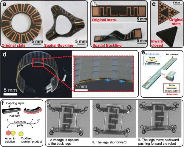
Figure 6. Mechanical actuation through external stimuli. (a)–(c) Annular, rectangular and triangular substrates assuming complex configuration upon external magnetic field [280]. (d) A PDMS substrate bends due to temperature actuation [99]. (e) Thin-film electronics (strain sensor, temperature sensor, heater) on pneumatic-controlled substrate [132]. (f)–(g) Electrochemical actuated legs. schematic of Pt-capped layer bending due to oxygen specie adsorption is shown in (f). (g) Description of the legs motion [222]. Pictures reproduced with permission.
Download figure:
Standard image High-resolution imageShape-memory behaviour, as a response to temperature variation, was used in stiff islands interconnected by shape memory alloy wires, nitinol (NiTi), on a PDMS substrate [99]. Current flowing through the actuated wires induced the shrinking and the relaxing condition of the NiTi as well as the contraction of the elastomer, leading to the bending of the whole system (figure 6(d)). No thin-film electronics was integrated, but commercial LEDs on an electrode on the surface remained functional at a bending radius of 10 mm. A thermal responsive hydrogel was also employed in a bilayer structure with an iron film to force the bending of the metal to grasp/release micro-wires [241].
Pneumatic pressure was employed as a controlling mechanism of a soft-gripper [132]. As shown in figure 6(e), the actuation was obtained by bonding a non-stretched polyimide film with a PDMS frame-layer on a pre-stretched silicon rubber. A hole was patterned on the second polyimide layer hosting the electronics and forming the air channel to allow the air-flowing. A controlled rolling around an object can be obtained down to a bending radius of 1 mm depending on the substrate thickness.
Electrochemical actuation exploiting highly reactive Pt metal films was employed for microrobot legs [222]. Capped thin-film layers of Pt electrochemically reacted in solution and bent due to species adsorption (figure 6(f)). While the legs' bending was affected by the amount of the adsorbed species, the voltage applied to the electronics on the robot body controlled their helix-curvature and actuated the movement (figure 6(g)).
Although many advancements have been achieved to build substrates that can respond to external stimuli, there are still uncovered areas. For example, thin-film electronics and sensors can benefit from the shape memory [147] and pseudoelastic phenomena [173] of thin-film shape-memory alloys [281], as these alloys can be trained [282] to assume complex shapes and are triggered by heating.
4.2. Microfluidic systems
Microfluidic systems precisely manipulate fluids in channel-like geometries at the micro scale. It has gained attention since the 80s [138], providing advancements in many research fields, such as chemistry, biology, medicine and physical sciences [283–286]. Microfluidics can be combined with electronics, for example, transistors and diodes [284, 287] and sensors [248, 285], enabling applications that would be impossible to realize using only rigid and stiff electronics devices [139].
In the design and fabrication of microfluidic devices, various elastomers have been employed, such as polystyrene [288], and poly(methyl methacrylate) [289]. However, PDMS is the most popular polymer used as substrate [139, 248, 288, 290].
When it comes to combining microfluidics with flexible electronics, conductive liquid-filled elastomeric channels can be employed to overcome the mechanical mismatch between metals (e.g. gold, copper, silver) and elastomers [84, 128]. Because of their excellent electrical conductivity, liquid metals at room temperature such as eutectic gallium-indium [139, 247, 248] and gallinstan [139, 185, 247] have been used as conductive fillers of microfluidics [290]. Furthermore, they provide reliable electrical connections in the channels even if the structure is severely deformed (figure 7(a)) [139]. Thus, conformal electronics can be built through microfluidic systems by embedding liquid conductors, electronics devices, and circuits into elastomer materials [290, 291]. Figure 7(b) shows a flexible antenna with microfluidic channels filled with galinstan that can change its properties through pneumatic inflation. The resonant frequency could vary in the range of 426–542 MHz, depending on the level of inflation [292].
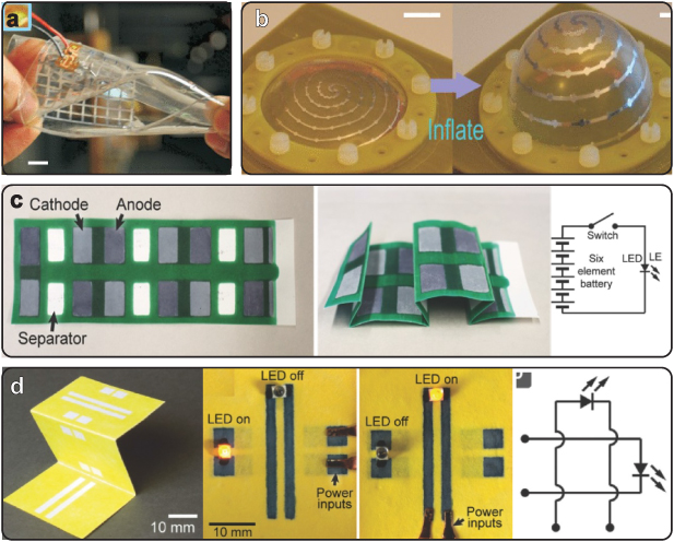
Figure 7. Microfluidic devices. (a) Severe twisting of a radio frequency sensor [286]. (b) Microfluidic based tunable spherical cap antenna at two typical working shapes [292]. (c) Battery developed using microfluidics on paper (left), battery folded (center), circuit diagram (right) [285]. (d) Wax printed channels forming a 3D circuit board (left), top view of the circuit with conductive ink (center), circuit diagram (right) [285]. Pictures reproduced with permission.
Download figure:
Standard image High-resolution imageThe fabrication of active components using the current microfluidic technology is still a challenge, as monolithic fabrication for active components represents a barrier for making fully functional microfluidic electronic systems [285]. On the other hand, hybrid integration of functional parts fabricated by many processes [138, 284, 293, 294] or materials on substrates have been used to make advanced systems [290], in which the liquid metal contacts rigid components. The strain of these advanced systems is absorbed by the elastic substrate and the rigid parts are protected, avoiding damages to the rigid parts [286] (figure 7(c)).
Monolithic integration of microfluidics and electronics on a paper was demonstrated by Hamedi et al [285]. Here, printing 2D and 3D fluidic and electrofluidic, and electrical components on a paper substrate allows the development of devices, such as printed batteries, which were able to keep a LED on for 15 s (figure 7(c)), and multilayer circuit boards (figure 7(d)).
4.3. Metamaterials
Metamaterials are a class of artificial materials exhibiting unique properties, such as acoustic [271, 295–298], and electromagnetic [299, 300] wave control, that cannot be found in nature [237, 242, 244, 271, 301, 301–306]. Essentially, metamaterials are the composition of architected unit cells with specific properties and geometries distributed along with a host structure [237, 242, 244, 271, 302–304, 307, 307–317]. The interaction between the unit cells and the host structure provides the metamaterials with their unique characteristics and functionalities [304]. Although the unit cells can be a patterned modification of the host structures [271], they are normally fabricated and then added to the host structure or fabricated directly in the host structure [237, 244, 302].
Most of the metamaterials that employ substrates and thin-film electronics are related to electromagnetic applications to manipulate waves in the range of terahertz frequencies [237, 242, 244, 307, 318, 319]. In this case, the substrate plays the role of a host structure, and the electronics, the role of the unit cells. Hence, the interaction between the electromagnetic properties of the substrate and the electronics allows the unique functionalities of these metamaterials.
In this class of materials, the substrates are fundamentally active because they can provide low electromagnetic loss [244], high response at terahertz frequency range [242], electrical conductivity, or wide band gaps [308]. Additionally, the terahertz metamaterials' substrates can also benefit from mechanical properties like stretchability, bendability, and conformability which can be provided by polymeric elastomers [242, 320].
Among many materials that can be employed as substrates for electromagnetic metamaterials, PDMS [307, 309, 318], parylene [244, 310, 311], polyimide [312, 313], and quartz [237] have been used, mostly because of their electromagnetic properties, such as the relative permittivity and the loss tangent [242].
Polyimide is the most used material for substrates in metamaterial applications. It presents a loss tangent of 0.031 between 0.2 THz and 2.5 THz [242, 312, 313]. It also provides strong adhesion to metals and mechanical stability, which facilitates fabrication [242, 315]. Parylene-based metamaterials enables devices that can withstand temperatures in the range from −200 ∘C to 200 ∘C, keeping their low-loss performance [242, 316]. It also demonstrates low-loss performance in the terahertz regime [242, 244, 310, 311], with a constant refractive index of 1.6 between 0.45 THz and 2.80 THz. In addition to being a low-cost material and the ease of fabrication, PDMS presents a permittivity of 2.35, a loss tangent of 0.04, and demonstrates a moderate dissipation across the terahertz frequency range [242, 309, 318].
Recently, cyclic olefin copolymer (COC) has gained attention because of its loss tangent of 0.0007 across the entire terahertz range (0.1–10 THz), which is three orders of magnitude lower when compared to the frequently used polymeric substrates [242, 321, 322] and enables electromagnetic devices across the entire terahertz regime [242, 317].
Although non-flexible, other materials have also been employed as substrates for electromagnetic metamaterials, such as quartz (SiO2) [237], sapphire [323], and silicon nitride (Si3Ni4) [324]. They are attractive because of their availability, low loss, high permittivity, and ease of handling [242].
4.4. Transparent substrates
For many applications, such as health monitoring systems, smart glasses, and contact lens, transparency is important [51]. To realize transparent, stretchable, and bendable substrates, PET [20, 325, 326], parylene [53, 56, 82, 115], and PDMS [51] have been used. Transparency can also be important for applications in which bendability and stretchability are not of interest. In this case, materials like PI [327] or even a mixture of polymers [328], have been exploited.
To accurately map the temperature of complex and delicate surfaces, such as fresh food (figure 8(a)), 120 nm thick PEDOT:PSSa was spray coated on top of a 1.4 µm thick PET substrate [326]. Here, the combination of PET with PEDOT:PSS endowed the device with transparency at a stretched state, while in the wrinkled stated it became translucent. In another example, an imperceptible magnetoresistive e-skin sensor was developed to endow humans with a sixth sense, detecting the presence of static and dynamic magnetic fields (figure 8(b)) [325]. Co/Cu and multilayers of Ni81Fe19/Cu were added on top of a 1.4 µm thick PET foil substrate. Besides the bendability and the good adhesion on human skin, the PET foil also ensured the imperceptibility of the device due to its transparency (figure 8(c)).
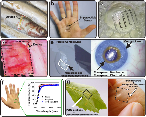
Figure 8. Transparent substrates. (a) Ultra-thin electronics monitoring the temperature of a fresh food [325]. (b) Imperceptible magnetic sensor on human-skin [325]. (c) Ultra-thin electronics on a soap bubble surface [326]. (c) Ultra-thin electronics on a soap bubble surface [325]. (d) Transparent electrophysiology array on the brain surface of an optogenetic rat [115]. (e) Transparent device transferred to a contact lens (left) and to an artificial eye (right) [53]. (f) Transmittance of devices [82]. (g) Invisible PDMS membrane with the transparent electronics on a plant leaf (left) and on a human skin (right) [51]. Pictures reproduced with permission.
Download figure:
Standard image High-resolution imageTo accurately map the temperature of complex and delicate surfaces, such as human skin or a soap bubble (figure 8(a)) or food (figure 8(c)), 120 nm thick PEDOT:PSSa was spray coated on top of a 1.4 µm thick PET substrate [325]. Here, the combination of PET with PEDOT:PSS endowed the device with transparency at a stretched state, while in the wrinkled stated it became translucent. In another example, an imperceptible magnetoresistive e-skin sensor was developed to endow humans with a sixth sense, detecting the presence of static and dynamic magnetic fields (figure 8(b)) [325]. Co/Cu and multilayers of Ni81Fe19/Cu were added on top of a 1.4 µm thick PET foil substrate. Besides the bendability and the good adhesion on human skin, the PET foil also ensured the imperceptibility of the device due to its transparency (figure 8(c)).
Parylene was used as a substrate to fabricate transparent, ultraflexible, and active multielectrodes arrays, which consisted of organic electrochemical transistors and semi-transparent Au grid wirings for local signal amplification [115]. The device was used to map electrocorticogram electrical signals, as demonstrated in figure 8(d). In another example, transparent and unobtrusive transistors and strain sensors were fabricated on top of 1 µm thick parylene [53]. Here, the substrate was transferred to a commercial polymeric contact lens, indicating a possible application in monitoring and diagnosing eye diseases, such as glaucoma (figure 8(e)). Similarly, ultra-thin transistors were deposited on top of 1 µm thick parylene to form imperceptible humidity sensors [82], achieving overall transparency of 90% (figure 8(f)).
High transparency can also be achieved through PDMS. To demonstrate the fabrication of imperceptible electronics on 3D surfaces, such as leaves or human skin (figure 8(g)), PDMS was used as a substrate for a full-wave rectifier based on IGZO/NiO diodes in a bridge configuration with indium-tin-oxide (ITO) [51]. The electronics on the substrate exhibited transparency up to 71.6%.
Transparency is also possible through combining different polymeric materials. To fabricate strain sensors and acoustic transducers for epidermal and implantable electronics, an ultra-thin transparent dielectric substrate was realized through dissolving and mixing polymer particles, such as PVA, PU, PI, and PVDF [328]. The substrate was used in the fabrication of a transparent piezoelectret with a sandwiched structure (electret/dielectric substrate/electret) reaching transparency higher than 80%.
4.5. Microstructured substrates
Micro and nano-technologies enable the fabrication of thin-film electronics on substrates that can be compressed and stretched by maintaining the electronics performance. Even though 1 µm thick-substrate can achieve a bending radius up to 50 µm [53] and composite elastomer provides a stretchability  1000% [46], limitations on these values arise from the mechanical load experienced from the electronics. Enhancement of electronics performance, mechanical properties, and how they influence each other can be achieved by micro-fabrication procedures and design for micro-structured substrate. Researchers have proposed neutral plane electronics [49, 83, 85, 101, 102] and electronics fabrication on wave-like substrate [49, 51, 84, 86, 128, 129] as strain-relief techniques. Other approaches regard the fabrication of microstructures, like islands, on the substrates [134, 137], or design strategies of micro features on substrates [117] and electronics [93, 104, 116].
Neutral plane methods position the electronics between two layers, with the same thickness and Young's modulus. This guarantees a sensible reduction of the stress experienced from electronics improving the bendability before failure. It was proven that neutral plane IGZO TFTs underwent 0.023% strain at the surface while a strain of 0.48% was observed without encapsulation when performing a cycling bending experiment at a radius of 250 µm. Moreover, mobility of 22 cm2 V−1 s−1 was measured, proving the performance stability under mechanical stress [83]. The example employed a 1.5 µm thick polyimide for both the substrate and the encapsulation, but the approach was also proven with polyimide thickness of 12.5 µm [102], and 50 µm [101].
Wave-like substrates are characterized by wrinkles allowing stress relief on the electronics, and the improvement of the maximum strain applied on the system. Different approaches have been used to develop wrinkles. One way is a transfer process of the fabricated electronics from a carrier to a pre-stretched substrate [49, 84]. As it is shown in figure 9(a), an array of transparent ZnO TFTs experiences wave-like bridge interconnections that relaxed when the substrate was 5% strained by allowing tensile-compressive cyclic tests with just a 10% reduction of the average mobility [49]. Figure 9(b) represents a 1 µm thick parylene membrane with passive components, IGZO TFTs, and logic circuits transferred on a pre-stretched elastomer undergoing wrinkles when relaxed and that can be stretched up to 210% [84]. Another method to achieve wave-like substrate is by constraining an elastomeric active substrate, like PDMS, with a high thermal expansion coefficient, on a rigid carrier, like Si, with a low thermal expansion coefficient [51, 128]. Due to this difference, the PDMS swelled during the electronics fabrication and substrate preparation process resulting in wave-like substrates after releasing from the carrier through a sacrificial layer. Improvements in the bendability of the system were observed down to a minimum bending radius of 13 µm and maximum strain on the electronics of 5%, figure 9(c). Wrinkles can be also obtained as a consequence of substrate surface modification [86]. Modified PDMS (m-PDMS) with a hydrophilic coating developed wrinkles after parylene deposition enhancing the stretchability from 100% of pure PDMS up to 160%.
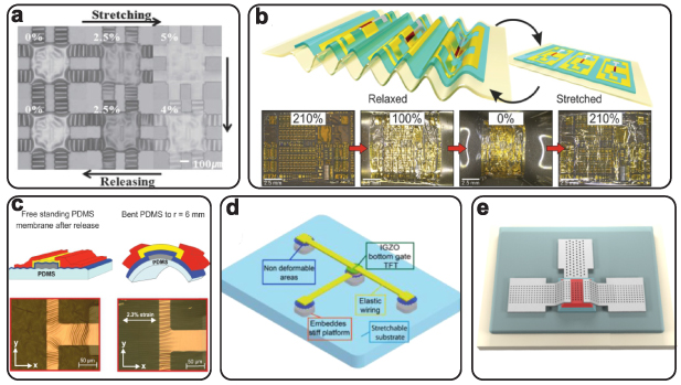
Figure 9. Microstructured substrates. (a) Wave-like bridge configuration of a transparent ZnO TFTs array [49]. (b) TFTs and circuits on 1 µm thick parylene transferred on a pre-stretched elastomer [84]. (c) TFTs directly fabricated on a wrinkled PDMS substrate [128]. (d) Long-contacts TFTs on rigid SU8 islands [134]. (e) Hole matrix patterned TFT [104]. Pictures reproduced with permission.
Download figure:
Standard image High-resolution imageMicrostructured stiff islands on the substrate aim to host no-stressed electronics when the substrate is stretched or bend [134, 137]. Figure 9(d) shows a TFT fabricated on a rigid island whose long metallic pads run towards other SU8 islands [134]. This configuration avoids any strain on the TFT when stretched up to 20%, and the flexible metallic wires ensure no fractures at the joined part. Having a good adhesion between the substrate and the island is fundamental, and a stretchable buffer stage between them can avoid the issue [137].
Moving to the design strategies, it was shown that commercial porous PET membranes (porous diameter equals 11 µm) as a substrate for Au electrodes ensured 33% higher metal conductivity, avoided Au fractures under bending compared to non-porous substrates, because of reduced tension on the PET membrane [117].
Researchers also showed that micro-patterning and the shape of the electronics materials can be adjusted to develop mechanically-resistant devices with stable or enhanced electrical parameters. As shown in figure 9(e), TFTs patterned with a matrix of holes prevented cracks propagation and device failure [104]. Semi-circular patterned OTFTs metals contacts maintained the switching behaviour under 10% of uniaxial strain while loosing of the performance was observed for a linear pattern [93]. Micro-patterned hydrogel through UV photolithography between two ITO electrodes in a capacitive pressure sensor favoured the accumulation of ions under pressure due to an increase in the contact area at the interface by improving the sensitivity [116].
4.6. Composite substrates
Composite substrates consist of a homogeneous mixture [46, 87, 279] or a heterogeneous integration [131, 135, 136, 150, 239] of two or more materials forming a substrate. Composite mixtures can enhance or reduce the properties of certain materials. For instance, a homogeneous composite ecoflex/hydrogel substrate leads to a Young modulus of 0.005 Pa that is lower than that one of ecoflex (0.69 Pa) [46]. As consequence, a metal conductor on the homogeneous composite can be stretched by 1780% without delamination while a smaller maximum strain is achieved with pure ecoflex. On the other hand, glass fabric embedded within a gel-resin favoured the reduction of its thermal expansion coefficient making it suitable for high temperature process electronics fabrication [239]. Homogeneous mixing or heterogeneous integration also allows the functionalization of the substrate. Magnetic actuation was achieved by composite shape memory substrates containing magnetic nanoparticles in a mixture [279] or dispersion [150] within the polymeric matrix. Enhanced adhesive and mechanical properties of PVA was obtained by hydrophobic-hydrophilic behaviour of UV sensitive TiO2-carbon dots (CDs) solution-processed in PVA [87].
Heterogeneous composite substrates overcome issues related to the fracture limits of electronics. Strain engineered substrates were achieved by stiff polyimide islands coated with a PDMS mixed with a photo-inhibitor solution as shown in figure 10(a) [136]. UV exposure of the PDMS softened the elastomer in the region without the island resulting in a harder area where the OTFTs were fabricated. The stiffness gradient ensured  1% of stress on the electronics when the substrate strain was up to 13%, and the fabrication can be performed without swelling of the PDMS. 0% of strain in In2O3 TFT was obtained by fabricating electronics on rigid SU8 islands patterned and embedded in a PDMS substrate [131]. Due to the stretchable composite interconnections AgNWs/Au the electronics can be contacted in a fully foldable configuration, as shown in figure 10(b). Measurements of the conductivity showed good stability of the electrical interconnection when the percolation pathway of AgNWs is coated with a Au film in a composite stacked layers PDMS/AgNWs/Au due to the embedding of the nanowires in the PDMS, while the conductivity is lost in the case PDMS/Au/AgNWs due to the mismatch between PDMS and Au causing metal cracks. To overcome issues related to interfacial stress, locally reinforce composites are proposed. Figure 10(c) depicts the distribution of iron-coated alumina plateletes in a micro-width area (down to 20 µm) within the polymeric substrate to increase the Young modulus of the substrate in that area [135]. The platelets distribution was controlled through a magnetic tape and resulted in a PDMS, PU, and PVA stiffness increase by 558%, 478%, and 265% respectively. Despite that, this strategy led to rough substrates causing an yield of 11% yield of in the TFT fabrication.

Figure 10. Composite substrate showing stiffness gradient. (a) A pentancene TFT is fabricated on a PDMS substrate coating polyimide island. The area without the islands are UV-exposed to be softer [136]. (b) Stiff SU8 islands on a stretchable PDMS enable full foldability of the substrate. The stretchable interconnections preserve the TFT functionality during different folding process [131]. (c) Schematic picture of a reinforced polymeric substrate through iron-coated alumina plateletes [135]. Pictures reproduced with permission.
Download figure:
Standard image High-resolution imageFor the sake of completeness, it is reported that also electronic materials can become composite when mixed with elastomer to achieve stretchable semiconductors [76, 230] or percolation pathways within rubbery polymers [91].
4.7. 3D substrates
Creating conformable 2D electronics on rough or not-flat surfaces remains challenging due to the rupture limits of electronics and substrates. Complex 3D substrates can be realized through 3D printing [259, 329] (section 3.4), however, there are no reports of electronics benefit from 3D printed substrate. This is mostly due to the high temperatures required for the fabrication of thin-film electronics and the chemical processes which are incompatible with materials used for 3D printing [176, 255, 262, 268]. Therefore, 3D self-assembling structures [132, 234, 240, 251, 277, 279, 280, 330–333], kirigami inspired systems [334–338], and molded substrates [133, 275] represent an alternative approach to obtain electronics-integrated into 3D architectures.
3D self-assembly processes consist of a substrate that is forming from a planar configuration, suitable for electronics fabrication, to a 3D shape. Depending on the mechanism inducing the shape morphing, micro-tubular devices [234, 240, 251, 277, 330–332, 339] and origami systems [279, 280] are distinguished. The most widely known mechanism to realize rolled-up microtubes consists in -plane stress generated between single layers of a multi-layered system. As shown in figure 11(a), the selective etching of AlAs induced the rolling of the successive layers due to built-in strain in the InGaAs/GaAs semiconducting layers [240]. Field-effect transistors were fabricated starting from the pre-strained semiconductors and the electronics performance remained stable after self-rolling. The same approach was used for a micro-battery shownin figure 11(b) [330]. Swelling processes of a hydrogel layer due to water absorption can also induce the rolling process [234, 339]. Micro-tubes were also obtained by the stress-inducing from the difference in thermal expansion coefficients of the deposited materials [277, 331]. Another way to induce rolling from a planar state is through magnetic fields. A rotating magnetic field was applied to a 2D planar nanomembrane having a magnetic film incorporated into it [332]. This resulted in a magnetic torque that assembled the structure forming a high-performance energy storage capacitor with volumetric capacity  104 C m−3.
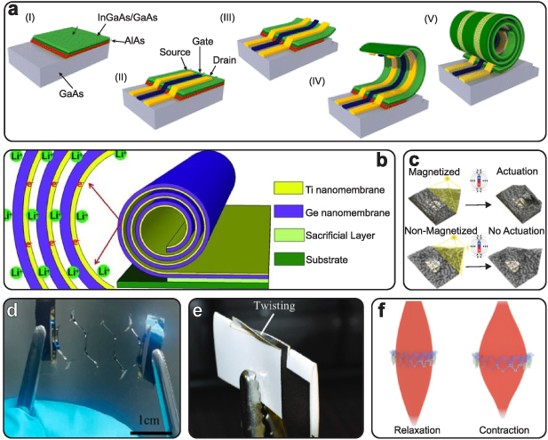
Figure 11. 3D self-assembled substrates. (a) Schematic fabrication steps of a rolled-up field effect transistor [240]. (b) Schematic picture of the rolled-up battery due to built-in strain between the Ge and Ti nanomembranes [330]. (c) Actuation behavior of the origami in magnetized (top) and nonmagnetized (down) states [279]. (d) Kirigami substrate with paper-based perovskite solar cells stretched to 150% [335]. (e) Nanosilver electrodes with a fully folded kirigami structure [336]. (f) Illustration of the kirigami-structured bioprobe surrounding the muscle [337]. Pictures reproduced with permission.
Download figure:
Standard image High-resolution imageOrigami is a folding technique that has been applied in many science and engineering fields [258]. It is beneficial in designing 3D substrates that are folded from an initial plane 2D structure. [279, 280]. An origami shape memory polymer-based structure embedded with magnetic particles was capable of assuming a 3D configuration depending on the incidence of light and magnetic field [279]. To enable the 3D substrate folding mechanism, only specific parts of the substrate were magnetized so that the planar structure could fold in specific regions (figure 11(c)). Similarly, the integration of PDMS with magnetic nanoparticles was also successful in achieving complex movements [280].
Kirigami is another technique that allows the construction of 3D structures out of planar structures [258]. Different from origami, kirigami involves cutting to resemble a 3D shape when stretched. To overcome the decrease in performance after deformation in solar cells, paper-based perovskite solar cells were fabricated with a kirigami geometry on ultrathin cellophane substrates to yield high stretchability [335], as shown in figure 11(d). This achieved a strain up to 200%, a twisting angle of 450∘, a bending radius down to 0.5 mm, and a high mechanical endurance with stable performance after 10 000 stretching, twisting, and bending cycles. Kirigami was also exploited in paper electronics (PE), to reduce the fracture of conductive nanosilver electrodes while strain was applied [336] (figure 11(e)). When compared to a similar PE in which no kirigami design was employed, these electrodes exhibited 85% lower variation in resistance during folding tests and superior durability after 100 twisting cycles. To acquire electromyography (EMG) signals and reduce the adhesion problem between muscle tissue and elastomer-based bioprobes, a donut-shaped parylene 3D substrate kirigami [337] presented better performance when compared to the traditional bioprobes (figure 11(f)). In this case, the kirigami substrate surrounded the whole muscle, resulting in a low effective Young's modulus more compatible with the muscle, a maximum stretchability around 226%, an easy fixation to the tissue, and a more stable EMG signal. Moreover, no plastic deformation was observed after 1000 loading cycles with a maximum strain around 200%.
Finally, several studies [133, 275, 340–344] presented approaches to fabricate 3D-shaped substrates pillar structures, as this allows augmented flexibility due to the reduction of the mechanical strain experienced by the electronics fabricated onto them. Here, a simple technique to achieve this is molding, described in section 3.5. For instance, GaAs solar cells were added to strain relief structures on a 3D PDMS substrate [275], providing a stretchability of 0.4% on the pillars, and an overall stretchability of 20%. Similarly, a 3D PDMS substrate composed of a 2D plane layer with bonded pillar-like structures could provide stretchability, twistability up to 180∘, and bending radii down to 6 mm [133]. Because the deformation was concentrated on the plane 2D layer, the electronics performance was not affected, by the deformation.
5. Applications
The substrate properties, the broad range of materials for thin-film electronics, and the evolution of fabrication methods allow applications in different fields. In section 5.1, biomedical systems as epidermal patches and functionalized implants are described with a special focus on edible electronics. Monitoring systems and sensors for smart agriculture and food quality control are shown in section 5.2. Section 5.3 discusses the advancements in robotics, from large to micro-scale range. The class of metamaterials and their applications in the terahertz frequency range is introduced in section 5.4. Finally, wearable systems and the integration of electronics with textiles are presented in section 5.5.
5.1. Biomedical
Thin-film electronics for health care monitoring and medical therapy have been proved. The fabrication on biocompatible active substrates and the research on bioresorbable and ingestible electronics materials, as reported in sections 2.1 and 2.2, have enabled the possibility of electronics integration on-skin as well as in-body. In the following, epidermal compliant active systems are presented and bio-implantable and digestible systems are discussed as an alternative to conventional medicine.
5.1.1. Epidermal system and artificial skin.
The suitability of thin-film electronics for on-skin applications relies on the intrinsic properties of active substrates. The employment of stretchable and flexible materials has allowed systems with proper adhesion and conformability to the epidermal roughness [46, 51, 84, 88, 91, 98, 126, 345]. Transparency and lightweight guarantee imperceptible and unobtrusive systems [51, 53, 82, 126, 141]. Hypoallergenic patches avoiding skin inflammations benefit from biocompatible materials ensuring safe electronics operations [30, 77, 88]. Additionally, they can biodegrade, allowing the development of disposable medical systems. The applications can consist on diagnostic systems [98, 126, 346, 347], wound healing process [348] or skin conditioning sensors [46, 91].
A multi-functional device for biosignal monitoring consisting of temperature, UV, electrocardiogram (ECG) sensors, and printed accelerometers, for motion sensing, was fabricated on PET and PI substrates [98]. A kirigami-like design of the substrate, as described in section 4.7, was employed to prevent stress and failure of the electronics under strain when applied on a human chest and tested during different motoric activities. The temperature and UV sensing process relied on CNT TFTs, showing a constant outcome when no temperature and light variations occurred while running/rest tests proved the ECG sensor and the accelerometer's detection capability. An EMG sensor was also fabricated on a PVA substrate because of its capability to ensure a proper adhesion on-skin [126]. Thermal treatment of PVA allowed the customization of its swelling rate due to water or moisture adsorption as described in section 2.1.3, ensuring mechanical conformability and sensor functionality. The employment of elastomers prevents electronics failures, even while a mechanical strain is applied. In this regards, organic TFTs pressure and strain sensors were fabricated by dispersing conductive and semiconducting materials within a stretchable PDMS matrix and tested as an artificial skin on a robotic hand [91]. The system was used for sign language interpretation and was characterized by a stable gauge factor around 33, while a strain from 10% to 50% was applied. A printed pressure sensor embedded on an ecoflex-hydrogel bilayer was also proposed to guarantee the electronics functionality under mechanical stress [46]. The low modulus of elasticity of the hybrid substrate, which is around 0.005 Pa, ensured a proper sensor response when applying on fingers undergoing folding/flatten cycles.
Smart epidermal systems also required the development of a wireless powering system and signal processing to be non-invasive. A Bluetooth transmission system consisting of a flexible and biodegradable sensor was proposed [88]. Despite the device being portable, it resulted in a tethered system because of the connection with the rigid electronics board. The suitability of a thin-film rectifier as wireless energy transmission circuits based on inductive coupling was proved on both parylene [84] and PDMS [51]. Although the electronics miniaturization ensured the imperceptibility of the circuit, this limits the maximum output power.
Current challenges remain the integration on epidermal patches of an efficiency powering system and the energy transmission over long distances.
5.1.2. Functionalized implants.
Researches on biocompatible materials have encouraged the fabrication of in-body devices as a promising approach for non-invasive medical procedures [60, 80, 181, 182, 184, 349] and biosignals mapping [54, 115, 132, 183, 223, 251, 350].
Materials for functionalized implants must be chemically stable when immersed in biofluids ensuring reliable electronics performance and providing sufficient mechanical adhesion on the target organ without compression damages. In this regard, shape-memory materials (section 2.1.2) have been shown their suitability because of the possibility to control their stiffness. For example, thiol-ene/acrylate is characterized by a reduction of the glass transition temperature (from 70 ∘C to 37 ∘C) when exposed to a physiological environment that lessens its Young's modulus [118]. Hence, the softening of the polymer after the implantation has been explored to develop cortical probes for in-vivo recording of the neural activity [350]. A flexible polyimide/PDMS substrate that can be wrapped around blood vessels by air-pressure control, as described in figure 6, has also been proposed to achieve proper implant adherence [132]. Here, thin-film temperature and strain sensors were fabricated showing a reliable detection of blood vessels pulses compared with the conventional measuring system.
Vital signals monitoring also demand a data acquisition and transmission system. In-vitro experiments on a Swiss-roll nerve cuff (described in section 4.7) have reported the performance of IGZO transistors and circuits in detecting ionic liquid when neural stem cells were growth within the micro-tubular structure [234]. It was also proved the monitoring of cardiac cells proliferation in a tissue-repairing patch due to interaction between the cells in a nanofibre scaffold coating a Au electrodes matrix [349]. Here, the electrodes were used for signals detection from the cells and their stimulation, but also to activate the release of drugs hosted in a porous hydrogel membrane within the matrix, as shown in figure 12(a). The charged structure of the hydrogel allowed the on-demand release of the drug molecules stored in the hydrogel matrix thanks to its swelling during immersion in the solution. To achieve a transmission system in in-vivo and untethered system, as well as the control of the implants functionalities, electronics, and biological parameters, have been accounted for a trade-off between antenna dimensions and power efficiency. As an example, a miniaturized helical antenna was optimized to provide good efficiency in industry-scientific frequency and accounted for signal penetration between human tissue [251].

Figure 12. Schematics of functionalized implants. (a) Cardiac patch consisting of electrodes for signals detection and stimulation, a nanofiber scaffold for cardiac cells growth, and an electroactive polymer for drug encapsulation [349]. (b), (c) Wireless bioresorbable electronic systems for neuroregenerative. Both the implants consist of a receiver antenna, and Si-based diode and capacitor are RF powered. In (b), Mg wires connect the antenna to the PLGA cuff for nerve stimulation. [60]. In (c), Mo wires in a serpentine-design connect the antenna to the PLGA cuff for nerve stimulation. The polyurethane based encapsulation (b-DCPU) enhances the device stretchability [181]. Pictures reproduced with permission.
Download figure:
Standard image High-resolution imageTransient materials for implantable systems have gained attention for the possibility to preserve stable functionality before dissolution in the surrounding environment, leaving no harmful residuals [54, 55, 60, 115, 181–184]. Despite surgical processes are still required for the implantation, the implanted devices can overcome the limitations of standard therapies enhancing the effect of the treatment, and their bioresorbability prevents possible injuries from a second extraction surgery [60]. Here, a wireless receiver antenna (figure 12(b)) interconnected with a Mg electrode-cuff was encapsulated in a 30 µm thick PLGA substrate and used for in-vivo electrical stimulation of nerve and muscle. The device resulted in a quicker recovery when compared to standard therapies, and the resorption of the system within 2 months was ensured by both the PLGA dissolution and electronics encapsulation. Due to the dependence of the transient time on the PLGA thickness, it is possible to customize the device's working time [54]. Here, a multiplexed array of Si NMs metal oxide semiconductor field effect transistor (MOSFET) (from 64 to 128) was also fabricated on the same substrate for recording cerebral cortex activity. In-vitro experiments demonstrated the dependence of dissolution time on doping and thickness of the NMs allowing a proper design of the system according to signal monitoring duration. The performance of the device was validated by comparison with clinical equipment and carried out over one month, suggesting the importance of wireless data communication system. A wireless and bioresorbable heating system based was also fabricated on silk natural fiber [182] because of its proved biocompatibility [55]. Additionally, wireless data circuits must be conformable to guarantee the signal acquisition over prolonged periods. As it is shown in figure 12(c), an elastic and bioresorbale polyurethane encapsulation combined with serpentine Mo electrodes allowed the minimization of mechanical stress on the electronics during in-vivo tests that could cause device failure [181]. This design, as described in section 4.5, reduced the electronics strain and ensured a stable operation up to a maximum uniaxial strain of 20% and a dissolution time of 50 d.
The rapid advances in materials and system functionality have guided the exploration of digestible and edible electronics [36]. This new class of smart implants envisions the tracking of biomedical signs and disorders by inserting electronic systems in the gastrointestinal tract, paving an innovative route in the field of health monitoring and telemedicine. Although initial prototypes were suitable only for swallowing (endoscopy capsules [351] and smart pills [352, 353]), the ongoing trend in this field is to design and realize completely digestible systems, safe for both the human body and the environment, with no need of recollection [36, 352]. Fully functional systems require the combination of sensing or actuation features (i.e. temperature, pH, gas, pump reservoir), with powering (i.e. batteries) and data transmission unit (i.e. antennas), reducing the risk of rejection [354]. To achieve these requirements, a step forward is constituted by the use of biocompatible, transient, and natural food-based materials in the device stack [355]. Passive components, such as capacitors, antennas, conductors [356], as well as active devices, like field-effect or electrolyte-gated transistors [81, 140, 357, 358], filters [359], and logic circuits [358], have been presented.
5.2. Smart agriculture and food monitoring
Besides medical applications, the biocompatible, and transient properties of certain types of electronics have also applications in the production, storage, and distribution of food. Although the deployment for soil and food monitoring is still at early stage, key properties of smart and active systems, including mechanical flexibility, real-time sensing, and actuation, will certainly open up future opportunities. In particular, the following two application scenarios promise to become more and more important in the near future: (a) mapping of the fruit ripening processes [360, 361], monitoring of the environmental conditions [43], as well as the presence of nutrients, toxicants and pest infestations in the field. This enables the efficient and localized use of fertilizers, insecticides, herbicides, and fungicides, for a smart approach to agriculture inspired by Industry 4.0 [362]. The required systems have to be cheap, compatible, environmetally-friendly and operate without an external power supply. Ideally, they will dissolve after fulfilling their respective task, without leaving behind any harmful substances [363]. (b) Monitoring of food quality. On one hand, this can concern environmental parameters in particular during the transport and retail phase and can e.g. help to guarantee sufficient cooling of perishable goods [364]. On the other hand, this involves the reliable analysis and detection of residuals and foodborne toxicants [365]. Finally, chemical sensors inside the food packaging can detect indicators of food spoilage [366] or ripening, such as gas production (ethylene [367]), humidity and temperature variations, as well as bacteria growth [368, 369]. In this way, the whole supply chain and logistics will be monitored, and customers will be safely guided, reducing the risk of food poisonings.
5.3. Robotics
From the macro- to the microscale, artificial robotic systems have supported and influenced our daily-life for decades. A natural evolution for them to further expand their applications fields relies on the integration with materials and electronics for sensing, data transfer, and remote control. Here, robotic systems are presented. For the sake of comprehensiveness, in section 5.3.1, an overview on how substrates and thin-film electronics are integrated with sensing elements and actuators as a part of soft and macroscale ( cm2 scale) robots, is reported. In section 5.3.2, the attention is focused on the achievements and current issues in the development of autonomous microscale (
 mm2 scale) machines and smart micro-systems.
5.3.1. Soft robots.
Soft robots have been gaining attention in the last few years for being composed of flexible components that exhibit many capabilities, including high stretchability, the ability to conform to irregular geometries or surroundings and interact smoothly with biological tissues [262, 370–373].
Substrates can be used as components of sensors or actuators in soft robots. For sensing applications, they are integrated on the soft robot's external surface for proprioception, temperature, tactile, or force sensing [50, 374]. For actuating, they can be used to hold and guide the moving components [99] or they can be the actuators themselves (section 6).
Electrically conductive silicone filled with carbon black was used to realize kirigami-inspired soft strain sensors, enabling a feedback of the 3D configuration of the structure [375] (figure 13(a)). To measure objects slippage, PEN was used to fabricate a ferroelectric polymer-based soft sensor considering parallel and perpendicular forces (figure 13(b)) [121]. A PDMS layer was employed to form a substrate for a T-type and a K-type thermocouples that were integrated on a soft micro-finger, conferring tactile sensing abilities to the soft robot [376]. Figure 13(c) shows a close-up view of the T-type temperature sensor. Additionally, some applications can utilize substrates inside the robot structure rather than on the external surface, as demonstrated by Xie et al [100]. Here, a flexible piezoelectric PVDF thin film combined with jamming layers was developed to provide proprioceptive sensing (figures 13(d) and (e)).

Figure 13. Active substrates in soft macroscale ( cm2) robots. (a) Pneumatic soft robot with a kirigami-shaped sensor on its surface for proprioception sensing [375]. (b) Sensor for Object slippage [121]. (c) T-type thermocouple for a soft microfinger [376]. (d) Soft robot finger with multifunctional jamming/sensing structures [100]. (e) Three fingers gripper for grasping [100]. (f) Beginning (left) and end (right) of a rolling movement to mimic inchworms locomotion [48]. (g) Beginning (left) and end (right) of the actuation movement of an electrically driven flower-shaped [130]. Pictures reproduced with permission.
Download figure:
Standard image High-resolution imageAs part of actuators, PDMS was combined with PI and Au to realize a bio-inspired ultra-thin controllable device that could simulate the movements of a chameleon's tongue to hunt moving insects or mimic the plant's vine in winding around a tiny pole [110]. A combination of Au electric traces in a liquid crystal elastomer doped with carbon black (LCE-CB) with a PI substrate layer was used to selectively control different parts of the substrate (figure 13(f)), mimicking the locomotion patterns of inchworms [48]. In another example, the shape morphing was controlled through a combination of PDMS with PEDOT:PSS with hygroscopic properties to form a single composite material that could change through specific environmental humidity or the application of electrical current [130]. Figures 13(g)–(h) show the robot in non actuated and actuated states, respectively.
5.3.2. Microrobots.
Miniaturized systems have been gained attention for the envisioned functionalities they could achieve in medical technologies [377], such as drug delivery, or non-invasive surgery, and for environment sensing and pollutants degradation in energy and green application [378]. Despite smart micro-machines, such as self-propelled micro-engines [379, 380], cargo loading/transport platform [381, 382], and locomotive programmable and controllable micro-system [383, 384] have been realized thanks to the materials and technologies innovations, the micro-scale geometry has limited the electronics integration. These limitations are mainly represented by temperature and chemicals sensitivity of the employed materials (such as elastomers and hydrogels) as well as their flexibility leading to substrate swelling [128, 131]. A possible way to overcome these limitations is the employment of standard rigid electronics carried on a silicon wafer that does not undergo mechanical deformation during the electronics fabrication allowing for dimensions scaling. An example of silicon electronics-based walking micro-robots with 7 nm thick Pt based electrochemical actuated legs were reported [222]. Standard electronics fabrication followed by a PDMS stamp transfer process (section 3.6) ensured a large area fabrication of floating microrobots, as shown in figures 14(a) and (b). The electronics actuation by laser powering ensured the travelling speed of the microrobot of 1 µm s−1, as described in section 4.1, offering a strategy for micro- and nano- objects manipulation (figure 14(c)). Nevertheless, the micro-systems bodies consist of 5 µm thick rigid electronics, far from lying to thin-film electronics definition.
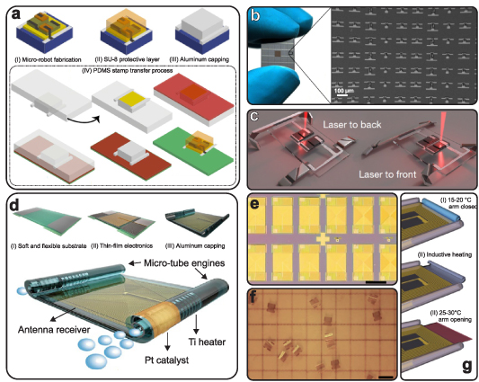
Figure 14. Untethered microscale ( mm2) robots. (a)–(c) Electronically integrated micro-machine. (a) Fabrication process: after silicon electronics fabrication and integration of the soft-legs actuators, a SU-8 protective layer capped with Al prepare the electronics to the silicon etching. Floating microrobots are obtained by PDMS stamp assisted transfer process. (b) Optical image of a silicon chip showing the large-scale fabrication. Scale bar 100 µm. (c) Conceptual image of laser powered walking micro-robots [222]. (d)–(g) Flexible micro-machine. (d) Fabrication process: thin-film electronics consisting in antenna coil, Ti heaters, and Pt catalyst are fabricated on a soft and flexible hydrogel/polyimide bilayer. Hydrogel selective etching induces the rolling and forms the micro-tube engines. (e) Microscope image of micro-robots array. (f) Microscope image of a micro-robots swarm in solution. Scale bar 1 mm. (g) Micro-arm thermally actuated [241]. Pictures reproduced with permission.
Download figure:
Standard image High-resolution imageRecently, a self-propelled flexible platform equipped with a micro-arm to grasp, transport and release micro-objects was obtained by thin-film electronics integration [241]. The micro-system was built on bilayer hydrogel/polyimide substrate to host an on-board circuit consisting of Au receiver coil and two Ti heaters in contact with Pt electrodes. Using a transfer process (section 3.6), the electronics fabrication was carried out on a rigid carrier and then released for experimental studies, where the flexibility of polyimide ensured mechanical stability to the whole system. Repeated compressive tests of the whole micro-system were performed showing the full shape recovery after each cycle. The rolled micro-engines at the edges of the system were obtained by hydrogel swelling during sacrificial layer dissolution, as described in section 4.7, forcing the bending of the polymeric substrate. Figure 14(d) depicts the fabrication steps and the final micro-system. With the same process, a micro-arm was obtained consisting of a hydrogel layer coated with a Fe/Au layer. The self-propulsion was achieved by catalytic reaction of the Pt micro-engines in a hydrogen peroxide solution. A wireless system was used to transfer the energy from an external coil to the receiver one through inductive coupling and employed for three purposes. First, it was used to heat the Pt engines through the heater allowed the locomotion control in terms of speed and directions. Next, the Fe/Au micro-arm was heated to induce rolling/relaxing (grasping/releasing) of the temperature responsive hydrogel, as shown in figure 14(g), and the transport of a Au wire was proved. Finally, the wireless energy transfer was proved by switching an integrated IR-LED showing an efficiency of 37% of the transmission/receiver energy system. The micro-robot provided a valid example of a smart and multifunctional micro-system. Although that, the use of a non-biocompatible fuel, such as H2O2, as well as the electronics energy demand and supply must be accounted for applications in the microscale range and, potentially, in-vivo.
5.4. Terahertz metamaterials
Terahertz metamaterials have been used as polarizers [309, 312, 313, 318, 322], anti-reflexive layers [316], modulators [323, 385] and absorbers [324]. They primarily relies on polymeric [242, 309, 312, 313, 316, 318, 321, 322] or rigid [237, 242, 323, 324] substrates that interacts with patterned metal layers, enabling the manipulation of the terahertz frequencies.
Modulation is also possible through active electronics. For example, a monolithic terahertz metamaterial structure composed of quartz as the substrate and an array of a-IGZO TFT as the unit cells was developed to manipulate terahertz frequencies [237]. The absorption depth was modulated by tuning the a-IGZO conductivity via external electrical bias, which can be a promising tool for efficient real-time control and manipulation of frequencies. A conductive range up to 40 S m−1 with a resonance at 0.75 THz and a 4 dB relative intensity change at a forward gate bias of 24 V was verified. Figure 15(a) shows the incident terahertz waves being modulated by the array of TFT and figure 15(b) presents a zoom of the structure, showing the layers of the a-IGZO-TFT.

Figure 15. Teraterhz metamaterial device. (a) Schematic illustrating the contacts (source, drain, and gate) of the IGZO-TFT array [237]. (b) Close-up view of the structure with each transistor layer [237]. Pictures reproduced with permission.
Download figure:
Standard image High-resolution image5.5. Electronic textiles
Flexible electronics combined with textile structures were employed for numerous wearable and smart textile applications [386]. Textiles are comfortable to wear and can conform onto human body shapes due to the textile's ability to bend, drape and sheer. In general, electronic components are bulky and rigid making them less desirable for smart textile applications. The flexible nature of thin-film electronics makes them a preferred alternative for smart textiles. Some researchers have developed thin-film devices for smart textiles utilising textile fibres and textile structures as substrates [96, 111, 142, 196–203, 205–214, 227, 387, 388]. These devices were fabricated by either employing vacuum-based thin-film technologies (section 3.1) [113, 196, 199, 200], solution-based processing (section 3.2) [201–203, 207, 209, 210, 212, 213], molding (section 3.5) [198] or cilia assisted transfer printing (section 3.6) [62]. Subsequently, others have textiles carrying prefabricated thin-film devices within it [47, 62, 92, 95, 97, 113, 119, 146, 204, 215, 217–219, 227, 389, 390].
5.5.1. Textiles comprising of thin-film conductors and sensors.
A preeminent factor when fabricating electronic textiles is to identify methods of creating conductive pathways and structures in the textile. To this end, researchers have investigated the feasibility of creating simple thin-film structures such as electrodes and resistors [62, 199–201, 212, 214]. These devices were either fabricated directly on a textile substrate (an example of this is displayed in figure 16(a) [199–201, 212], created using a textile manufacturing technique [214], or transferred onto a textile structure as shown in figure 16(b) [62].

Figure 16. Smart textile carrying flexible electronics. (a) A resistor created on a cordura composite substrate using laser treatment on a silver layer [200]. (b) Cilia-assisted transfer printing of ultrathin devices onto a textile [62]. (c) 3D sketch of a temperature sensor fabricated on a yarn substrate [113]. (d) Light emitting device fabricated on a substrate comprising of polypropylene fibres [146]. (e) A schematic of the perovskite solar cell and super capacitor on a flexible PET substrate for smart textile applications [119]. (f) Circular knitted energy generator using nanostructured hybrid PVDF/BT fibers [208]. Pictures reproduced with permission.
Download figure:
Standard image High-resolution imageThe ability of textiles to comfortably drape over several areas of the human body enables sensors integrated on or in the textile to closely monitor important parameters of the body. Therefore, sensing textiles is one of the most prominent areas of research in electronic textiles [195]. Several textiles carrying thin-film sensors were fabricated, and in other cases, the textile itself was used as a substrate [92, 95, 96, 96, 111, 113, 146, 198, 207, 387]. Since temperature is one of the most commonly measured human vital signs, several thin-film temperature sensors were synthesised on textiles or integrated into textiles [95, 96, 111, 113, 207]. Woven polyimide temperature sensor strips with a tolerance of 2.5% were fabricated by utilising platinum as a sensing layer [95]. The bendability of polyimide substrates ensures the high flexibility of the smart textiles in a single dimension. Subsequently, Au thin films were also utilised as sensing layers on the same substrates to fabricate temperature sensors with a temperature coefficient of resistance of  ∘C−1 [96]. Similar devices to the aforementioned once were incorporated within textile yarns [111]. The temperature coefficient of resistance of the different sensing yarns varied from
  ∘C−1 to
  ∘C−1. Moreover, researchers have built temperature sensors directly on nylon yarns by depositing Au, and utilising planar and tube masks [113]. A schematic of a patterned yarn is illustrated in figure 16(c). These sensors had a temperature coefficient of resistance of
  ∘C−1. Textile yarns and fibers are the raw materials for creating textile fabrics, therefore, developing devices on yarns ensure smooth integration of these devices within a smart textile. A yarn-based temperature sensor with a sensitivity of
  ∘C−1 (range of 30 ∘C–65 ∘C) was fabricated by coating a PET fibre wrapped in a silk yarn with a mixture of carbon nanotubes and an ionic liquid (
![$[EMIM]Tf_2N$](https://content.cld.iop.org/journals/0022-3727/55/32/323002/revision2/dac6af4ieqn42.gif) ) [207]. This yarn was used to fabricate a textile glove capable of monitoring temperature.
) [207]. This yarn was used to fabricate a textile glove capable of monitoring temperature.
Textile structures are able to compress, deform, and in some cases stretch to maintain their drape during bodily movements. These features are utilised to fabricate strain, tactile, and pressure sensors for wearable applications [96, 198, 207, 213, 387, 389, 390]. Woven strain gauge strips able to respond to strains from 5% to 9% were created by utilising a Au conductive layer and a polyimide substrate [96]. A different strain sensor, created by sandwiching PET fibers in between polyethylene films and then depositing conductive fillers comprising of PEDOT:PSS and silicone, demonstrated a gauge factor of 6.9 for strains up to 5% [198]. Pressure sensors able to showcase a maximum gauge factor of 10 (for compressive strain from 2% to 10%) were created by utilising a 3D printed sacrificial mold (moulding is explained in section 3.5) to surface-embed a graphene coating on a porous silicon substrate [390]. A wristband carrying the sensor was able to detect the pulse of a person having a heartbeat rate of 68 bpm. A woven capacitive pressure sensor built using two crossing silk fiber-wrapped polyurethane (PU) yarns coated with silver nanowires as electrodes and ecoflex as a dielectric insulating layer had a sensitivity of 0.136 kPa−1and a relaxation time of 0.25 s [207]. A machine-washable pressure sensor, fabricated by sandwiching a PET microfiber textile layered with PEDOT in between two nickel-plated fabrics, had a response and recovery time of 52 ms and 22 ms respectively [387]. This device was able to withstand 2000 cycles of folding and the resistance of the device changed from 20 Ω to 15 kΩ when the pressure was changed from 39 kPa to 33 Pa. A capacitive/resistive touch display having a rise and fall time of 1.4 ms was fabricated by the transfer of CVD graphene onto a tape-shaped polypropylene fibre [146]. In the same work a LED display (shown in figure 16(d)) with an emission peak of 500 nm was synthesised by spin coating ZnS:Cu and BaTiO3 onto polypropylene fibres [146]. The device was able to withstand a bending radius of 10 mm and repeated torsion ( 1000 cycles). Nevertheless, these polypropylene tapes are incapable of sheering and drape which makes them less desirable for smart textile applications.
The fact that people are comfortable wearing textiles on their bodies makes it desirable to have more distinct sensors such as electronic noses within the textile structure. A textile carrying electronic nose strips were able to detect acetone (down to 50 ppm), toluene, IPA, and methanol [92]. These devices were fabricated on PEN and kapton subtrates, and they were woven into a textile. PEN substrate shows mechanical limitations similar to polyimide, where they are also unable to sheer or drape around a surface. Four different sensors were fabricated utilising non-conductive polymers (poly-iso-butylene PIB, poly-styrene PS, poly(N-vinyl-pyrrolidone) PVP and, poly-vinyl-butyral PVBU) mixed with carbon black as the conductive filler.
5.5.2. Thin-film technologies to power electronic textiles.
Smart textiles with energy sources can provide power to wearable devices [391]. Thus researchers have developed electronic textile with solar cells [119, 197] and generators that utilise piezoelectricity [208, 209], triboelectricity [47], pyroelectricity [388] and thermoelectricity [211]. Textiles carrying thin-film solar cells that convert energy of light directly into electricity were utilised for power generation applications [119, 197]. Two differently configured solar cells were fabricated using amorphous silicon and interwoven metal wires [197]. In one, glass fiber fabrics were utilised on top of the device; whereas, in the other configuration, glass fibers were utilised as the substrate. The device that was built with the glass fibres as substrate demonstrated superior performance showcasing a open-circuit voltage of 0.88 V, short-circuit current density of 3.70 mA cm−2, fill factor of 43.1%, and an efficiency of 1.41%. Furthermore, a thin-film perovskite solar cell and supercapacitor woven into a textile had a short-circuit current density of 16.44 mA cm−2, open-circuit voltage of 0.96 V, fill factor of 0.66, and a power conversion efficiency of 10.41% [119]. Although, the device had multiple layers comprising of PEDOT:PSS/methylammonium lead iodide(perovskite layer)/phenyl-C61-butyric acid methyl ester/Cu(OH)2 nanotube/copper ribbon, the fabrication on a ITO/PET substrate, limits the conformability of the device around a curved surface
Textile structures are able to withstand mechanical stresses such as compression and bending. Hence, they are well suited to utilise the piezoelectric effect in order to produce electrical energy [208, 209]. Piezoelectric generators were created on woven textiles by screen printing layers constituting of a lead zirconate titanate (PZT) and silver nano particles as the piezoelectric film [209]. This film was sandwiched between two silver polymer ink electrodes. Three woven substrates polyester-cotton, cotton and polyamide-imide (Kermel) were tested. The maximum energy density under an 800 N compressive force was showcased by the Kermel textile at 34 J m−3, whereas cotton textile demonstrated the maximum energy density under bending at 14.3 J m−3. A piezoelectric yarn was fabricated utilising a three layer structure comprising of a silver-coated nylon core electrode, a circular knitted barium titanate nanoparticle and poly(vinylidene fluoride) (PVDF) nanocomposite fibers layer and a braided silver-coated nylon outer layer [208]. This yarn structure is displayed in figure 16(f). The yarn generated an open-circuit voltage of 4 V and an output power density of 87 µW cm−3 during cyclic compression.
A textile's ability to conform onto the human body and move with it, ensures that it can be used as a platform to harvest energy from human motion [47, 210]. A triboelectric generator capable of converting mechanical energy to electricity was synthesized by spray coating a CNT-silk layer on an electrospun silk fiber layer [210]. The device generated a power of 317.4 µW cm−2 from hand patting (force of 20 N with a frequency of 7 Hz). Moreover, researchers have woven coaxial fiber shaped triboelectric nanogenerators to produce a current of 210 µA and a voltage of 40 V corresponding to an output power of 4 mW under a cycled compressive force of 40 N [47]. The coaxial cables were made by growing ZnO nanowires on an aluminium wire, followed by the deposition of a Au thin-film and this structure was inserted into a PDMS tube.
The close proximity of textiles to the human body enable them to harvest the heat generated by the body [211, 388]. A pyroelectric nanogenerator capable of generating a current and voltage of 2.5 µA and 42 V respectively for breath temperature changes (12 ∘C variations) was fabricated by sandwiching a PVDF film in between two aluminium films and attached to a mask [388]. Similarly, a cotton fabric substrate coated with reduced graphene oxide and PEDOT:PSS was used to create a thermoelectric nanogenerator [211]. The device showcased a Seebeck coefficient of 25.5 µV K−1 and a power factor of 0.25 µW (m K2)−1 for a temperature gradient of 16.5 ∘C.
Another crucial aspect to consider is data and power transmission for on body wearable applications. Metamaterial textiles carrying pressure sensors were able to support surface-plasmon-like modes of communication frequencies and provide a platform to propagate radio-waves around the body [389]. Metamaterials are described in paragraph 4.3. The relative signal strength indicator averaged over 32 dB for the device and it was able to transmit an output power of 20 dBm (100 mW) at a transfer efficiency of 10.5% to a loop antenna and 3.5% to a LED. This metamaterial textile improves the transmission efficiency of wireless networks by  30 dB compared to conventional radiative networks and provides secure localized measurements within 10 cm of the body.
5.5.3. Electronic textiles supporting transistors and circuits.
Textiles carrying transistors provide wearable devices and electronic textiles with the requisite functionality of modern-day electronics. For smart textiles, thin-film transistors were either prefabricated and integrated onto textiles [62, 97, 204, 215, 217–219, 227], created using textile structures and enhanced fibres [142, 202, 203, 205] or synthesised directly on textile fibres [196, 206]. In most cases researchers have textile structures carrying prefabricated transistors [62, 97, 204, 215, 217–219, 227]. Early work investigated the feasibility of weaving in amorphous silicon transistors fabricated on SiNx–coated Kapton fibers [97]. These transistors demonstrated a threshold voltage of 7.5 V and a linear electron mobility of 0.13 cm2 V−1 s−1. Moreover, a textile ribbon structure enabled the creation of transistors by gluing the gate, dielectric and semiconductor onto it [204]. Two gold wires crossing the device acted as the source and drain. The proposed transistor exhibited limited performance and only produced a drain current of around −10 nA for gate voltages of −80 V. A complex 7-Stage ring oscillator was developed on a textile as shown in figure 17(a), by using cilia-assisted transfer printing of IGZO transistors [62]. The transistor was created on a polyimide substrate utilising SiO2 as a buffer layer and dielectric, Mo as the gate dielectric, Au/Cr layers as the source and drain electrodes and a passivation layer of SU8. The transistor demonstrated an  current ratio of 108. In the case of the ring oscillator at a V
 of 10 V the output voltage oscillated with a frequency of 33 kHz and a propagation delay of 2.2 µs.
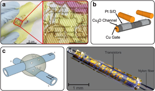
Figure 17. Different fabrication techniques of transistors on textiles. (a) An IGZO-based 7-stage ring oscillator transfered onto a textile hanker chief utilising cilia assisted transfer printing [62]. (b) A transistor schematic of a Cu wire substrate having an outer shell of Cu2O and Pt pads for the drain and source [215]. (c) Schematic picture of a transistor synthesised by adding a drop of polymer electrolyte at the junction of two PEDOT/PSS coated fibres [202]. (d) Micrograph of a transistor transferred on a nylon wire [196]. Pictures reproduced with permission.
Download figure:
Standard image High-resolution imageThe cylindrical surfaces of metal wires and optical fibers also enabled the fabrication of transistors [215, 217–219, 227]. Maccioni et al created an organic field-effect transistor by evaporating pentacene on a metal wire and created two devices one with source drain contacts made of gold and the other with PEDOT:PSS. Both the devices had an  current ratio of 103 and the transistor created with PEDOT:PSS showcased the best performance demonstrating a 0.06 cm2 V−1 s−1 while functioning at a threshold voltage of 0.6 V. Thin metal wires are well suited for smart textile applications because of their ability to undergo multi-axial bending. Indeed, heated copper wires with a copper oxide shell structure with the source drain electrodes evaporated on it as displayed in figure 17(b), was utilised to form a transistor [215]. A woven structure was used to connect perpendicular wires to the source and drain electrodes. The device had an
  current ratio of
  and a channel mobility of 26.3 cm2 V−1 s−1. However, it had a gate leakage current which made it undesirable for developing circuits. Nonetheless, the device demonstrated an 82% change in drain current when the relative humidity was varied from 0% to 70% making it a potential humidity sensor. Subsequently, transistors were also fabricated on optical fibers [217–219], although their limited flexibility makes them less desirable for most smart textile applications. These devices were fabricated by depositing chromium and AlOx
on the optical fiber for the gate electrode and dielectric respectively. Park et al dip coated it with a InOx
or IGZO precursor solution [217]. The source/drain electrodes were made by depositing aluminium and the device showcased a field-effect mobility and an
and a channel mobility of 26.3 cm2 V−1 s−1. However, it had a gate leakage current which made it undesirable for developing circuits. Nonetheless, the device demonstrated an 82% change in drain current when the relative humidity was varied from 0% to 70% making it a potential humidity sensor. Subsequently, transistors were also fabricated on optical fibers [217–219], although their limited flexibility makes them less desirable for most smart textile applications. These devices were fabricated by depositing chromium and AlOx
on the optical fiber for the gate electrode and dielectric respectively. Park et al dip coated it with a InOx
or IGZO precursor solution [217]. The source/drain electrodes were made by depositing aluminium and the device showcased a field-effect mobility and an  current ratio of 3.7 cm2 V−1 s−1 and
  respectively. In contrast, Heo et al utilised SWCNT network as the channel layer [218, 219]. Au electrodes were utilised with non-isolated and isolated SWCNT channels to achieve an
  current ratio of 105 and a field-effect mobility of 3.61 cm2 V−1 s−1 [219]. Alternatively, in another paper dry spun conductive carbon nanotube fibers were sewn in as source/drain electrodes [218]. This device had a saturation mobility of only 0.56 cm2 V−1 s−1. Nonetheless, a pressure sensor was developed using this transistor which had a sensitivity of
  Pa−1 and
  Pa−1 for pressure ranges of 0–32 Pa and 32–280 Pa respectively.
Researchers have combined multiple fibres with various textile structures to construct transistors for smart textiles [142, 202, 203, 205]. Organic transistors were fabricated by adding a drop of polymer electrolyte at the junction of two PEDOT/PSS coated fibres [202]. This structure is illustrated in figure 17(c). The coated fibres were running perpendicular to one another and a woven textile was utilised to realise the structure. The transistors had an  current ratio
  for gate voltages ranging from 0 and 1.5 V. These transistors were utilised to create an inverter and multiplexer. A similar transistor was fabricated by twisting two PEDOT:PSS coated kevlar yarns and putting a drop of electrolyte [203]. This new method of creating transistors utilising twisting ensured that the device can be integrated more easily into different textile structures rather than just woven once. In this way, an analogue amplifier with an amplification of 7.5 was created and the transistor showcased an
  current ratio of
  . A more recent publication has fabricated a transistor utilising three twisted Au microfibers [142]. Here, for the source and drain electrodes the microfibers were coated in P3HT solution, then twisted together and an ionic gel was dropped on the twisted structure. Thereafter the Au microfiber for the gate electrode was wound around ion-gel and then passivated using Ecoflex. The device showcased
  current ratio of
  at drain and gate voltages below −1.3 V. The device had a transconductance and a threshold voltage of 111.8 µs mm−1 and −1.01 V respectively, these values were maintained up to 80% after bending over a radius of 2.0 mm. Biosensors were achieved by creating a transistor comprising of a source drain synthesised of different ion selective membranes around a PEDOT:PSS soaked acrylic textile yarn substrate and a Ag/AgCl wire for the gate electrode [205]. One device had a potassium selective membrane solution and was able to detect concentrations of potassium from 10−4 mol to 1 mol with a selectivity of 20.34%. The other transistor had a calcium-selective membrane and was able to detect calcium ions in concentrations ranging from 10−4 mol to 10−1 mol with a selectivity of 12.19%. Both the transistors also responded to changes in sodium concentration.
Textile fibers can be directly employed as substrates when fabricating transistors [196, 206]. Devices engineered on nylon and glass fibers showcased limited performance with an  current ratio of
  and 104 (functioning only in depletion mode with a threshold voltage of −12.5 V) respectively [196]. In the same work devices fabricated on a silicon wafer were transferred to textile fibers utilising a parylene membrane and these transistors demonstrated an
  current ratio of 107 and a field-effect mobility of 7.2 cm2 V−1 s−1. A microscopic image of a transistor synthesised on a nylon yarn is displayed in figure 17(d). In a different work, a p-type transistor was synthesised by drop casting a semiconductor solution on a linen thread and then knotting Au wires as the source and drain contacts [206]. Two semiconductor solutions were tested CNTs and organic semiconductor P3HT (regioregular poly(3-hexylthiophene)). They both had limited
  ratios of
  and the transistor made with CNT had a linear mobility of 3.6 cm2 V−1 s−1.
6. Summary
The advancements in materials and technologies employed for electronics fabrication have enhanced the application of thin-film electronics on several fields. Figure 18 provides an outlook on the current achievements of the active substrates presented in this review.
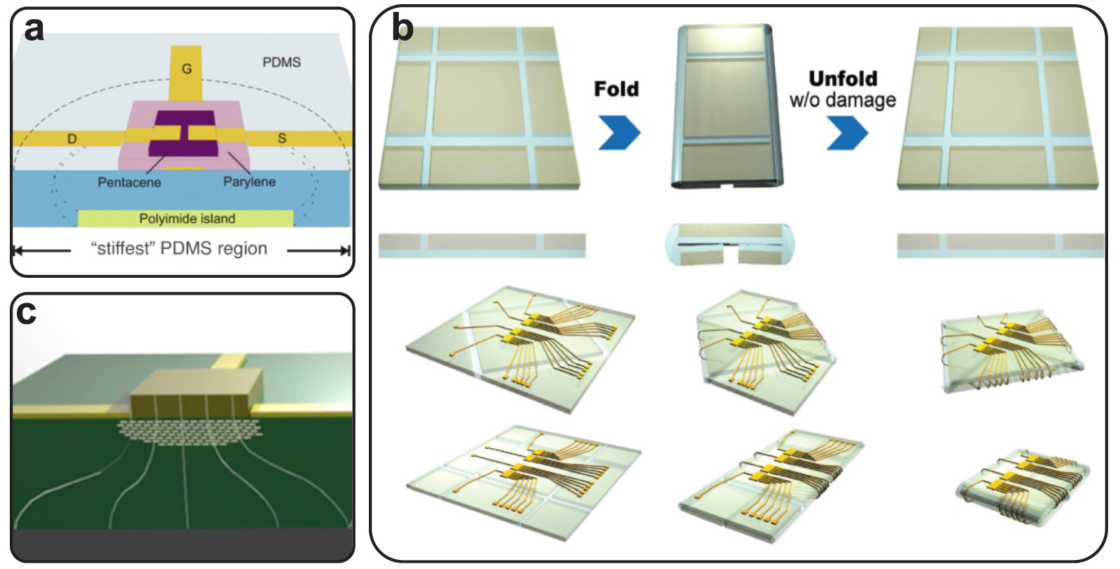
Figure 18. Outlook on the applications of active substrates for thin-film electronics as biomedical devices, soft robots, smart textile and wearables, metamaterials, as well as sensor systems [46, 47, 50, 54, 55, 60, 88, 92, 98, 113, 118, 130, 140, 142, 185, 212, 213, 237, 312, 389]. Pictures reproduced with permission.
Download figure:
Standard image High-resolution image
Polymers have been shown to be the most employed substrates because of the several classes of materials gathered in this group. The thermal and chemical instability of some polymers during electronics fabrication have been overcome by transfer printing process and micro-fabrication strategies, while composite polymers ensured the mechanical stability of the electronics under stress. Accordingly, thin-film electronics on polymers have been proved outstanding performance in applications as biomedical epidermal systems, implants, and wearable sensors integrated on textiles. Soft sensors and actuators have also been developed as part of robotic systems, while electronically integrated micro-scaled robots remain challenging.
Shape memory materials as a substrate for thin-film electronics are mostly polymer-based. They have been largely exploited in many applications such as implantable biomedical devices, soft robotic tactile and sensing systems because of their ability to reshape in a controllable way. However, there are still no reported approaches of epidermal patches and wearable devices that benefit from the integration with thin-film electronics. Shape memory polymers might not be suitable for metamaterials applications due to the loss tangent variation when triggered by temperature [392].
The programmable lifetime of electronics on transient substrates has defined the suitability of these materials as in-body implants and on-skin sensors. The absence of toxicity and inflammations issues from the in-vivo experiments, and the amount of residuals after materials dissolution lower than the accepted daily intake were reported as a proof of their biocompatibility [54, 60, 79]. Future works could be slowly go toward the implementation of real studies and tackle specific surgery, to achieve real applications in human beings..
Textiles have been used as active substrates because of their ability to withstand severe deformations which makes them highly desirable for wearable applications. For this reason techniques such as deposition [113, 196, 199, 200], coating [201–203, 207, 210, 212, 213], vapour phase polymerisation [387], moulding [198], drop casting [206], printing [209] and cilia assisted transfer printing [62], were employed to fabricate electronics on textiles. However, the high conformability of textiles makes it vital for devices developed on this material to withstand multi axial deformations, such as bending, sheering, folding and twisting. Despite this most of the textile-based devices were only tested for bending along a single axis. Furthermore, textiles are generally machine washed and only a few researchers have analysed the performance of devices after wash cycles [207, 387]. In addition, textiles are constantly rubbing against skin or on other surfaces, therefore, it is crucial to understand the effects of abrasion on the fabricated devices. Nonetheless, only a limited number of researchers have investigated the effects of abrasion on their devices [214]. Future work must investigate the feasibility of creating robust thin film devices within/on textiles that are able to endure multi axial deformations, wash cycles and mechanical stresses induced on textile garments due to daily use.
Few works on metamaterials applications involved the reviewed materials as active substrates. To the best of our knowledge, only one application integrated active electronics on a quartz substrate to achieve frequency modulation in the terahertz [237], while polymers are used as host structures. In addition, metamaterials have also been envisioned for applications involving textiles [389], widening the possibilities of creating smart wearable devices with increased capabilities.
Acknowledgments
This work was partially funded by the Autonomous Province of Bolzano-South Tyrol's European Regional Development Fund (ERDF) Program (Project Code EFRE/FESR 1140-PhyLab), the Autonomous Province of Bozen-Bolzano/South Tyrol through the International Joint Cooperation South Tyrol-Switzerland SNF (FLEXIBOTS, Grant No. 2/34), and by the Free University of Bozen-Bolzano, via the RTD project FERMI, and the start-up fund 3D-MeSAS. This work was also supported by the Open Access Publishing Fund of the Free University of Bozen-Bolzano.
Data availability statement
The data that support the findings of this study are available upon reasonable request from the authors.