
Abstract
The performance of O-band InAs/GaAs quantum-dot (QD) lasers grown by molecular beam epitaxy with three different doping strategies in the active region are investigated for a temperature range of 17 °C–97 °C. The lasing performance indicates that the n-type doping technique reduced the threshold current density of InAs QD lasers across the full temperature range and narrowed the near field lasing spot. However, for short-cavity lasers, the n-type doped laser switches from ground-state to excited-state lasing at a lower temperature compared to undoped and p-type modulation-doped lasers. In contrast, the p-type modulation-doped lasers have a reduced threshold current density for higher temperatures and for shorter lasers with cavity lengths of 1 mm and below.
Export citation and abstract BibTeX RIS

Original content from this work may be used under the terms of the Creative Commons Attribution 4.0 license. Any further distribution of this work must maintain attribution to the author(s) and the title of the work, journal citation and DOI.
1. Introduction
The recently rapid development of data traffic requires a faster, cheaper, but more ubiquitous data transmission method [1, 2]. Si photonic integrated circuits (PICs) are a frontrunner in developing such technology, which includes active components [3, 4], but the development of the Si light source is far behind other components [5–8]. The indirect bandgap nature of Group-IV materials makes them inefficient as electrically pumped light-emitting sources [9], while III–V QD lasers are showing promise for achieving high efficiency and low cost when grown directly on Si substrates. Owing to the three-dimensional quantum confinement of the self-assembled QDs, InAs/GaAs QD lasers, which present superior performance in terms of low threshold current density [4, 10–12] and high tolerance of temperature and defects [13], have received significant attention for Si-based PICs [14–20]. However, the performance of QD lasers is short of the theoretical ideal due to the thermal excitation of the carriers to higher states and/or barrier states [21–24]. Although charge neutrality may be achieved rapidly within a single dot due to the presence of both an electron and a hole, the hole has a much wider choice of allowed energy states due to the more closely spaced states in the valence band. In contrast, the electron is more likely to be in the ground state in thermal equilibrium conditions with larger energy spacing. The probability of the electron and hole being in different allowed states can be very high, reducing the electron–hole overlap, the radiative efficiency and the gain of the dot material. Furthermore, while overall charge neutrality across a structure is maintained, the electrons and holes may be in different dots reducing the radiative processes further.
P-type modulation doping [25] has been proposed to increase the number of mobile holes and the probability of finding electrons and holes being in the same dot [26], which results in an increased characteristic temperature T0. With this technique, a temperature-invariant output slope efficiency and threshold current with operation temperature up to 75 °C has been demonstrated for O-band p-type modulation-doped QD lasers [24]. Moreover, it has been demonstrated that p-type modulation doping improves the modal gain [27], the differential gain and the small-signal modulation speed attributed to the supply of excess holes during operation [21, 28]. However, all these excellent results occur with the side effect of an increase in the absolute threshold current, which is believed to be due to the increased non-radiative recombination current and internal loss [29]. An alternative doping technique has been developed to reduce the threshold current, with the direct doping of Si atoms in the QDs during dot formation. With this method, the ionised dopant atoms change the local potential, deepening the conduction band electron potential and making the valence band hole potential shallower. As a result, the energy separation and the number of confined electron states increase, while the number of confined hole states decreases. However, the electron states in the conduction band are still relatively widely spaced in energy with rapid capture to the QD ground state. Consequently, the probability of the electron and hole in the same state increases, leading to an enhanced radiative efficiency and reduced threshold current density. In the early attempts, Si (n-type) direct doping was shown to degrade the optical properties of QDs [30, 31]. However, Tomoya et al optimised the doping process, demonstrating that the carriers were preferentially incorporated into QDs when Si atoms were doped directly during the assembling step [32], with enhanced photoluminescence (PL) intensity compared to undoped QDs [29]. This Si doping technique has been successfully used in intermediate-band solar cells, increasing the open-circuit voltage and efficiency [33, 34]. In addition, direct Si doping was shown to suppress the non-radiative recombination process in InAs/GaAs QDs [35]. Furthermore, as demonstrated by Lv et al, the laser performance has been improved by introducing direct Si doping, including an increase in single-side slope efficiency from 0.28 W A−1 to 0.42 W A−1, extending maximum operating temperature from 120 °C to 140 °C, and a decrease in room temperature threshold current density from 167.3 A cm−2 to 71.6 A cm−2 [36].
In this letter, we first investigated the performance of GaAs-based 1.3 μm InAs/GaAs QD with different direct Si doping density and further studied the laser characteristics with un-intentional doped, p-type modulation-doped and n-type direct-doped active region. To further explain the effect of Si dopants in QD laser, NextNano [37] was used to calculate the valence states of undoped and direct n-type doped InAs QD. The near field profiles of all three lasers were examined to determine the threshold current density.
2. Sample growth and fabrication
2.1. QD growth with different Si doping levels
To investigate the direct n-type doping of the InAs/GaAs QDs, different Si flux is applied during the growth of the QD material for the assembling step [29]. The epitaxial growth was carried out on 3-inch Si-doped GaAs substrates by solid-source molecular beam epitaxy. As shown in figure 1(a), eight layers of dot-in-well (DWELL) structures [37] were grown after a 200 nm GaAs buffer layer based on an N-type GaAs substrate. Each layer of the DWELL includes 2.85 monolayers of InAs QDs grown on 2 nm In0.16Ga0.84As QW (Quantum Well) and capped with 4 nm In0.16Ga0.84As. To optimise the Si doping level of the InAs/GaAs QDs, four samples with different doping densities of 0, 0.6, 1.2 and 2.4 electrons per dot (e/dot) were grown under the same growth conditions, which corresponds to Sample A, B, C and D, respectivily. Adjacent DWELL structures were separated by a 4.5 nm low-temperature GaAs spacer layer and a 32.5 nm high-temperature GaAs spacer layer [38]. The DWELLs were embedded between two 50 nm GaAs and 100 nm Al0.4Ga0.6As layers. An uncapped InAs QD layer is grown on the top of a structure for morphology measurements.
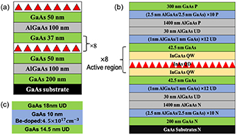
Figure 1. (a) The schema of InAs/GaAs QD test structures with direct Si-doping. (b) The schema of n-type doped and undoped QD laser structure. (c) The schema of the Be-doped GaAs spacer layer.
Download figure:
Standard image High-resolution image2.2. Laser material epitaxial growth
In order to compare the effect of different doping techniques on the laser performance, three laser structures were grown: Si n-type direct doping, Be p-type modulation doping and nominally undoped active material on GaAs substrates for simplicity. The rest of the laser structure, shown in figure 1(b), started with a 200 nm n-type doped GaAs buffer layer, followed by a ten-repeat Al0.4Ga0.6As/GaAs with 2.5 nm each. The following structure was an n-type doped 1.4 μm Al0.4Ga0.6As cladding layer and a 30 nm undoped Al0.4Ga0.6As guiding layer. The DWELL active structure separated by 42.5 nm GaAs spacer layer was deposited after a 12-repeat Al0.4Ga0.6As/GaAs waveguide. Si dopants were applied during the assembling process in QD formation with a doping density of 1.2 e/dot. The p-type modulation-doped sample with Be dopants is schematically shown in figure 1(c), where a 10 nm p-type doped GaAs spacer layer of ten holes per dot is embedded within a 42.5 nm GaAs spacing layer [39]. About 12 repeats of Al0.4Ga0.6As/GaAs waveguide is grown on the top of the DWELL active region, followed by a 30 nm of undoped Al0.4Ga0.6As layer and 1400 nm p-type doped Al0.4Ga0.6As cladding layer. A 300 nm highly p-type doped GaAs contact layer is grown on the top of the structure.
2.3. Laser fabrication
The laser devices were fabricated into mesa stripe lasers with 25 μm and 50 μm width mesas by conventional photolithography and wet chemical etching to a depth of 3.3 μm, which went through the active region layers. The p-contact was on top of the mesa, of width 20 µm and 45 µm respectively for the 25 µm and 50 µm wide mesas, was formed by 40 nm Ti and 300 nm Au which were deposited by E-beam evaporator. After lapping to around 100 μm substrate thickness, the Au/Ge/Ni N-contact was deposited on the backside of the sample. The as-cleaved facets were clean and mirror-like, which is easier to achieve when grown on GaAs substrates. Laser bars were cleaved with four different cavity lengths, of 0.5 1, 1.5 and 2 mm, and then mounted on indium-plated copper heatsinks using indium paste and wire-bonded to enable the following measurements.
3. Effects of direct Si-doping on InAs/GaAs QD
3.1. Characteristics of InAs/GaAs QDs with Si doping
The atomic force microscopy images of the inset of figure 2 show that the Si dopants have almost negligible influence on QD density, which are summarised in table 1, which summaries the QD densities, PL peak intensities, peak wavelength and full-width at ground-state half-maximum (FWHM). The QD densities are around 4.5 × 1010cm−2 in all images, as the inset of figure 2 shows.

Figure 2. PL results for all calibration samples at room temperature. Sample A, B, C, D denotes the InAs QD sample with Si doping densities of 0, 0.6, 1.2, 2.4 electrons per dot respectively. Inset: AFM images of InAs/GaAs QDs with different Si doping densities.
Download figure:
Standard image High-resolution imageTable 1. Summary of QD densities and PL characteristics of samples with different doping concentrations.
| Sample | Doping density | QD density (1010 cm−2) | PL peak intensity (a.u.) | Peak wavelength (nm) | FWHM (meV) |
|---|---|---|---|---|---|
| A | 0 | 4.50 | 5.116 | 1277 | 29.76 |
| B | 0.6 | 4.33 | 4.543 | 1288 | 31.43 |
| C | 1.2 | 4.49 | 6.563 | 1292 | 31.97 |
| D | 2.4 | 4.57 | 6.66 36 | 1303 | 35.70 |
The PL measurement was performed at room temperature with a 635 nm laser excitation in a Nanometrics RPM 2000 PL Mapper. The PL spectra in figure 2 prove that the Si dopants impact the peak characteristic of InAs/GaAs QDs. As the Si doping density increases, the peak wavelength redshifts and the FWHM increases. Such a result could have two causes. The presence of Si dopant during growth decreases the carrier lifetime, meaning that the carrier density is reduced for the same PL pumping. For a system in thermal equilibrium, this leads to an apparent spectral redshift and broadening. Alternatively, the presence of Si dopant during growth may have enhanced the QD inhomogeneity and increased the QD size. As for the PL intensity, the PL peak intensity decreases at first and then increases while the Si dopant density increases continuously, suggesting that at least for the higher doping level, any decrease in carrier lifetime is due to an enhanced radiative recombination rate. Considering the PL peak intensity and FWHM, a doping density of 1.2 e/dot as sample C is selected for the laser fabrication.
In order to interpret the impact of Si dopants, a representation of the dot and wetting layer valence states were calculated using NextNano for the undoped situation and where direct n-type doping into the dot material was used [40]. The results are shown in figure 3. Such calculations rely on various material parameters such as band offsets, which are not always universally agreed upon. Here typical literature values are used to illustrate the effects, including the decreased number of valence energy states within the dot.
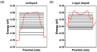
Figure 3. Schema of the calculated valence states of InAs/GaAs QD and wetting layer with undoped dots (left) and direct Si-doping (right). The two potentials have been aligned in energy such that the dot ground states align to allow the viewer to compare the number and spacing of the states. The n-dopant atom ionises and the resulting ion distorts the potential resulting in fewer valance states confined in the dot.
Download figure:
Standard image High-resolution imageAs shown in figure 3, the net result for the addition of Si-dopant atoms is to change the ground state (e1-h1), excited state (e2-h2) and second excited state (e3-h3) transition energies from 0.947, 1.021 and 1.128–0.940, 1.019 and 1.139 eV, which result in slightly longer wavelength emission for the n-type doped dots, as shown in table 1.
3.2. Characteristics of laser samples
The fabricated broad-area lasers were tested under pulsed mode (1 μs pulse, 0.5% duty circle). Figure 4 compares the single-side light-current (L-I) curves of n-type direct-doped, undoped and p-type modulation-doped lasers with a cavity length of 2 mm, a contact width of 20 μm and a mesa width of 25 μm. It can be clearly seen that the n-type direct doped QD laser possesses the lowest threshold current among all three laser types, while the threshold currents of the p-type modulation-doped lasers are much higher than those of the n-type doped and undoped structures. We determined threshold current density by measuring the device length and the device width by observing the width of the near field. Line scan measurements of the device near fields are plotted in figure 5. The nearfield profile of the n-type doped active region laser device is less than the metal contact width, suggesting significant gain/loss guiding in the n-type doped laser. From figure 5, it can be derived that the carrier distribution amongst the dots is very different for the n-type doped lasers.

Figure 4. Single-side pulse L-I curves of QD lasers with different doping types (active area of 25 μm × 2000 μm) at 300 K. The inset figure gives the lasing spectra of the direct n-type doped QD laser with an injection current of 62 mA (black), undoped QD laser with an injection current of 94 mA (red) and p-type modulation-doped QD laser with an injection current of 152 mA (blue) respectively.
Download figure:
Standard image High-resolution image
Figure 5. Line scan across the near field of the 3 laser types for samples that are 2 mm long with 25 µm wide mesa.
Download figure:
Standard image High-resolution imageThus, considering the difference in the near field results, the threshold current density was calculated and shown in figure 6 as a function of temperature for the above lasers. As figure 6 indicates, the threshold current densities of all three lasers increase as temperature increases. The p-type modulation-doped lasers show a relatively small change in threshold current density over the temperature range compared to the n-type doped and undoped laser. The undoped lasers have a lower threshold current density than the p-type modulation-doped ones at a low-temperature range. As temperature increases, the threshold current densities of the undoped and n-type doped lasers exceed the p-type modulation-doped laser, which shows the p-type modulation-doped laser possesses the highest characteristic temperature among the three lasers. Based on the threshold current density, the undoped and n-type doped lasers' characteristic temperatures were derived as 70.2 K and 74.0 K in the whole temperature range respectively, while the p-type modulation-doped laser had two characteristic temperatures in different temperature ranges, which was 414.9 K from 17 °C to 57 °C and 155.5 K from 57 °C to 97 °C respectively. The reduction in the relative temperature sensitivity of the p-type modulation-doped laser was even more relatively pronounced for shorter devices.

Figure 6. The dependence of the threshold current on temperature for the direct n-type doped, undoped and p-type modulation-doped lasers with the active region of 50 μm mesa × 2000 μm cavity length.
Download figure:
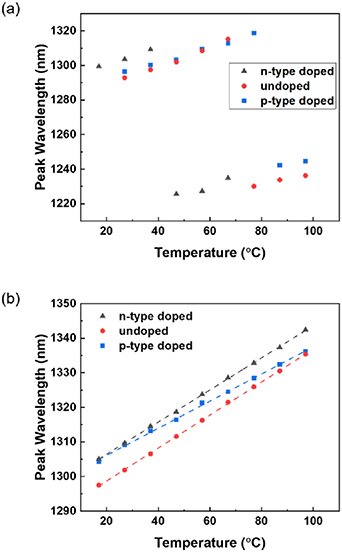
Standard image High-resolution imageWe investigated the peak wavelength as a function of temperature in the range 17 °C–97 °C for all lengths and mesa widths and results for 0.5 mm and 2 mm lasers are shown in figure 7. All devices with cavity lengths of 1 mm and above lase on the ground state across this temperature range. However, when the cavity became shorter, more gain is required to overcome the mirror loss. At some temperature this gain is first achieved at wavelengths corresponding to the excited state, meaning the laser is less useful for applications. P-type modulation doping causes the excited electron energy states to be relatively depopulated due to the excess of holes, so the quasi-Fermi levels are shifted towards the valence states, delaying the switch to excited state lasing. The inverse occurs in the n-type doped case. The direct n-type doped laser switched from ground to excited state lasing at an operating temperature of 47 °C, while the undoped and p-type modulation-doped lasers switched at 77 °C and 87 °C respectively.
Figure 7. The lasing wavelengths of three types of doping lasers from 17 °C to 97 °C (a) with a cavity length of 0.5 mm and 50 μm wide mesa. (b) With a cavity length of 2 mm and 50 μm wide mesa.
Download figure:
Standard image High-resolution image
4. Conclusion
We presented a study on the effect of the direct Si doping technique on high-density InAs/GaAs QDs grown on native substrates. High-performance InAs/GaAs QD lasers with un-intentional doped, p-type modulation-doped and direct n-type doped active regions were demonstrated. The Si dopants applied through the direct n-type doping method can reduce the threshold current density of InAs QD lasers and narrow the near field lasing spot, but they accelerate the lasing mode switch with a short cavity at a high operating temperature. In contrast, the p-type modulation-doped lasers will have a better performance at a higher temperature at the expense of increasing the threshold current density of the InAs QD lasers in the temperature range of 17 °C–57 °C.
Acknowledgments
The authors thank for the funding from the UK Engineering and Physical Sciences Research Council (EP/T01394X/1 and EP/P006973/1); National Epitaxy Facility; Royal Academy of Engineering (RF201617/16/28); European Project H2020- ICT-PICTURE (780930); National Key Research and Development Program of China (2021YEB2800500); National Nature Science Foundation of China (61574138, 61974131); Nature Science Foundation of Zhejiang Province (LGJ21F050001); Major Scientific Research Project of Zhejiang Lab (2019MB0AD01). L Jarvis thanks to COVID-19 Hardship Grant from the Rank Prize.
Data availability statement
The data that support the findings of this study are available upon reasonable request from the authors.