
Abstract
We investigate the effectiveness of laser-induced treatment as compared to rapid-thermal annealing (RTA) for the activation of p-type dopant in Mg-doped GaN layers. The study is based on a wide set of analytical techniques, including resistivity measurements, atomic force microscopy (AFM), scanning emission microscopy, dynamic secondary ion mass spectroscopy (SIMS), time-of-flight (TOF) SIMS and energy dispersive x-ray (EDX) spectroscopy in combination with scanning transmission electron microscopy (STEM). Samples are treated at different energy densities and in different atmospheres, to provide a comprehensive overview of the topic. The analysis is carried out on GaN-on-Si samples, to demonstrate the effectiveness of the treatment even in presence of high threading dislocation densities. The original results presented in this paper indicate that: (a) laser treatment is an effective process for activating the p-type dopant in Mg-doped GaN layers; even at low irradiation energy densities (400 mJ cm−2) the laser treatment can effectively activate the Mg doping, with the best resistivity results obtained (around 1.5 Ωcm) comparable with those obtained by optimized RTA; (b) resistivity varies with temperature with activation energy Ea = 0.14 eV, which is compatible with the MgGa acceptor in GaN; (c) TOF-SIMS, AFM, EDX-STEM analysis indicates that the laser treatment does not modify the concentration profile of magnesium and surface roughness for low and moderate laser energy densities; changes are detected only for energy densities above 600 mJ cm−2, for which a significant degradation of the surface is revealed. The experimental evidence collected within this paper provide an accurate assessment of the process conditions for effective laser activation of Mg-doped GaN, thus allowing the fine-tuning required for selective activation and for industrial applications.
Export citation and abstract BibTeX RIS

Original content from this work may be used under the terms of the Creative Commons Attribution 4.0 license. Any further distribution of this work must maintain attribution to the author(s) and the title of the work, journal citation and DOI.
1. Introduction
GaN is a wide bandgap semiconductor, with an energy gap equal to 3.4 eV. When using impurity doping, the ability of obtaining a high free charge density strongly depends on the binding energy of the donors and acceptors, i.e. on their energetic position with respect to the conduction and valence band ( and
and  , respectively). With regard to donors, GaN has a relative shallow impurity (Si), with an activation energy of 0.015 eV [1], so it is relatively easy to reach carrier densities in the range of 1018 cm−3 and above. On the contrary, the most commonly used acceptor is Mg, having a relatively large binding energy that has been estimated to be in the range 0.12–0.16 eV, depending on the doping level. The fraction of ionized acceptors
  can be calculated as [2]:
and strongly depends on the term  , where
  is the degeneracy factor (for an acceptor level in GaN is usually used the unoccupied-state degeneracy
  = 4 and the occupied-state degeneracy
  = 1),
= 1),  the effective density of states in the valence band at 1 K and Ea the acceptor ionization energy defined as the difference between the acceptor energy level and the valence band. Figure 1 represents the variation of the ionized acceptors as a function of the doping level: it is clear that to achieve free hole densities above 1018 cm−3 is not straightforward and requires to introduce a large Mg concentration (>1019 cm−3).

Figure 1. Variation of the fraction of ionized acceptors as a function of the acceptors concentration for different ionization energy values according to [2].
Download figure:
Standard image High-resolution imageThe difficulty of p-type doping in GaN is further exacerbated by the fact that, after growth by metal-organic chemical vapor deposition (MOCVD), Mg-doped GaN layers are highly resistive, due to the inactivation of Mg acceptors induced by the formation of Mg–H complexes [3]. To activate the acceptor dopant, an additional processing step is required: the most explored approaches have been low-energy electron beam irradiation [4], and rapid-thermal annealing (RTA) in nitrogen atmosphere, at temperatures above 600 °C [5]. The latter approach is now widely adopted at industrial level, since it allows fast and effective activation on wafer scale.
Achieving high p-GaN conductivity is fundamental for both optoelectronic (light-emitting diodes, laser diodes) and electronic (high-electron mobility transistors (HEMTs), vertical transistors) GaN-based devices. For this reason, alternative methods are explored, with the aim of obtaining a good activation rate, and—whenever possible—spatially-resolved activation. One of the proposed methods is laser activation [6–8]: the idea is to use a short-wavelength excimer laser with ns-range pulses to irradiate the semiconductor in controlled atmosphere. The energy released by the short pulses results in a localized and effective dissociation of the Mg–H complexes, with consequent increase in p-GaN conductivity. A stage can be used to move the sample in x, y and z-direction, thus controlling the size and position of the irradiated area.
Laser-based Mg-activation has been proposed in early reports [9–12], but no extensive investigation of the experimental conditions and processing parameters has been presented at the time, since in the early 2000s the study of GaN devices was still in an early phase and RTA was sufficient for developing optoelectronic devices.
Now the context has significantly changed, since the fabrication of optimized p-GaN layers is fundamental also for the development of HEMTs, vertical diodes and MOSFETs. For these devices, it can be important to develop methods for an effective activation of specific p-GaN layers, while leaving others regions inactivated. An example is the creation of current-confinement regions, i.e. of carrier blocking areas to control the flow of current in specific regions of the devices. For the fabrication of confinement layers, crystal regrowth and ion implantation can be used; however, both methods have disadvantages, such as the need to interruption of crystal growth [13] and the control of implantation damage, with consequent need of ultra-high-pressure annealing [14].
In a recent paper [6], Kurose et al provided experimental proof of the effectiveness of laser-induced local activation of Mg-doped GaN, thus confirming the important of this technology for the fabrication of vertical and lateral GaN devices, as an alternative to regrowth and ion implantation. This recent report demonstrated the importance of laser-based p-GaN activation, but did not give further information on the physics of laser-based p-GaN activation, and on how to tune the process parameters to optimize the effectiveness of the treatment.
The goal of our paper is to significantly improve the understanding of laser activation of p-GaN, based on an extensive analysis carried out by resistivity vs temperature measurements, secondary ion mass spectroscopy (SIMS), atomic force microscopy (AFM), time-of-flight (TOF)-SIMS and energy dispersive x-ray (EDX)-scanning transmission electron microscopy (STEM).
The results obtained by laser annealing are systematically compared to those of RTA, showing that even at low irradiation energy densities (400 mJ cm−2) the resistivity values obtained (around 1.5 cm) are comparable to those obtained by optimized RTA. In addition, we show that resistivity has an activation energy equal to Ea = 0.14 eV, which is in agreement with the current estimates for MgGa acceptor in highly doped GaN [2], demonstrating that Mg activation gives the dominant contribution to conductivity. Furthermore, by TOF-SIMS and AFM we demonstrate that the laser activation does not modify the concentration profile of magnesium and surface roughness for low and moderate laser energy densities. Additionally, the H-concentration profile leads to assumption, that the treatment duration is sufficiently long to dissociate Mg–H complexes, and relatively short for out-diffusion of H.
Significantly, we chose to carry out the analysis on samples grown on a silicon substrate, in order to evaluate the effectiveness of the treatment in a worst case scenario, where high dislocation densities can promote impurity diffusion during treatment.
2. Experimental details
Mg-doped GaN layers were grown in an AIXTRON G5+ C Planetary® MOCVD reactor in a 5 × 200 mm configuration. The growth was performed on 200 mm, 1150 µm thick Si <111> substrates. Following an AlN nucleation layer, an AlGaN-based strain relief layer was grown after which 3 µm GaN was deposited. On top, 200 nm pGaN was grown with a nominal doping density of 4 × 1019 cm−3 (see figure 2 for a schematic representation of the analyzed samples). The samples were not subjected to an in situ anneal, in order to submit them to RTA and laser annealing, as discussed in the following. Full-width half-maximum x-ray diffraction rocking curves gave values of 390 arcsec in the wafer center and 395 arcsec at the wafer edge for the GaN <002> peak, and around 450 arcsec for the GaN <102> peak for both center and edge.
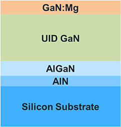
Figure 2. Epitaxial structure of the samples under test.
Download figure:
Standard image High-resolution imageLaser activation was performed by means of an excimer KrF laser system emitting at 248 nm. The number of pulses was set to 10 with a repetition rate of 1 Hz, while the energy density of each pulse has been ranged from 400 to 700 mJ cm−2. The laser beam was homogenized and shaped along the beam path through a set of lenses and finally focalized on a square spot of 5 mm × 5 mm with 2% uniformity. The experiments were carried out in air and in nitrogen atmosphere.
TOF-SIMS measurements were performed in negative and positive polarity using an IONTOF TOF-SIMS M6 instrument. For each measurement, an area of 100 µm by 100 µm of the sample was analyzed. As the residual gas in the vacuum chamber contains H, the measurement in negative polarity was performed after approximately 3 d in vacuum (3 × 10⁻¹⁰ mbar vacuum pressure) to obtain a low background signal. Each measurement was performed twice to account for inhomogeneities of the sample. The deviations between both measurements were negligible, showing high reliability and reproducibility of the measurement. The Mg-signal in positive polarization was normalized to the Ga-signal. To determine Mg- and H-concentrations, a sample with known Mg- and H-concentrations was measured and used for calibration using a relative sensitivity factor. For the visualization of the depth profiles, an average adjacent point compression of ten was used.
3. Results
3.1. RTA
To obtain a reference, we started by submitting the analyzed samples to RTA. This allowed us to evaluate the best resistivity that can be obtained via the standard procedure, to be used for a comparison with laser activation.
The GaN:Mg films were activated in N2 ambient for 10, 20 and 30 min with varying temperatures of 650 °C, 750 °C and 850 °C. To analyze the electrical properties of the Mg-doped GaN films, resistivity measurements were carried out in van der Pauw configuration. Figure 3(a) shows a comparison of the bulk resistance of activated Mg-doped GaN in the three conditions. RTA at 650 °C induced a decrease of p-GaN resistivity to 6 Ωcm after 30 min. A stronger activation (down to ∼1.5 Ωcm) was obtained with higher temperatures (850 °C), and this value remained nearly constant as a function of treatment time. These values are comparable/lower than the 2 Ωcm reported by Nakamura et al [5], confirming that our treatment and semiconductor can reach similar levels of activation to what reported in the literature.
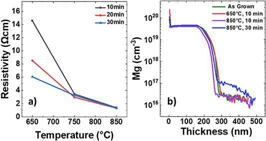
Figure 3. (a) Bulk resistance of Mg-doped GaN activated by RTA in N2 ambient for 10, 20 and 30 min with varying temperatures of 650 °C, 750 °C and 850 °C. (b) SIMS profile of samples submitted to in situ annealing at 800 °C and consequent RTA in N2 ambient at 650 °C for 10 min, 850 °C for 10 min and 850 °C for 30 min. No significant modification in the SIMS profiles is noticed after RTA.
Download figure:
Standard image High-resolution imageSIMS analysis was carried out to assess the stability of the elements, by comparing the best and the worst activation conditions (10 min at 650 °C and 30 min at 850 °C). As can be noticed in figure 3(b), the treatment at 650 °C, 10 min did not result in modifications in the SIMS profile. On the other hand, after treatment at 30 min at 850 °C a slight increase of the Mg signal towards the undoped region was observed. In principle, this could be ascribed to a back-diffusion of Mg, or to a worsening of the properties of the surface, that degrades the accuracy of the SIMS profiling.
However, AFM measurements (figure 4) revealed that RTA these three conditions did not result in an increased roughness of the material, since the RMS roughness was found to be in the range between 400 pm and 500 pm. This suggests that the slight increase in Mg concentration for the sample treated for 30 min at 850 °C can be ascribed to a minor back diffusion of Mg. Mg redistribution was reported also in previous reports (see [15] and references therein) at similar temperature levels, indicating the consistency of our results.

Figure 4. AFM measurements results of samples submitted to RTA treatment at different conditions in N2 ambient and correlated roughness values.
Download figure:
Standard image High-resolution imageIn our work, the highly resistive Mg-doped GaN samples were irradiated by a pulsed KrF ∼ 248 nm under two different gas atmospheres, ambient air and nitrogen, and investigated as a function of the laser energy density. The number of the KrF excimer laser pulses is fixed at 10 and the repetition rate is equal to 1 Hz. The electrical activation of GaN:Mg was ascertained by resistivity measurements in van der Pauw geometry. The bulk resistivity as a function of the laser energy density in air and in nitrogen-atmosphere is depicted in figures 5(a) and (b), respectively. As can be noticed, samples irradiated in air showed a resistivity comparable to RTA for high energy densities (>600 mJ cm−2), while for lower densities the treatment was found to be less effective.
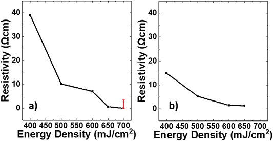
Figure 5. Resistivity measurements results after laser annealing treatment in ambient air (a) and nitrogen (b) at different energy densities.
Download figure:
Standard image High-resolution imageOn the contrary, the laser treatment in nitrogen atmosphere was found to be effective in the whole analyzed range (from 400 mJ cm−2–650 mJ cm−2). At 500 mJ cm−2 the resistivity was found to be equal to 5.2 Ωcm, while at 600 mJ cm−2 a value of 1.5 Ωcm was measured. This last value is comparable to what we obtained by the best RTA conditions and lower than the RTA data published in previous reports [5], demonstrating the effectiveness of the adopted process. Instead, the results obtained after treatment at 650–700 mJ cm−2 are not considered to lead to a reliable sample treatment, since, according to figures 6 and 8, the morphology is significantly degraded and can lead to the formation of metaling Ga/Mg phases at the surface. In according to this, only lower levels of irradiation have been considered effective in the analysis. The difference between the results obtained in air and in nitrogen atmosphere can be explained by a probable surface oxidation of the material, as proposed by Kim et al [9, 16].

Figure 6. Surface morphology of representative samples (untreated, and treated in nitrogen atmosphere at 400 mJ cm−2 and 600 mJ cm−2). For the sample analyzed at 600 mJ cm−2, two images are shown (5 × 5 μm2 and 20 × 20 μm2).
Download figure:
Standard image High-resolution imageThese results indicate that laser irradiation in nitrogen ambient is effective in activating Mg acceptors in GaN films on Si substrates; it is also clear that—similarly to the RTA case—nitrogen atmosphere is a key requirement to improve the p-type conductivity.
To compare laser activation with the RTA process, a detailed analysis of material morphology was carried out by AFM. Figure 6 shows the surface morphology of representative samples not-irradiated, irradiated in nitrogen atmosphere at 400 mJ cm−2 and at 600 mJ cm−2. Figure 7 reports the RMS surface roughness after laser annealing at different energy densities in N2 ambient. While the surface morphology presents no differences between the untreated and the 400 mJ cm−2—treated sample, structural properties were significantly degraded when increasing the laser density energy to 600 mJ cm−2. The high laser density energy promotes the formation of island-like surfaces, as visible also from the 20 × 20 µm2 view of the samples irradiated at 600 mJ cm−2. As shown in figure 7, the roughness value is constant for energy lower than 500 mJ cm−2, indicating that these conditions allow the enhancement of p-type conductivity without surface modifications. With increasing density energy, the surface roughness increases. This effect is ascribed to a laser ablation effect, as preliminarily suggested for GaN:Mg samples on sapphire substrates [9, 16].
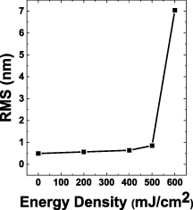
Figure 7. Root-mean-square roughness values of samples irradiated in nitrogen atmosphere at different energy values, from 100 to 700 mJ cm−2.
Download figure:
Standard image High-resolution imageComplementary information was obtained via scanning emission microscopy, and a detailed description is given in figure 8 (we only show results obtained at 600–700 mJ cm−2, i.e. those for which modifications have been detected). The formation of the island-like features is visible, for energy densities above 600 mJ cm−2.
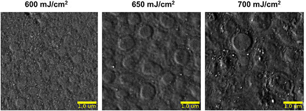
Figure 8. Scanning electron microscopy images of samples irradiated in nitrogen atmosphere between 600 and 700 mJ cm−2.
Download figure:
Standard image High-resolution imageBased on the results described above, we can conclude that laser activation of p-GaN is effective both in terms of device resistivity and in terms of surface morphology, for moderate pulse energy densities, in the range 400–500 mJ cm−2.
3.2. TOF-SIMS measurements
TOF-SIMS measurements of an untreated sample and for energy densities of 400, 500, 600 and 700 mJ cm−2 in N2 ambient were performed in negative and positive polarity to investigate the influence of the laser treatment on Mg and H content, as well as to search for any process related impurities.
Figure 9 shows the Mg depth profiles of an untreated sample, together with the irradiated ones. For all samples, an increase of the Mg concentration towards the surface can be observed. The concentration is then decreasing and reaches a plateau between 20 nm and 140 nm. Between 140 and 160 nm the Mg concentration starts to decrease again, and reaches the detection limit at 300 nm (except for an energy density of 700 mJ cm−2). No substantial differences in the Mg-depth profiles for the untreated sample and up to energy densities of 500 mJ cm−2 are observed, indicating that laser treatment at moderate energy densities does not favor instabilities in the Mg profile. For 600 mJ cm−2 the Mg concentrations starts to decrease earlier compared to the untreated samples and reaches into uid GaN layer, which can be explained by back diffusion of Mg as observed for the RTA treated samples.
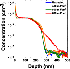
Figure 9. TOF-SIMS magnesium depth profile for an untreated sample together with the ones of laser irradiated samples in N2 ambient with different energy densities, 400, 500 and 600 mJ cm−2.
Download figure:
Standard image High-resolution imageTo evaluate the effect of the laser irradiation on the hydrogen signal, TOF-SIMS measurements in negative polarity are performed (figure 10). The hydrogen depth profile of the untreated sample is comparable to the ones of irradiated samples with an energy density up to 500 mJ cm−2, showing an approximately constant plateau for the first 180 nm. For an energy density of 600 and 700 mJ cm−2, an increase of the hydrogen signal towards the surface is observed as well as a broadening of this effect towards deeper layers. Only for energy density of 700 mJ cm−2 the H plateau is substantial lower compared to the other samples. The H concentration of the plateau for energy densities up to 600 mJ cm−2 was determined to be between 2.2 and 2.9 × 10¹⁹ atoms cm−3 (with an error of approximately 25%). Since only minor differences in the H signal up to 600 mJ cm−2 are observed, although the electrical resistivity shows an activation of Mg, we conclude that the Mg–H complexes are broken, but that the activation time is too short for an out diffusion of the H. After Mg–H dissociation, hydrogen is supposed to remain present in the semiconductor, and creates bonds to defects (like vacancies) or form molecular hydrogen.
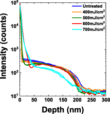
Figure 10. TOF-SIMS hydrogen depth profile for an untreated sample together with the ones of laser irradiated samples in N2 ambient with different energy densities, from 400 up to 700 mJ cm−2.
Download figure:
Standard image High-resolution imageTo investigate the incorporation of impurities by the laser treatment, the oxygen depth profiles are compared (figure 11). For some measurement, spots with higher O signal were visible in cumulated elemental maps, probably caused by surface contamination independent of the laser irradiation, and therefore they have been excluded in the comparison displayed. Up to an energy density of 400 mJ cm−2, the irradiated samples profiles present no deviation to the one of untreated sample. Starting from 500 mJ cm−2 the formation of an oxygen-rich surface layer can be observed, which becomes thicker for higher energy densities. These results are in good agreement with the AFM and SEM investigations, showing only minor surface changes for energy densities up to 500 mJ cm−2.
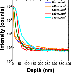
Figure 11. TOF-SIMS oxygen depth profile for an untreated sample together with the ones of laser irradiated samples in N2 ambient with different energy densities, from 400 up to 700 mJ cm−2.
Download figure:
Standard image High-resolution imageSummarized, the TOF-SIMS results show, that moderate pulse energy densities, in the range 400–500 mJ cm−2 have no strong impact on the Mg, H and O depth profiles.
In order to investigate the impact of the laser treatment on the sample surface, the STEM energy dispersive x-ray spectroscopy (EDXS) analysis of different samples cross section was performed. This analysis was carried out on samples that were first in situ annealed at 800 °C and then laser irradiated in nitrogen atmosphere, with different energy densities, from 100 up to 650 mJ cm−2, assuming the surface behavior similar to those without the pre in situ annealing. Results depicted in figure 12 reveals that the untreated sample and the ones irradiated with an energy density up to 200 mJ cm−2 present a similar behavior, showing an homogenous oxygen layer of approximately 2.5 nm, while at 650 mJ cm−2, the oxygen rich layer is inhomogeneous and of approximately 6–8 nm. This is in good agreement with the results of TOF-SIMS oxygen depth profile for energy densities higher than 500 mJ cm−2 (figure 11). Although the laser irradiation was performed under N2 atmosphere, a thick O layer was formed possibly due to residual oxygen present within the GaN surface layer or during the laser treatment.
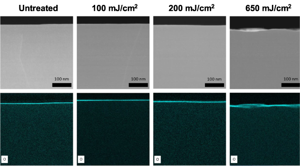
Figure 12. HAADF-STEM images and EDXS elemental maps of oxygen for cross sections of different samples: untreated and laser irradiated in N2 ambient at different energy densities: 100, 200 and 650 mJ cm−2. Each sample is submitted to a pre in situ annealing at 800 °C.
Download figure:
Standard image High-resolution image3.3. Further improvements to the process and temperature-dependent characterization
To further enhance p-type conductivity, we evaluated the effect of increasing the number of pulses used for laser activation, while maintaining a low energy density, with the aim of preventing damage to the surface. Based on the AFM analysis reported above, we carried out an analysis in nitrogen atmosphere with energy density of 400 mJ cm−2, and number of pulses between 5 and 1000. The results (figure 13) show that with increasing pulse number a significant decrease in resistivity can be obtained, starting from 24 Ωcm for five pulses, down to ∼2 Ωcm for 300–1000 pulses. This last value is comparable to the 2 Ωcm reported by Nakamura et al [5], indicating that the repetition of low energy density pulses can be as effective as RTA.
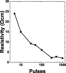
Figure 13. Resistivity measurements results after a variable number of laser pulses between 5 and 1000, for a laser energy density of 400 mJ cm−2 in nitrogen atmosphere.
Download figure:
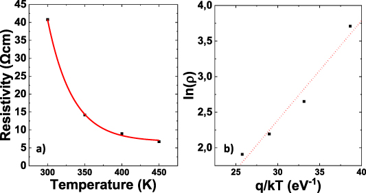
Standard image High-resolution imageFinally, we evaluated the temperature-dependence of resistivity of laser-activated samples. Figure 14(a) represents the bulk resistivity as a function of temperature, from 300 K up to 450 K relative to the sample activated with 400 mJ cm−2 in nitrogen atmosphere. The resistivity has an exponential dependence with temperature and the correlated Arrhenius plot (figure 14(b)) led to an estimate of the activation energy of the Mg dopant of 0.14 eV. This value, for the Mg-acceptor concentration of this study (NA = 4 × 1019 cm−3), is in good agreement with the experimental results from literature ([2] and references therein).
Figure 14. (a) Temperature dependence of the bulk resistivity after laser treatment in nitrogen rich atmosphere at 400 mJ cm−2 and related Arrhenius plot (b).
Download figure:
Standard image High-resolution image
4. Conclusions
In summary, we investigate the effectiveness of laser-induced treatment as compared to RTA for the activation of p-type dopant in Mg-doped GaN layers. The study is based on a wide set of analytical techniques, including resistivity measurements, AFM, SEM, dynamic SIMS, TOF SIMS and EDXS in combination with STEM. Samples are treated at different energy densities and in different atmospheres, to provide a comprehensive overview of the topic. The analysis is carried out on GaN-on-Si samples, to demonstrate the effectiveness of the treatment even in presence of high threading dislocation densities.
Acknowledgments
This activity has received funding partially from the ECSEL Joint Undertaking (JU) under Grant Agreement No. 826392, Ultimate GaN. The JU receives support from the European Union's Horizon 2020 research and innovation programme and Austria, Belgium, Germany, Italy, Slovakia, Spain, Sweden, Norway, Switzerland. This project is co-funded by the Ministry of Education, Universities and Research in Italy.
Laser activation was available thanks to the infrastructure acquired through the grant UNIPD-ISR 2017 'SENSITISE' at the University of Padova.
Data availability statement
The data that support the findings of this study are available upon reasonable request from the authors.