
Abstract
Semiconductor mode-locked lasers (MLLs) with extremely high repetition rates are promising optical frequency comb (OFC) sources for their usage as compact, high-efficiency, and low-cost light sources in high-speed dense wavelength-division multiplexing transmissions. The fully exploited conventional C- and L- bands require the research on O-band to fulfil the transmission capacity of the current photonic networks. In this work, we present a passive two-section InAs/InGaAs quantum-dot (QD) MLL-based OFC with a fundamental repetition rate of ∼100 GHz operating at O-band wavelength range. The specially designed device favours the generation of nearly Fourier-transform-limited pulses in the entire test range by only pumping the gain section while with the absorber unbiased. The typical integrated relative intensity noise of the whole spectrum and a single tone are −152 and −137 dB Hz−1 in the range of 100 MHz–10 GHz, respectively. Back-to-back data transmissions for seven selected tones have been realised by employing a 64 Gbaud four-level pulse amplitude modulation format. The demonstrated performance shows the feasibility of the InAs QD MLLs as a simple structure, easy operation, and low power consumption OFC sources for high-speed fibre-optic communications.
Export citation and abstract BibTeX RIS

Original content from this work may be used under the terms of the Creative Commons Attribution 4.0 license. Any further distribution of this work must maintain attribution to the author(s) and the title of the work, journal citation and DOI.
1. Introduction
The optical frequency combs (OFCs) with a straightforward connection between optical and microwave domains are used in numerous fields, such as medical diagnostics [1], atomic clock distribution/recovery [2], precision measurements [3–5], gas spectroscopy [6, 7], and optical communications [8–12]. To support such a broad application divergence, the last two decades have witnessed an expansion of the laser-based comb technology [13, 14]. There are various OFC generation mechanisms, including gain switched comb, nonlinear fibres, microresonator systems, electro-optic comb generators, and mode-locked lasers (MLLs). Among all technologies, the MLLs, particularly the semiconductor MLLs, are considered the most promising light sources in future photonic integrated circuits (PICs) owing to their simplification, compactness, easy-operation, low power consumption, and high wall-plug efficiency [9, 15].
Although, quantum-well materials have been intensively investigated over the last two decades. The quantum-dot (QD) material, benefits from a broader inhomogeneous gain spectrum, an ultrafast carrier dynamic [16], together with other inherent features like low threshold current [17], temperature resilience [18, 19], high tolerance to defects and optical feedback [28, 29] have attracted increasing attentions and offered opportunities for future complementary metal-oxide-semiconductor (CMOS)-compatible PIC technology [30–34].
During the past decade, the ever-growing demand for data transmission capacities have inspired the research in dense wavelength-division multiplexing (DWDM) technology. The ITU-T G.694.1 recommendation has proposed a variety of fixed channel spacings ranging from 12.5 to 100 GHz in DWDM applications. While the MLLs-based OFC sources with a larger mode-spacing (⩾100 GHz) are more desirable in the DWDM transmission systems for the potentially reduced number of light sources required, it is challenging to obtain the needed high gain in an ultimate short cavity, especially for QD materials devices. Given that, most previous QD-based mode-locked OFC studies (as summarised in table 1) have either involved complex high order harmonics [21, 27], or employed complicated system-level setups [25] for large mode-spacing OFC generations. It is notable that most high-performance devices operate at the telecom C-band, while the devices working at telecom O-band are still relatively immature, suffering from a lower modal gain and a broader pulse duration. Furthermore, the conventional C-band has been extensively exploited, the current state-of-the-art high-speed transmission system requires the use of telecom O-band to boost the transmission capacity of existing photonic networks [35].
Table 1. Summary of QD-based mode-locked OFC source with an ultrahigh repetition rate.
| Telecom band | Repetition rate(GHz) | Material | Methods | Pulse duration (ps) | −3 dB bandwidth (nm) | TBP | Year/references | |
|---|---|---|---|---|---|---|---|---|
| Gaussian | Sech2 | |||||||
| C-band | 134 | InGaAsP/InAs QDash | Single section | 0.8 | 4.3 | 0.46 | — | 2006/[20] |
| O-band | 117 | InGaAs QD | CPM-3rd harmonic | 2.14 | — | — | 0.39 | 2006/[21] |
| 238 | CPM-6th harmonic | 1.3 | — | — | 0.33 | |||
| C-band | 92 | InAs/InP QD | Single section | 0.312 | 11.62 | 0.457 | — | 2008/[22] |
| C-band | 10–100 | InAs/InP QD | Single section | 0.295 | 17.9 | 0.66 | — | 2010/[23] |
| 437 | FBGs | 0.810 | — | — | — | |||
| O-band | 100 | InGaAs/GaAs QD | Mode-selections | — | — | — | — | 2010/[24] |
| O-band | 100 | InGaAs/GaAs QD | Fabry–Perot Etalon | — | — | — | — | 2011/[25] |
| O-band | 102 | QD | CPM-6th harmonic | — | — | — | — | 2018/[26] |
| O-band | 100 | Chirped QD | CPML-5th harmonic | 2.3 | — | — | — | 2019/[27] |
| O-band | 94 | InGaAs/GaAs QD | Two-section | 0.69 | 3.18 | 0.45 | — | This work |
Considering all points listed above, in this work, we report a passively QD MLL-based O-band transform-limited OFC source generated at ∼100 GHz fundamental repetition rate with sub-picosecond pulse durations. By optimising the growth conditions, a QD active region with high dot density (5.9 × 1010 cm−2) and good uniformity is accomplished, providing a room-temperature PL full width at half-maximum (FWHM) as low as 28 meV. During the whole test range, nearly Fourier-transform-limited Gaussian-pulses with ∼100 GHz mode-spacing are realised throughout. The typical integrated average relative intensity noise (RIN) values of the whole spectrum and a single tone, average between 100 MHz and 10 GHz, are −152 and −137 dB Hz−1, respectively. Moreover, the transmission ability of this laser is evaluated by carrying out a 64 Gbaud four-level pulse amplitude modulation (PAM-4) back-to-back (B2B) transmission for seven independent channels. The corresponding measured bit error ratios (BERs) confirm the possibilities for such OFC source usage in high-speed data centre applications. Our results suggest the proposed two-section QD MLL is a powerful candidate for simple structure, low-cost, high efficiency and integrable DWDM light sources.
2. Material and device design
The devices presented in this paper were prepared by solid-state molecular beam epitaxy, with emission wavelength in the 1.3  m range. A self-assembled InAs QD structure was grown on a Si-doped GaAs (001) surface together with AlGaAs cladding layers. Here, a high-quality 300 nm Si-doped GaAs contact layer was first developed, followed by the lower cladding layer that consists of n-type Al0.2Ga0.8As/Al0.4Ga0.6As/Al0.2Ga0.8As in a thickness of 20 nm/1400 nm/20 nm, respectively. Then, the active region containing an eightfold layer stack of InAs QDs was situated in the centre of the lower and upper cladding layers. The upper cladding layer was comprised of p-type Al0.2Ga0.8As/Al0.4Ga0.6As/Al0.2Ga0.8As in a thickness of 20 nm/1400 nm/20 nm. After depositing a heavily p+-doped 300 nm thick GaAs contact layer above the upper cladding layer, the entire growth procedure was completed. As known, a high optical gain is a prerequisite for ultra-high repetition rate pulse generation in a two-section passively MLL. To this end, an extraordinary design is utilised in the active region to improve the material's performance. The inset of figure 1(a) shows the cross-sectional TEM image of the active region. A larger than a usual number of QD layers (eight layers in total) was employed to obtain the desired high optical gain. Instead of using the conventional dot-in-a-well structure, here, the QDs were self-assembly formed by depositing three monolayers of InAs directly on the GaAs surface. Then, the initial QDs were covered by a 3.7 nm strain-reducing layer made of InGaAs. Such strain-reduced QDs could promise the light emission at the range of 1.3
  m, maintain the high QD density while preserving the QDs uniformity [36, 37]. The profile of a single dot can be extracted from the zoom-in window, where a high-resolution TEM image showing a truncated pyramidal shaped QD with a base length of 20–25 nm and a height of 6–8 nm. As a result, an ultrahigh dot density of 5.9 × 1010 cm−2 (nearly double the previous result of 3 × 1010 cm−2 [38]) is finally accomplished in this multi-layer structure with no degradation in QD uniformity. The room-temperature PL emission spectrum with a narrow linewidth of 28 meV is displayed in figure 1(a), indicating a minor variation in size and shape of inhomogeneous QDs in this work.

Figure 1. (a) The room-temperature photoluminescence (PL) emission spectrum of the sample. (Inset: the cross-sectional transmission electron microscopy (TEM) image of the active region and a single dot (zoom-in)). (b) Schematic of the unbiased passively two-section MLL.
Download figure:
Standard image High-resolution imageThe schematic diagram of the device under investigation is presented in figure 1(b). The 5  m wide two-section MLLs were processed from the wafer described above with standard fabrication methods, including semiconductor dry etching and metal/dielectric deposition techniques. Based on the previous study with a similar structure in [19], a group effective index of 3.7 can be found. To realise ∼100 GHz mode-spacing, the total cavity length of the lasers was set to be 405
  m, 14% (56.7 μm) of which formed the saturable absorber (SA) section. Such design could provide us with a comparable high differential loss in the SA section and a relatively small differential gain in the gain section, resulting a high gain-to-SA saturation energy ration in this extremely short cavity device. A citric-acid solution was used to selectively remove a width of 10
  m of the heavily doped p-type contact GaAs layer between the gain and SA sections, achieving an electrical isolation resistance of around 2.5 kΩ. After thinning the backside to 120
  m, a high-reflective coating of 95% was applied on the facet close to the SA section while the facet near the gain section was left to as-cleaved. Then, the lasers were mounted p-side up on an indium-plated copper heat sink and gold-wire-bonded to enable electrical contacts. Finally, the devices were packaged with a thermoelectric temperature controller (TEC) controller to fix the heat sink temperature at 20 °C. It is worth mentioning that, mode-locking (ML) phenomenon was obtained without reversed bias applied to the SA section, therefore, those unbiased two-section devices were packaged similarly to a single-section self-mode-locked (SML) laser since the minimal absorption will not affect the self-ML mechanism [39, 40].
3. Characterisation and discussion
3.1. Mode-locking (ML) performance
The MLLs used in this experiment operating as SML lasers since their SA sections were left floating [41]. To study their behaviours, the output spectrum was measured using an optical spectrum analyser (OSA) (Yokogawa AQ6370D or APEX AP2087A), and the pulse width was recorded with APE pulseCheck autocorrelator. Figure 2 summarises the representative continuous-wave characteristics of fabricated devices at room temperature. The measured light–current–voltage (L–I–V) curve is displayed in figure 2(a). The L–I curve presents the dependence of the average power received by a broad area detector on the bias current for gain sections, where 20 mA threshold current ( ) and 17.7% slope efficiency is exhibited. The test is stopped at 80 mA, taking into account the strong possibility of a damaged ultra-short cavity laser under a high-power density condition. As noticed, when injected current (
 ) increases from the
  , output power increases; when
  decreases after reaching the maximum value, the laser power decreases, but it persists even if
  . This results in a hysteresis loop near the
  , indicating the bistability of these devices [32]. As for the I–V curve, it exhibits a typical behaviour of a semiconductor laser where the voltage increases gradually with increased
  .
.
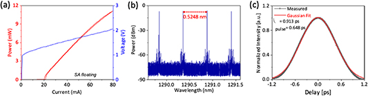
Figure 2. Two-section unbiased QD MLL basic characterisation at room temperature: (a) continuous wave L–I–V curve with SA floating. (b) High-resolution optical spectrum for adjacent channels (resolution: 0.04 pm). (c) Autocorrelation trace with Gaussian pulse fitting.
Download figure:
Standard image High-resolution imageThe mode-spacing of adjacent tones, i.e. the repetition rate of the device, is evaluated through apex OSA with a 0.04 pm resolution. In figure 2(b), the optical spectrum of four tones located near the central wavelength of 1291 nm at 66 mA is shown. A mode-spacing of 0.5248 nm is obtained, corresponding to a fundamental repetition rate of 94.6 GHz. To the best of our knowledge, this is the highest fundamental mode-spacing ever-achieved by a single QD-MLL in telecom O-band. Figure 2(c) shows the autocorrelation signal of an isolated pulse under the same bias condition to confirm the ML regime. The measured pedestal-free pulse profile is in good agreement with the fitted Gaussian pulse shape and gives a 648 fs deconvolved pulse duration without any external pulse compression scheme.
Figure 3(a) highlights the trends observed in the OSA spectrum evolution for  increment. The observations are refined and presented more visually in figure 3(b). By increasing the
  from 20 to 80 mA, a continuously red-shift of centre wavelength (from 1288 to 1293 nm) can be seen, confirming sustained ground state lasing. Meanwhile, the OSA spectrum tends to become a multipeak structure with an additional peak occurs in the high-frequency side due to an increased degree of self-phase modulation with increasing carrier density [42]. Hence, resulting in a steady expansion of OSA 3 dB bandwidth (from 1.6 to 4.3 nm).
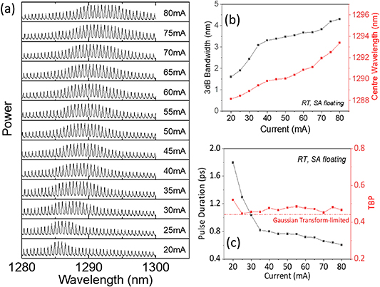
Figure 3. Room-temperature characteristics of two-section unbiased passively QD MLL with SA floating and  from 20 to 80 mA. (a) Optical spectra (resolution: 0.02 nm). (b) Spectral width and centre wavelength in (a). (c) Pulse duration and corresponding calculated TBP value.
Download figure:
Standard image High-resolution imageThis phenomenon has also been reported by other research groups [32, 43]. And we believe such a current-induced red-shift tendency could be minimised by carefully tailoring the structure of QDs [44, 45]. The corresponding pulse-duration obtained at each current level together with the calculated TBP values are given in figure 3(c). Considering the average output power at a low driving current is not directly measurable from the autocorrelator (AC). We, therefore, employed a praseodymium-doped fiber amplifier (PDFA) to maintain the laser average power at the ∼6 dBm level. Normally, the ML pulse duration is relatively sensitive to both driving current and reverse-bias voltages. The shortest pulse durations are commonly observed at high reverse-bias voltages and low driving currents (∼ ), while any deviations away from these optimum driving conditions will deteriorate pulse width [32, 46–49]. Albeit unusual, some research groups have reported the shortest pulse generation under the condition of high reverse-bias voltages and
  far beyond the
  [50, 51]. Despite that, neither trend holds in our case, where a continuous pulse shortening mechanism relies solely on
  increment, without the need for a voltage source. Consequently, the shortest pulse (∼466 fs) is obtained at the upper-limit of our test range. The possible reason could be the change of the short-pulses generation mechanism within the two-section lasers [52, 53]. Also evident from figure 3(c), the small fluctuations of calculated TBP with an average value of 0.472 indicating the nearly transform-limited nature of the pulses during the whole ML regime.
3.2. Data transmission experiment and results
To verify our QD MLLs are feasible for high-speed communications, a system-level WDM experiment using PAM-4 modulation format is performed. The experimental setup is depicted in figure 4(a). Each wavelength channel generated by QD MLLs can be considered as an optical carrier. And the channel we interest in will be selected by a tunable band pass filter (OBPF) (EXFO XTM-50). After selection, the carrier power is boosted from approximately −7 dBm to around +14 dBm by an O-band optical amplifier (FiberLabs Inc. AMP-FL8611-OB-16). Then, the amplified optical carrier signal is launched into a 40 GHz lithium niobate MZM (iXblue MX1300-LN-40) for data modulation. Notably, in our case, no extra OBPF is employed to suppress out-of-band amplified spontaneous emission (ASE) after the PDFA due to the great insertion loss at a low FWHM level (∼10 dB). The modulator is driven by an AWG (Keysight M8194A, with 50 GHz bandwidth and 120 GSa s−1), where a 64 Gbaud pseudo-random binary sequence 215–1 pattern with a length of 32 767 bits is generated in PAM-4 format. And the AWG-generated electrical PAM-4 signals are amplified to approximately 3 V peak-to-peak by a 55 GHz broadband radio-frequency (RF) amplifier (SHF S807C). Following the modulator, a VOA is added before the 50 GHz PD (Finisar XPDV2320R) to control the received optical power. Another RF amplifier is utilised to enhance the amplitude of the electrical signal. The received signal is digitally captured by a 70 GHz real-time oscilloscope (Keysight UXR0704A) with a sampling rate of 256 GS s−1. Finally, an offline DSP similar to that described in [54] is carried out for signal demodulation and BER evaluation. Figure 4(b) shows the optical spectrum under the bias condition of  = 66 mA, which exhibits a centre wavelength of 1290.755 nm and a 3 dB comb bandwidth of 3.46 nm. A total number of 7 carriers lie within the 3 dB bandwidth with an optical signal-to-noise ratio well above 55 dB (0.1 nm ASE noise bandwidth). The corresponding integrated average RIN values for each filtered channel together with the RIN value of the whole spectrum are displayed in figure 4(c). As observed, an integrated average RIN value as low as −152.172 dB Hz−1 is obtained in the range from 100 MHz to 10 GHz for the whole optical spectrum. And the noise peak at 3.76 GHz describes the relaxation resonance frequency of the device. Concerning the low power of filtered individual tones, an external PDFA is utilised to pump the signal before RIN measurements. By amplifying each tone to around 5 dBm, the isolated mode demonstrates an integrated average RIN value in the range of −134.955 ∼ −139.179 dB Hz−1, which is sufficiently low and compatible with the requirements for high-speed PAM-4 format transmission systems [55, 56].
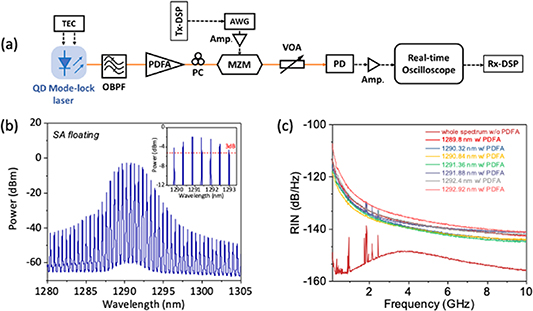
Figure 4. (a) PAM-4 data transmission setup, including DSP, digital signal processing; AWG, arbitrary waveform generator; MZM, Mach–Zehnder modulator; OBPF, optical band pass filter; PC, polarisation controller; VOA, variable optical attenuator; PD, photodetector. (b) Optical combs under bias condition of  = 66 mA at room-temperature. (c) RIN spectrum of the whole spectrum and the filtered 7 tones within the 3 dB bandwidth in (b).
Download figure:
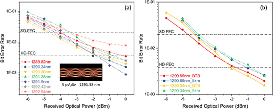
Standard image High-resolution imageThe uniformity of the different channels is compared by measuring the 64 Gbaud PAM-4 (128 Gbit s−1) signal transmission in both B2B and 5 km SSMF. Figure 5(a) shows the calculated transmission results versus received optical power for seven carriers under the same bias condition as in figure 4(c) while the figure 5(b) presents the 5 km standard single mode fibre (SSMF) transmission performance for two chosen tones (1290.34 and 1290.86 nm). In both figures, the HD-FEC stands for 7% overhead hard decision and the SD-FEC represents the 20% overhead soft decision. As indicated, the BER curves, aside from the one located near the edge at 1292.24 nm, show similar behaviours with the values of BER well-underneath the HD-FEC threshold at 0 dBm received power. The receiver sensitivity of this QD MLL (at BER = 3.8 × 10⁻³) equals 1.6 dBm and the power penalties for two measured tones are about 1 dB. Meanwhile, the similar slope efficiency and the overlapped points shown in the graph indicate a reasonable consistency of performance between separate channels. The 64 Gbaud PAM-4 electrical eye diagram for channel 1291.38 nm is measured by a digital communication analyser (DCA) (Keysight 86100D DCA-X) and presented in the inset of figure 5(a). The clearly opened eyes suggest a good signal quality in the digital domain.
Figure 5. BER performance of 64 Gbaud PAM-4 signal with different comb lines for (a) B2B transmission and (b) 5 km SSMF transmission.
Download figure:
Standard image High-resolution image
4. Conclusions
We have developed a wide-spaced OFC source generated by an unbiased passive two-section InAs QD MLL with an ultrahigh fundamental repetition rate. Thanks to the high dot density, good QDs uniformity, as well as the special design of the laser structure, ML is observed with only the current source in a laser cavity as short as 405  m (corresponding to a mode spacing of 94 GHz between adjacent tones). The nearly-transform-limited pulses can be detected throughout the test range. Meanwhile, the QD-MLL shows excellent intensity noise performance with a typical integrated average RIN value less than −134 dB Hz−1 over the frequency range from 100 MHz to 10 GHz. Seven selected wavelengths are utilised as optical carriers to successfully demonstrate a system-level 64 Gbaud PAM-4 (128 Gbit s−1) transmission experiment. The measured results suggest that our QD-MLL is a compelling candidate as a small footprint, low power consumption, easy operation, and cost-efficient on-chip DWDM light source in the future high-speed PICs.
Acknowledgments
The authors would like to acknowledge Dr Mu-Chieh Lo, Dr Zichuan Zhou and Dr Zhixin Liu from University College London for the helpful discussions, and Dr Wei Li from Beijing University of Technology for performing TEM characterisation. S C acknowledges the Royal Academy of Engineering for funding his Research Fellowship. S P acknowledges the China Scholarship Council for funding her study.
Data availability statement
The data that support the findings of this study are available upon reasonable request from the authors.
Funding
UK Engineering and Physical Sciences Research Council (EP/T01394X/1 and EP/P006973/1); Royal Academy of Engineering (RF201617/16/28); European Project H2020-ICT-PICTURE (780930).