
Abstract
We present an experimental set-up for the controlled application of strain gradients by mechanical piezoactuation on 3D crystalline microcantilevers that were fabricated by focused ion beam machining. A simple sample design tailored for transport characterization under strain at cryogenic temperatures is proposed. The topological semi-metal Cd3As2 serves as a test bed for the method, and we report extreme strain gradients of up to  m−1 at a surface strain value of
  at 4 K. Interestingly, the unchanged quantum transport of the cantilever suggests that the bending cycle does not induce defects via plastic deformation. This approach is a first step towards realizing transport phenomena based on structural gradients, such as artificial gauge fields in topological materials.
Export citation and abstract BibTeX RIS

Original content from this work may be used under the terms of the Creative Commons Attribution 4.0 license. Any further distribution of this work must maintain attribution to the author(s) and the title of the work, journal citation and DOI.
1. Introduction
The interplay between lattice and electronic degrees of freedom is essential for the understanding of solids. Unidirectional strain has proven to be a powerful parameter to tune quantum states in many classes of materials, such as electronic nematics [1], unconventional superconductors [2], or complex magnets [3]. Similarly, if (quasi-)degenerate ground states (e.g. different crystal structures) exist, the rather weak perturbation of the elastic deformation can push the system into a different topological ground state [4]. Yet uniaxial strain can tune topological semi-metals (TSMs) in non-linear ways. For example, strain has been shown to prompt a transition to a fully gapped quantum spin Hall insulator [5], induce topologically non-trivial surface states [6] or to change the sign of a Dirac band gap [7].
Given the commonly subtle influence of strain on the electronic structure of solids, which is often treated as a small perturbation, it is not surprising that strain gradients are typically ignored in the description of metals—with the notable exception of the lattice mismatch strain in epitaxial thin films. Yet as we approach the micro- and nano-scale, significant strain can be found even in 3D crystals [8]. Due to the small dimensions, the magnitude of strain gradients can become significant. Most prominently, strong strain gradients have been linked to unique phenomena in Dirac materials. For example, flat Landau levels with a gap compatible with the emergence of an effective magnetic field of the order of hundreds of Tesla have been observed in graphene [9] and artificial 2D Dirac systems [10]. The strength of this effective magnetic field is determined by different intrinsic degrees of freedom, which are able to produce drastic band structure effects similar to those caused by external magnetic fields, while still preserving time-reversal symmetry [11].
In Weyl semi-metals (WSMs), strain gradients can couple to the momentum space location of the Weyl points and produce effective magnetic and electric fields that are sensitive to the chiral charge of the nodes. This coupling is expected to be more robust and rich in phenomenology than that of the 2D case. Since Weyl points are topologically stable and not protected by crystalline symmetries, strain gradients of various types are expected to move them rather than gap them. In addition, intrinsic fields can either break or preserve time reversal or inversion symmetry depending on the particular setting. Like extrinsic fields, intrinsic magnetic fields are expected to result in dispersing chiral Landau levels in the vicinity of the nodes, that in turn will derive local equilibrium persistent currents as well as effects akin to the chiral anomaly [12, 13].
Strain gradients in a WSM can be modelled by introducing a spatially dependent node position  that can couple to the Weyl nodes of different chirality with an opposite sign [13–18]. The node position formally takes the role of a vector potential of the pseudo-magnetic field via
  , which yields non-zero values in the presence of strain gradients. Such an intrinsic field can act on fermions of opposite chirality with an opposite sign. In 3D materials, pseudo-fields have been realized using acoustic and photonic metamaterials where pressure and light waves exhibit a linear dispersion relation that mimics that of a WSM [19, 20]. Moreover, cold atom systems have been successful in mimicking and controlling effective gauge fields [21, 22] and there are proposals for synthetic realizations of axial gauge fields analogous to B5 [23]. Despite these promising prospects, no such effects have been yet realised in 3D TSMs. Yet the realization of pseudo-magnetic fields would be highly interesting from both fundamental and practical considerations. Their magnitude is a property of the band structure, and hence the effective field values may easily exceed the highest available real magnetic fields—allowing the study of topological matter deep in the ultra-quantum limit. Without the need for real magnetic fields, this also opens the possibility to access strongly Landau-quantized topological materials in applications.
A possible pathway towards experimentally detect pseudo-fields and strain-related effects in TSMs is based on the strain-dependence of Weyl orbit oscillations. These coherent orbits in finite-size TSMs are composed of bulk sections from the chiral Landau level combined with the Fermi arc sections on the opposite surfaces of the material [24]. Signatures of coherent Weyl orbits have been observed in quantum oscillation measurements in microstructured samples [25] and nanoscopic plates [26] with a thickness below the electronic transport mean free path. As the Fermi arcs terminate at the surface projection of the bulk nodes, the Weyl orbits are naturally highly sensitive to changes in the node by strain and are predicted to change their oscillation period in the presence of pseudo-magnetic fields [17]. Furthermore, the Weyl orbit process has been argued to be responsible for a 3D version of the quantum Hall effect recently reported in nanoribbons [27].
Full control over the strain landscape in the material is at the core of controlling effective fields. Most approaches to generate strain at the micro- and nanoscale focus on 2D materials and thin films [28], which include for example biaxial strain from lattice mismatch [29], the use of flexible substrates such as polyimide films [30] and nanoindentation by atomic force microscopy tips [31]. In the case of graphene, complex strain fields acting on both sublattices independently have been proposed to induce constant effective magnetic fields [32]. Experimentally, very interesting approaches to generate high effective magnetic fields have been invented based on transferring graphene to nanopillars arrays [33] and precisely shaped nano-dots [34] and anti-dots [35], thus subjecting the graphene membrane to a nonuniform distribution of strain. However, the lack of a controllable method to introduce such strain distribution has hindered progress in this area.
3D materials can provide a platform to more easily generate and control strain gradients and their associated effective magnetic fields in TSMs. Here we present the first step on this path, and showcase an apparatus able to bend micromachined cantilevers to extreme curvature radii while simultaneously measuring the quantum transport in them. While the current progress does not yet allow an unambiguous identification of pseudo-fields, the here presented methodology will enable this in the future. Indeed, our results conclusively demonstrate that nearly constant strain gradients exceeding  m−1 can be achieved at a surface strain value of
  . The transport behaviour and quantum oscillation spectrum of the samples before and after maximum bending remains unchanged, suggesting that the bending procedure is done elastically, without irreversible structural consequences to the material itself.
2. Fabrication of cantilevers for bending experiments
The main idea presented here is based on bending microscopic, free-standing crystalline cantilevers using a macroscopic, mechanical piezo-driven positioner, while simultaneously measuring the resistance of specifically machined flexures that focus and shape the bending strain (figure 1). The Dirac semi-metal Cd3As2 is ideally suited due to its simple electronic structure consisting of two Dirac points and the cleanliness of available crystals. The crystal size, however, is small ( 1 mm), which precludes traditional lithography-based cantilever fabrication. Instead, Focused-Ion-Beam (FIB) machining is used to carve the cantilevers from these crystals [36]. In this section we present the flow process for the cantilever design and fabrication, while the details of the bending apparatus are given in the following section.

Figure 1. Sample design for transport measurements under large strain gradients. (a) Schematic diagram of a bending cantilever (purple) with electrical contacts that are Pt welded (blue) to a substrate with a Au layer on top (yellow). (b) Simulated potential distribution and current density streamlines. (c) Simulated strain εxx
distribution for a maximum vertical displacement of  m of the free end of the cantilever. (d) Scanning electron microscopy image of a FIB-fabricated Cd3As2 cantilever welded at the edge of a sapphire substrate.
Download figure:
Standard image High-resolution imageOur cantilever design starts with a large scale slab of Cd3As2 whose shortest dimension points along the desired direction of strain gradient. In order to avoid bending the electrical contacts and the engagement point of the bending apparatus, a segment of the slab is thinned down, dividing it into three sections along its long axis. The first one is composed of four thick platinum electrical contacts that are firmly connected to the substrate. They are followed by three thin flexures, the two outermost of which act as current and voltage leads, while the central bar is the active part being measured. Finally, a long and thick free end of the cantilever is used to dock the positioner.
A finite elements simulation of the electrical situation for this sample design is presented in figure 1(b), showing the distribution of the electrical potential and the current density streamlines for Cd3As2 crystalline bars. The current density is approximately uniform in the central flexure and the thick part of the cantilever can be approximated as an equipotential given its much larger size. The thin flexures are important for two main reasons: (i) the flexures concentrate the strain, minimizing the radius of curvature and maximizing the strain gradient. This is supported by finite element simulations of the cantilever with a vertical displacement applied at the free end (figure 1(c)). As expected for a simple beam under bending strain, in these simulations the strain εxx changes from its minimum (negative) value at the top to its maximum (positive) value at the bottom surface, crossing the neutral plane in the middle of the flexures; (ii) the central active bar thickness must not exceed the mean free path of the material to maintain coherence of the Weyl orbits (which is about 1 µm in these Cd3As2 crystals) [25]. Leaving the remaining cantilever thicker than this dimension ensures that the oscillatory signal from Weyl orbits only originates from the thin central flexure, whose resistance is the dominant term in the electrical signal. Figure 1(d) shows a false-colour scanning electron microscopy image of a finished Cd3As2 cantilever.
Next, we turn to the main stages of the FIB fabrication process flow (figure 2). The devices were machined using both Ga-ions and Xe-ions beams. From a Cd3As2 bulk crystal, whose crystallographic directions had been determined by x-ray diffraction, rectangular bars or lamellae of  m3 dimensions were cut along the desired directions (figure 2(a)). Throughout the fabrication, a dwell time of 1
 s was used. The coarse cuts were performed with beam currents of 60 nA at 30 kV. Using a micromanipulator, this lamella was transferred in situ to a Cu holder commonly used in transmission electron microscopy (grid), where it was thinned down to its final dimension (including the thinnest region where the flexures were located) and carefully polished to guarantee smooth and parallel surfaces (figure 2(b)). This was achieved by using smaller currents and directing the beam to pattern at grazing angles with respect to the surface of the lamella. For example, the lamella faces in figure 2(c) were polished using 4 nA while the thinning down of the flexures was done using 300 pA. The final pattern was structured top-down at a current of 1 nA (figure 2(c)). This minimizes the redeposition of sputtered material and sharp, well defined features can be obtained easily. This structural precision is critical as the Weyl orbit phase depends on the thickness of the traversed bulk [24]. Finally, the structured cantilever was mounted on the edge of a sapphire chip by ion-assisted chemical vapour deposition of Pt, forming both electric contacts to predefined Au leads on the sapphire chip and solid mechanical connections (figure 2(d)).
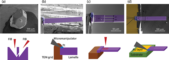
Figure 2. Main steps in the fabrication of cantilevers. (a) Oriented crystal from which rectangular lamellae are cut along the desired crystallographic directions. (b) The lamella (purple) is transferred to a grid (brown) where it is then polished. (c) The microstructuring is done while the lamella is attached to the grid. (d) The patterned cantilever is welded with platinum (blue) to the edge of a sapphire chip where gold contacts (yellow) are delineated with the FIB.
Download figure:
Standard image High-resolution image3. Bending apparatus
In our apparatus the fabricated cantilevers are bent using a piezo-actuated pusher (figure 3). The mechanical motion is provided by an Attocube linear nanopositioner equipped with a potentiometric readout of the platform position with a resolution close to 300 nm at cryogenic temperatures (model ANPz51). The measurements are performed in a Quantum Design physical properties measurement system (PPMS) coupled to a multi-channel Lock-in amplifier (Synktek). An AC excitation current of 50 µA at 177.77 Hz is applied to measure the flexure resistance in a four-probe geometry. The design permits the positioning of the sample far away from the pusher when piezoactuation is not engaged. It includes two pieces (see figure 3(b)): an external cage to fix the nanopositioner to the puck (grey); and a mobile top part fixed to the nanopositioner that is to serve as the 'pushing' part (red). Electrical contact pads can be conveniently glued down on the top of the external case. Key to obtaining a reliable bending motion of the cantilever is a properly designed mating piece on the pusher side. A silicon chip with a sharp FIB carved edge of around 7 µm width is manually placed under the cantilever. In this way, a flat, well defined contact line can be achieved.
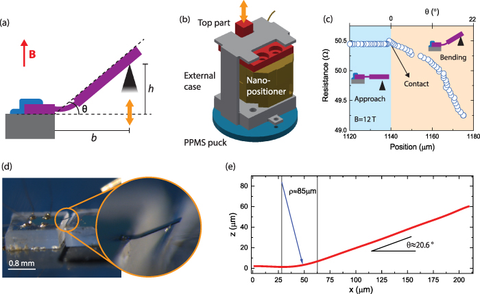
Figure 3. Bending apparatus. (a) Schematic diagram of the cantilever during bending. (b) Schematic diagram of the fabricated sample holder used to mount the nanopositioner on the PPMS puck. (c) Approach and bending cycle as monitored via the change in the cantilever MR. (d) Optical image of a fabricated cantilever under bending. (e) Experimental profile of a bent cantilever, obtained from an optical image, showing the measured radius of curvature and corresponding bending angle.
Download figure:
Standard image High-resolution imageTo avoid any unknown strains from differential thermal conduction, the design purposely avoids a solid connection between the cantilever and the mobile pusher during temperature sweeps. Instead, the pusher is cooled down at a safe distance ( m) below the cantilever. Once at base temperature, the pusher is slowly moved upwards to mechanically engage with the cantilever. A critical point is to detect the moment of contact between the pusher and the cantilever. This can be done by observing a change in the resistance of the sample at constant magnetic field. Given the extreme magnetoresistance (MR) typical of TSM [37], a strong response of the resistance even to small angle changes between the field and the cantilever is expected. Indeed, a sharp anomaly signals the touching point followed by a strong decrease of the MR with increasing bending in the Cd3As2 cantilevers (figure 3(c)). In combination with the displacement readout of the piezo drive, this allows to in situ calibrate the relative distance between cantilever and pusher.
Yet the mechanical state of the cantilever cannot be directly observed in the cryostat. Hence we rely on finite element models and optical microscopy images at 300 K of bent cantilevers to investigate the degree and homogeneity of the achieved bend. As can be seen in figure 3(d), during the bending process, the thicker free end of the cantilever shows no appreciable signs of deformation nor twisting, while the flexures concentrate the strain and exhibit a well-defined radius of curvature. This mechanical state is consistent with the one obtained in our finite elements simulations (figure 1(c)).
The bending angle θ is approximated by solving a numerical equation: tan , where h is the nanopositioner's height from the touching point, t is the thickness of the free end of the cantilever and b is the distance from the edge of the sapphire chip to the pushing part (figure 3(a)). One may approximate the mechanical situation using the simple relation from beam theory under bending strain:
  , where ρ is the radius of curvature and d is the length of the sample's central flexure [38]. This leads to a radius of curvature of
  m and a bending angle of
  for the maximum nanopositioner's height used,
  m. These values are in good agreement with a direct analysis of the optical image of a bent cantilever with a similar h (figure 3(e)), from which we obtain a bending angle of
  and a radius of curvature of
  m.
m.
Using the expression for the strain on a thin beam  , one estimates the value of the strain gradient as
 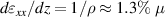 m−1. The value of the the surface strain is then calculated to be
  , which compares well with the value obtained in the finite element simulations (figure 1(c)). These simulations also suggest a rather uniform strain distribution on the flexures surfaces.
It is important to check for possible plastic deformation of the cantilever, especially given the substantial bending angles in the experiment. A first indication is given by a comparison of the MR at zero bending before and after bending to a large angle,  (figure 4(a)). Indeed, the curves overlap both in the low-field region, indicating an unchanged residual resistivity, as well as in the high-field region, supporting an unchanged value of
  (ωc
: cyclotron frequency, τ: quasiparticle lifetime). This strongly suggests an unchanged defect landscape and, hence, an unchanged τ. The presence of quantum oscillations further provides insights into the quantum transport (figure 4(b)). The oscillations are quantitatively analyzed using a fast Fourier transform (FFT) in the field range from 5 to 11 T, after subtracting a sixth-order polynomial background to remove the non-oscillatory part of the MR. The spectrum reveals the presence of two frequencies: one at
(ωc
: cyclotron frequency, τ: quasiparticle lifetime). This strongly suggests an unchanged defect landscape and, hence, an unchanged τ. The presence of quantum oscillations further provides insights into the quantum transport (figure 4(b)). The oscillations are quantitatively analyzed using a fast Fourier transform (FFT) in the field range from 5 to 11 T, after subtracting a sixth-order polynomial background to remove the non-oscillatory part of the MR. The spectrum reveals the presence of two frequencies: one at  T is consistent with previous reports corresponding to the bulk Fermi surface. The second frequency
  T agrees well with those reported for the Weyl orbit [25, 26]. No resolvable change in FBulk
nor FWeyl
is observed after bending, suggesting that no effects like increase of quantum scattering time nor remnant deformation of the Fermi surface are produced by the application of the strain gradients. We note that a subtle difference in amplitude is compatible with differences in the subtracted polynomial background. These signatures together paint a consistent picture of elastic bending without plastic deformation.
T agrees well with those reported for the Weyl orbit [25, 26]. No resolvable change in FBulk
nor FWeyl
is observed after bending, suggesting that no effects like increase of quantum scattering time nor remnant deformation of the Fermi surface are produced by the application of the strain gradients. We note that a subtle difference in amplitude is compatible with differences in the subtracted polynomial background. These signatures together paint a consistent picture of elastic bending without plastic deformation.
Figure 4. Quantum oscillations before and after maximum bending. (a) Resistance vs magnetic field at 4 K and (b) the corresponding FFT spectrum after background subtraction. The inset in (a) shows the ratio between the MR after and before maximum bending. The magnetic field direction is the same as the one depicted in figure 3(a).
Download figure:
Standard image High-resolution image
Under strong bending, the Weyl oscillation shifts to higher frequencies at reduced amplitude, while the bulk remains unchanged. It is intriguing to note that the direction of a frequency increase is compatible theoretical predictions of pseudo-field effects in Cd3As2 [11]. While tantalizing, further studies are required to explore additional effects that occur under these extreme bending strains, such as the relative change in the magnetic field direction with respect to the sample which also leads to amplitude modulation and frequency variation of the Weyl orbits [25]. Current theoretical models assume weak strain gradients, assuming that the overall shape of the strained objects remains unchanged. Our results clearly call for further theoretical studies of quantum states in topological semi-metals under strong strain gradients that significantly distort the shape of the physical crystal.
4. Conclusion
We have presented a set-up for the controlled application of large strain gradients on crystalline FIB-microstructured cantilevers of 3D TSM that have been designed for transport measurements down to cryogenic temperatures. Despite the large deformation, transport evidences this to be well within the elastic limit. This experimental methodology and apparatus presents a first, crucial step towards the creation of pseudo-magnetic fields in 3D TSMs. Yet the versatility of the fabrication technique allows to apply this approach to a large variety of crystalline materials beyond the direct scope of effective magnetic fields. For example, strain gradients may tune further topological phenomena such as topological phase transitions and high order topological phases [39–43]. Furthermore, if strain gradients can produce additional effects beyond changing the position of the Weyl points, such as creating tilt gradients of the Weyl cones, it is possible that additional effects such as analogs of event horizons or a realization of the mixed-axial gravitational anomaly can be accessed [44, 45]. With strong strain gradient fields now controllably available in 3D solids, new ideas to create and control distorted quantum materials can be realized in the future.
Data availability statement
The data that support the findings of this study are openly available at the following URL/DOI: https://doi.org/10.5281/zenodo.5117954.
Acknowledgments
We are grateful for stimulating discussions with Dmitry I Pikulin. This work was funded by the European Research Council (ERC) under the European Union's Horizon 2020 research and innovation programme (MiTopMat—Grant Agreement No. 715730). A G G acknowledges financial support from the European Union Horizon 2020 research and innovation program under Grant Agreement No. 829044 (SCHINES). R I is supported by the Israel Science Foundation Grant No. 1790/18.
4. Author contributions
P J W M, J D, C P, D S, A G G and R I conceived the study. J G A synthesized the single crystals. X H and C P performed the x-ray analysis of the crystals. J D and A E designed the bending apparatus. J D, X H and C P microstructured the crystals. J D and C P performed the measurements and data analysis. All authors contributed to writing the manuscript.