

Abstract
Thin metallic buffer layers are commonly used between semiconductor substrates and noble metal films or nanostructures. We propose an extended two-temperature heat transfer model that can be used to investigate the heat flow in multilayer antennas and includes metallic layers, a dielectric substrate, and their respective interfaces. It is demonstrated how the heat flow dynamics in a layered material, excited by short laser pulses, can be controlled by the thermal properties of the buffer layer. A large buffer layer electron-phonon coupling was found to induce a non-intuitive reverse internal heat flow in the layered material and transient energy retention on time scales of a few tens of picoseconds, while the buffer layer-substrate Kapitza conductance was found to be the limiting parameter for the heat dissipation on nanosecond time scales.
Export citation and abstract BibTeX RIS
1. Introduction
A growing number of techniques utilizing high power short laser pulses (<10 ps) have been developed during the last decades for applications ranging from surface treatment and laser patterning to high power electronics [1–5]. In nanostructured composite materials such as metallic films and multilayers, short laser pulses can be used to measure diverse mechanical, thermal, and optical properties [6–12]. Short laser pulses are frequently used to study properties of light stimulated active metamaterials and metasurfaces (MMs & MSs), with operating frequencies from the terahertz to the optical range [8, 13–15].
Without control over the heating mechanism and energy dissipation, absorbed laser light may cause thermal distortions and even damage, limiting the lifetime of devices. Therefore, understanding the heat transport mechanisms has become increasingly important [16]. Pinpointing the relation between geometry, material choice, interfaces, and heat flow is required for reliable device design [17, 18]. Examples thereof can be found in mirror design for high power infrared (IR) systems, heat dissipation in electronic circuits, heat recycling for energy harvesting, thermal control in nano systems, active MMs, and the field of thermoplasmonics [5, 14, 19–23].
Since the appearance of Fourier's diffusion law in the 19th century, diverse models have been developed to describe the heat flow between solids [16, 24–26]. The dawn of the electronic era initiated a strong reduction of the sizes and reaction time of components in (opto)electronic devices. One-temperature models cannot accurately describe the heat flow dynamics of materials at ultra-short times, i.e. after excitation by picosecond long intense laser pulses, because the electron and lattice subsystem are not in equilibrium. The electrons heat up much faster than the atomic lattice. Later new models appeared that consider energy transfer between subsystems and more accurately describe the heat flow dynamics, particularly in situations where the excitation pulse is comparable to or shorter than the time required for the electron and lattice subsystems to reach thermal equilibrium. One of these models is the two-temperature model (TTM), which treats the electron and lattice subsystems separately. The TTM was introduced in 1974 by Anisimov et al while studying the interaction between metals and picosecond laser pulses [24]. Since then, this model has experienced considerable development and was used in diverse experimental and theoretical studies [25, 26].
Considering a time scale ranging from a few to a few hundreds of picoseconds, it is generally accepted that the relevant heat flow processes following plasmonic excitations by a laser pulse are electron-phonon (e-ph) coupling and heat diffusion. On this time scale, a homogeneous electron temperature is usually assumed, since electron–electron scattering is much faster, taking place on the femtosecond timescale. The electron and lattice subsystems equilibrate via the e-ph coupling interaction in a few tens of picoseconds, during which the excess thermal energy is transferred from the electron to the lattice subsystem via collisions. In metallic multilayers or in systems where an adhesion layer is present, the e-ph equilibration process may be different in each layer, thereby affecting the heat flow. Diffusion takes place in the metallic layers and substrate as described by the Fourier law. Across the different interfaces, heat flow is described by the Kapitza interface conductance [3, 16, 17, 26–29].
Previous work has dealt with the non-equilibrium heat flow between different metallic layers and interface heat conduction between metals and dielectrics [17, 30, 31]. A few papers reported on the role of the metal bilayer composition for microscopic heat generation and thermal stability under continuous laser excitation [22, 23]. Short optical, far-IR, or THz pulses have been used to study the performance of active MMs and MSs inducing electronic excitations in the substrate [8–11], stimulate metal–insulator transitions [12, 32], or change the properties of resonant structures [33]. However, the heat flow dynamics in layered metallic structures following picosecond laser excitation has so far not been studied in depth. Heat flow following picosecond laser excitation is fundamentally different from both continuous laser excitation and femtosecond laser excitation since the e-ph coupling and the heat conduction in nanofilms both take place at the picosecond time scale. For a femtosecond laser pulse the lattice heating only occurs once the laser pulse has passed and the maximal electronic temperature is considerably higher; in that case phenomena like Landau damping, electron–hole pair decay through re-emission, and electron–electron induced carrier multiplication [34], must be accounted for.
Intense laser pulses can excite electromagnetic resonances of MMs or MSs. Those resonances are the most important characteristic of MMs and enable their different exotic optical properties [35–37]. While the optical characteristics of MMs are determined by the design of the subwavelength resonators and their periodic arrangement, the heat flow following electromagnetic excitation does not depend on this periodicity and can be modeled by a single unit cell.
The purpose of the present work is to introduce a heat transfer model for planar periodically arranged metallic bilayer structures on a semiconductor substrate, excited by picosecond far-IR laser pulses. In particular, the thermodynamic behavior of homogeneously illuminated cut-wire (CW) antennas with a dipolar antenna resonance mode is presented. The presented model is an extension of the TTM. It is made in order to consider multiple (two in this case) metallic layers (the antenna and the adhesion layer), their interface, and the interface with a dielectric substrate. Thus, this study aims to clarify non-intuitive heat flow in metallic multilayer structures and to serve as reference for the heat flow design of (meta)materials with potential applications in high power optics, tunability/fast switching, and energy harvesting.
2. Analytical model
The modeled system consists of a periodic array of metal-bilayer CW antennas; with a metallic top layer thickness of 100 nm and a thin (5–20 nm) metallic buffer layer on a thick (>100 µm) silicon substrate. Such thin buffer layers are commonly used as adhesion layers for other metal films (like gold, silver, aluminum, and others) on semiconductors, due to the poor adhesion of those metals on silicon and silicon oxide at room temperature [38]. The heat flow model is applied in one dimension for a single CW antenna under the assumptions that: (i) the CWs are homogeneously illuminated (laser spot size is much larger than the CW dimensions) and (ii) the lateral dimensions of the CW structures are at least an order of magnitude larger than their height (d ≪ l) [29]. The commercial software CST Microwave Studio [39] was used to simulate the absorption spectrum of the periodic CW antennas (see figure 1(a)), which allows to calculate the absorbed energy per CW antenna and to determine the wavelength dependence. The periodic nature of the studied system is important for the absorption spectrum since it determines the resonance frequency and thus the amount of absorbed laser energy.

Figure 1. (a) Simulated absorption spectrum of 4 × 1 μm2 CW antenna (9 × 5 μm2 cell size). The insert in panel (a) contains a schematic view of a unit cell. (b) Schematic cross section of the studied CWs (not to scale) and the considered heat flow mechanisms; e-ph coupling (circular arrow), heat diffusion and interface heat conduction (straight arrow). The relevant parameters for the different heat flow mechanisms (g, α, and G, respectively) are also indicated.
Download figure:
Standard image High-resolution imageThe lattice is not directly heated; the heat enters the system via laser excitation of the electronic antenna dipole resonance. Hot electrons are generated and heat up the electron subsystem by electron–electron scattering taking place in the femtosecond time scale, which can be considered instantaneous if picosecond laser pulses are used. Because electrons move fast and easily cross most metal–metal interfaces, it can be assumed that the electron gas of the CW's top and buffer layer are heated simultaneously and that there is no temperature gradient in the electron system [29, 31, 40].
Heat transfer processes start already during the picosecond laser excitation [41]. We consider three heat transfer processes: e-ph coupling in the top and buffer layer, bulk heat conduction, and interface Kapitza conduction. Those heat transfer processes determine, together with the laser excitation, the entangled heat flow in the system. The precise dynamics, however, strongly depends on the values of involved parameters (layer thickness, heat capacities, coupling constants, and laser pulse duration and energy) [31, 42–44].
The time dependent temperature of the electron system (Te ) is described by [27]:
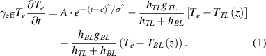
Here  (J m−3 K−2) determines the electron heat capacity (
 ). Under the assumption that a single electron gas spreads over both metallic layers,
  is a weighted average value:
  where
where  and
and  are the thickness of the top and buffer layer, respectively. The first term on the right-hand side of equation (1) concerns the absorbed power per CW and per laser pulse, assuming a Gaussian time profile with the pulse standard deviation σ and maximum intensity at time c. A is a constant regarding the average CW absorbed energy density during the laser pulse, proportional to the absorption coefficient obtained from the simulations in figure 1(a). The second and third terms on the right-hand side of equation (1) deal with the e-ph coupling in the top and buffer layer, respectively.
  and
and  (W m−3 K−1) correspond to the e-ph coupling factors in the top and buffer layers, respectively.
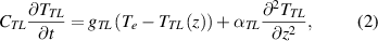
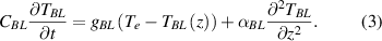
The time-dependence of the lattice temperature within the top and buffer layers,  and
and  , depends on the heat capacity of the layers (
 and
and  in J m−3 K−1), the coupling to the electron system, and thermal diffusivities (
 and
and  ) of the layers:
For temperatures around or above room temperature (∼300 K), the heat capacity of most solids can be assumed constant. The Debye model predicts that any solid will reach over 80% of its maximum heat capacity when the temperature reaches half of the Debye temperature. This temperature is lower or comparable to room temperature for the elements used in this study, pointing to limited changes of the heat capacity with a further increase of the temperature. However, a constant heat capacity would not be a good approximation at cryogenic temperatures.
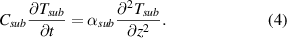
In the silicon substrate, we consider the bulk conductivity as the sole heat transfer mechanism:
At the interfaces between the top and buffer layer, as well as between the buffer layer and substrate, interface conductance takes place. This can be described by the following equation [45–47]:
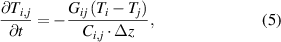
where  (W m−2 K−1) corresponds to the Kapitza conductance and the vertical step size
  relates to the material portion affected by the interface heat conduction. The indexes i and j refer to the different materials on both sides of the interface (either the top and buffer materials or the buffer layer and the silicon substrate).
Equations (1)–(5) are solved simultaneously using Robin mixed boundary conditions: Dirichlet boundary conditions at the lower end inside the substrate and the Neumann boundary condition at the top surface and at the interfaces. The time step was chosen to be 5 fs, which is small enough to analyze the heat flow dynamics on the picosecond time scale. The vertical step size  was chosen to be 1.25 nm, which is consistent with the time step since the thermal diffusion length (
 ) at t = 5 fs is in the range of 0.4–1.6 nm for the involved materials [48].
The dynamics described by the model, corresponding to equations (1)–(5), is schematically depicted in figure 1(b). As a benchmarking case we compared the outcome of our model with the maximal electron temperature that was obtained in a gold film that was heated by a 0.4 ps laser pulse [2]. The absorbed energy was matched with that of a gold film (which has a lower absorbance at 800 nm) and the buffer layer was artificially removed by using Au for the top and buffer layers and by making the interface conductance between the metal layers perfect. The maximal electron temperature of 2750 K in [2] is consistent with the 2900 K we obtained.
3. Parameter selection and ranges
The model described by equations (1)–(5) was solved for a silicon substrate supporting a metal bilayer CW antenna; each antenna is composed of a 100 nm gold top layer and a 20 nm buffer layer made of different materials. The selected laser excitation parameters correspond to a micropulse of the IR free electron laser (FELIX) at the Radboud University in Nijmegen, The Netherlands [54], which was used in our previous experimental study on the transient transmission of THz MM antennas [8]. The excitation laser pulse is 8 ps long, with a fluence of 8 J m−2, and has a Gaussian shape. Considering such a laser excitation and an absorption of 22% at a wavelength of 23 μm (see figure 1(a)), we can calculate a value of 4 × 10⁷ W m−3 for the power density amplitude in equation (1) (parameter A).
Different real and fictitious materials are considered for the buffer layer, which affects the system through variations in the different thermodynamic parameters:  ,
,  ,
,  , and
, and  . To systematically study the effect of these parameters on the heat flow dynamics, we selected a range of representative values and varied them either independently or using the parameters values of real elements. The selected parameter values are given in table 1. These values are mostly taken from real materials, but some fictitious material values are added to either fill in gaps or extend the parameter range. The Au parameter values were taken as default:
  W m−3 K−1,
  J m−3 K−2,
  = 2.49 × 10⁶ J m−3 K−1,
  = 88 × 106 W m−2 K−1. Since the top layer is made of gold as well, this implies the default corresponds to a system without a buffer layer.
Table 1. Parameter values considered for the buffer layer. These parameters are either varied independently from one another or multiple parameters, belonging to a single element, are varied simultaneously.
E-Ph coupling ( ) 1016 W m−3 K−1 ) 1016 W m−3 K−1
| Buffer layer electron heat capacity ( ) J m−3 K−2 ) J m−3 K−2
| Lattice heat capacity ( ) 106 J m−3 K−1 ) 106 J m−3 K−1
| Buffer layer-silicon Kapitza conductance (GBL/Si ) 106 W m−2 K−1 | |
|---|---|---|---|---|
| Default values | 3.00 (Au) [31] | 67 (Au) [29, 31] | 2.49 (Au) | 88 (Au/Si) [31] |
| Other values | 1.00 | 2.00 | ||
| 8.00 | 91 (Al) [49] | 2.36 (Ti) | 90 (Pt/Si) [17] | |
| 27.8 (Al) [50] | 193 (Cr) [7] | 2.42 (Al) | 170 (Al/Si) [51] | |
| 42.0 (Cr) [7] | 330 (Ti) [31] | 2.80 (Pt) | 178 (Ti/Si) [31] | |
| 105 (Ni) [50] | 750 (Pt) [19] | 3.20 (Cr) | 180 (Ni/Si) [52] | |
| 130 (Ti) [31] | 1065 (Ni) [53] | 3.91 (Ni) | 200 (Cr/Si) [19] |
In addition to this, the influence of the pump pulse fluence (in the 2–12 J m−2 fluence range), the excitation wavelength, and the buffer layer thickness (in the 5–20 nm range) were considered. Since the influence of those parameters was limited to magnitude changes but not to a difference in the heat dynamics, they are not discussed further. Finally, the laser pulse duration is also contemplated in this work to study the limitations of the buffer layer effect on the dynamics.
4. Results and discussion
Figure 2 shows the evolution of the different subsystems' temperatures (electrons, top layer lattice, buffer layer lattice, and silicon substrate) for a high and a low considered  ,
,  and
and  value, as well as for different laser pulse durations. The silicon temperature is probed at 100 nm below the silicon/buffer-layer interface, the top layer temperature is probed at the surface, and that of the thin buffer layer near the interface with the substrate. The overall heat flow dynamics is in line with the general expectations: the electron subsystem is quickly heated up during the exposure to the laser pulse; after which the heat flows toward the top and buffer layer lattices (on times scales of a few to a few tens of ps); finally, the silicon substrate acts as a heat sink. The maximal temperatures reached in the different subsystems and the exact moment this occurs depend on the precise buffer layer parameter values as well as on the laser pulse duration.

Figure 2. Temperature evolution of the different subsystems: electrons in the metal bilayer, top layer lattice, buffer layer lattice, and silicon at 100 nm below the silicon-buffer layer interface. (a) Comparison of  = 67 and 1065 J m−3 K−2 (
 =
=
 and
and  =
=  ). (b) Comparison of
  = 2.36 × 10⁶ and 3.91 × 10⁶ J m−3 K−1 (
 =
=  and
and  =
=  ). In this panel the electron temperature for both cases is almost identical and the curves superimpose. (c) Comparison between
  = 3 × 10¹⁶ and 130 ·1016 J m−3 K−1 (
 =
=  and
and  =
=  ). (d) Shows a system identical to the one in (c) excited by a laser pulse of the same energy but a duration of 80 ps.
Download figure:
Standard image High-resolution imageFigure 2(a) shows that the effective electron heat capacity mainly influences the electron subsystem. A higher  implies a lower maximal
  , which is reached at a slightly later moment, as well as a considerably longer cooling time. The longer retention of the energy in the electron subsystem goes along with an additional ∼15 ps required for the lattice temperature to reach its maximum value. Since the electron-lattice energy transfer scales with electron-lattice temperature difference (see equations (2) and (3)), the heat flow from the electrons to the lattice will be slower (even if the e-ph coupling rate is the same) if the temperature difference is smaller. Therefore, both the electron subsystem and the lattice reach their maximal temperature at a slightly later moment.
The effect of the buffer-layer heat capacity is presented in figure 2(b). A higher  evidently implies a lower maximal buffer-layer temperature and a different temporal evolution for
  . The influence of the other subsystems (electrons, top layer, silicon) is very limited since the buffer layer is relatively thin (thickness of 20 nm compared to a 100 nm top layer). The electron temperature is not influenced since the buffer layer heat capacity is only relevant in a later phase of the heating process. Hence, a variation of the buffer-layer heat capacity does not significantly alter the system's thermal response beyond a several tens of ps delay for
  to reach its maximum value.
The buffer layer e-ph coupling factor,  , has a stronger effect on the heat flow dynamics than γeff and
  . As can be seen in figure 2(c), a high
  results in a strong reduction of the maximal electronic and top layer temperatures along with a strongly increased buffer-layer temperature during the first 10 ps. Most interestingly, a high buffer layer e-ph coupling constant prompts the emergence of a counterintuitive heat flow. A large fraction of the energy absorbed by the electron subsystem is quickly directed and temporarily accumulated in the buffer layer. After a few tens of ps the top and buffer layers reach their equilibrium temperature. This implies a heat flow from the buffer to the top layer, as opposed to the intuitively expected sequential top layer, buffer layer, silicon substrate heat flow. The variation of
  proves to be an efficient way to tune the thermal response of the sample and transiently store significant fractions of the absorbed energy in the (thin) buffer layer.
Figure 2(d) shows the thermal dynamics for the same sample as in figure 2(c), excited by a laser pulse of the same energy but a longer duration of 80 ps, i.e. a power that is an order of magnitude lower. The presence of the buffer layer becomes notoriously less significant and lower electron temperatures are reached because the e-ph equilibration time becomes comparable to the pulse duration. For even longer pulse duration, the TTM eventually becomes unnecessary, as the electron and lattice system remain in (or near) equilibrium. These results are further illustrated in figure 3, where the temperature variation is presented from a cross section perspective for different values of the buffer layer e-ph coupling constant and the laser pulse duration.
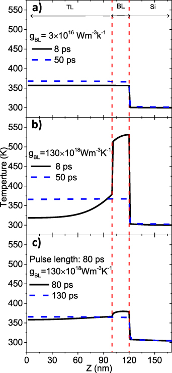
Figure 3. Temperature depth profile of the sample at the end of the laser pulse and at a later moment. Results obtained for (a)  =
=
 = 3 × 10¹⁶ J m−3 K−1, 8 ps pulse duration at t = 8 and 50 ps, (b)
  =
=
 = 130 × 1016 J m−3 K−1, 8 ps pulse at t = 8 and 50 ps, (c)
  =
=
 = 130 × 1016 Jm−3 K−1, 80 ps pulse at t = 80 and 130 ps.
Download figure:
Standard image High-resolution imageRegardless of the strength of the e-ph coupling constant and the pulse duration, the effects are short-lived. The temperature distribution inside the metal bilayer is homogeneous at 50 ps after the laser pulse. This implies that controlling the heat flow dynamics in the metallic bilayer antenna is possible, but only for short laser pulses (≲100 ps) and only during the first few tens of picoseconds after the excitation has passed. During these first few tens of ps, for the case of short pulses and high gBL , a big thermal gradient is observed at both interfaces. This pronounced gradient can signal the presence of interface stress, which potentially damages the heated structures. Our model allows to identify such potential issue prior to device fabrication.
To obtain a more quantitative understanding, we analyzed the maximal temperatures and stored energy fraction in the different subsystems as a function of the buffer layer thermodynamic parameters and excitation duration (see figure 4). Also, a combined variation of parameters, corresponding to a selected set of real metals, was studied. We defined the energy fraction as the fraction of the absorbed energy (from the laser pulse) stored in the different subsystems (electrons, buffer layer lattice, top layer lattice, substrate). They are calculated as the energy contained in a given subsystem minus the initial energy (before laser excitation), divided by the total absorbed energy.

Figure 4. (a)–(c) Maximum reached temperature and (d)–(f) maximum energy fraction for the electron and the buffer layer lattice subsystems. (a) and (d) present the dependence on the effective electron heat capacity (with  =
=  = 2.49 × 10⁶ J m−3 K−1 and
  =
=  = 2.95 × 10¹⁶ W m−3 K−1). (b) and (e) show the dependence on the buffer layer heat capacity (with
  =
=  = 67 J m−3 K−2 and
  =
=  = 2.95 × 10¹⁶ W m−3 K−1). Panels (c) and (f) illustrate the dependence on the buffer layer e-ph coupling coefficient (with
  =
=
 = 2.49 × 10⁶ J m−3 K−1 and
  =
=  = 67 J m−3 K−2). In addition to the systematic variations of a single parameter, while keeping the other parameters fixed at the Au reference values, data points for real buffer layer materials are added as filled red stars.
Download figure:
Standard image High-resolution imageFigures 4(a) and (d) show the effect of the electron heat capacity on the maximal temperature and the maximal energy fraction stored in the electron subsystem. The temporal maximum energy fraction stored in this subsystem reaches 50% for the highest considered effective heat capacity. Since all laser energy is initially absorbed via the electrons, this value is remarkably low, implying that e-ph coupling is already significant during the laser excitation (i.e. the first 8 ps). The electron gas retains the energy only for a short period of time. A similar observation can be made for the buffer layer system when  is varied (figures 4(b) and (e)), the increase of
  in the studied parameter range induces a linearly increasing accumulation of energy in the buffer layer.
The effects of the variation of the buffer layer e-ph coupling coefficient are shown in figures 4(c) and (f).  has a strong influence on both the maximum reached temperature and the energy stored in the buffer layer, as was demonstrated in figures 2 and 3. Although a high
  keeps the top layer and electron subsystems' temperature low, protecting the top layer from thermal damage, it can lead to a hot buffer layer. This can be detrimental for the system integrity in extreme cases due to the generation of a high thermally induced stress [43, 44]. The filled star symbols in figures 4(c) and (f) represent the values obtained when using real elements for the buffer layer (combined variation of
  ,
,  , and
, and  as given in table 1), allowing to observe how specific combinations of parameter values affects the maximal temperature and stored energy fractions.
An increase of either  or
or  lowers the maximum buffer layer and electron temperatures, while increasing the maximal retained energy. In contrast, a high
  facilitates an energy flow from the electron system toward the buffer layer lattice, increasing both its temperature as well as the maximum retained energy fraction. For the case of real materials (represented by the filled red stars), multiple parameters are varied simultaneously, which is reflected in a non-monotonic increase in the maximal buffer layer energy/temperature values with
  . This highlights the importance of the material selection when constructing a system subject to extreme conditions, like the exposure to short laser pulses.
The last parameter influencing heat transport is the Kapitza conductance. This parameter plays a role in the two interfaces present in the system: the buffer layer-substrate (metal-dielectric) and the top-buffer layer (metal–metal) interface. The TL–BL interface conduction has a minimal influence on the heat flow process because the metal-metal Kapitza conductance is much larger than the different  values. The GTL/BL
value was set at a representative value of 5 × 10⁹ W m−2 K−1 for all metal combinations in this work [19, 29, 55]. Given its limited influence, the metal–metal interface is not further discussed, and we concentrate on the role of the metal-dielectric interface conductance.
values. The GTL/BL
value was set at a representative value of 5 × 10⁹ W m−2 K−1 for all metal combinations in this work [19, 29, 55]. Given its limited influence, the metal–metal interface is not further discussed, and we concentrate on the role of the metal-dielectric interface conductance.
Naturally, the higher the interface conductance the faster the heat will diffuse toward the substrate. From equation (5) and the earlier results, one can deduce that  and
and  have an influence on the heat transfer rate toward the substrate, since these parameters influence the buffer layer temperature and thus the temperature gradient over the metal-dielectric interface. A series of calculations with different values of the Kapitza conductance, in combination with high
  and
and  , was performed. The obtained results are shown in figure 5.

Figure 5. Evolution of the thermal energy fraction within the silicon substrate for: (a) different values of the Kapitza conductance,  ; (b) combination of a high buffer layer e-ph coupling (130 × 1016 J m−3 K−1) and heat capacity (3.91 × 10⁶ J m−3 K−1) with a constant Kapitza conductance.
Download figure:
Standard image High-resolution image
Figure 5(a) shows the strong effects that a change in the metal-dielectric Kapitza conductance has on the scale heat flow, especially at long times compared to the laser pulse duration. The reference value (red circles in figure 5(a)), for the Kapitza conductance between the metallic buffer layer and the silicon substrate was taken as  = 178 × 106 W m−2 K−1 which corresponds to a Ti/Si interface. Titanium is commonly used as an adhesion material. For several other metals on silicon the
  values are similar (see table 1).
  = 88 × 106 W m−2 K−1 (black squares in figure 5(a) corresponds to the value of the Au/Si interface. Since the Kapitza conductance depends not only on the materials that compose the interface but also on the interface quality, it is possible to control it via the growth or by surface modification techniques [3, 17, 18, 29, 51]. For this reason, we considered a fictitious high metal/Si Kapitza conductance of 500 × 106 W m−2 K−1 (blue triangles in figure 5(a)), representing the hypothetically improved contact between metal layers and silicon substrate.
The possibility to modify the heat transfer rate toward the substrate by manipulating the local temperature gradient at the silicon interface, was also explored (see figure 5(b)). This was made possible by taking advantage of  and
and  , which allow to directly influence the temperature gradient at the buffer layer/Si interface. A material with high
  will reach a lower maximal temperature, thus decreasing the heat transfer rate toward the substrate. The opposite situation is obtained when using a material with a high
  . A variation in the thermal energy diffused toward the silicon of ∼3%, at time scales of one nanosecond, can be achieved by the selection of buffer layer materials with the appropriate values of the thermodynamics parameters. By increasing the
  , a decrease in the energy dissipated toward the substrate can be induced, which, although small, could become a considerable amount of energy when dealing with high intensity and high repetition rate lasers or thin vulnerable antennas. Meanwhile, an increase in
  has little influence on the heat flow towards the substrate.
5. Conclusion
In conclusion, we used a modified version of the TTM in combination with heat diffusion and Kapitza conductance to address the temporal and spatial evolution of the thermal dynamics within a laser-excited metallic bilayer CW on a silicon substrate. A significantly different heat flow dynamics was found depending upon the buffer layer's thermodynamic parameters, which becomes less prominent with increasing laser pulse duration or lower laser power. Buffer layer materials that are commonly used to improve the gold adhesion on a dielectric substrate were found to substantially influence the heat flow dynamics.
Our results imply that even a thin buffer layer has a considerable influence on the thermodynamic properties of the system by temporarily storing a significant fraction of the absorbed laser energy. This demonstrates that by proper material selection it is possible to exert control on the heat flow dynamics and transient energy accumulation in one subsystem, in particular the electron and buffer layer lattice systems. Our model allows to explore the buffer layer material properties and parameters that are best suited to serve as protective elements and/or as heat flow modifier elements. This way it is possible to control the thermal response and stress, and thus the heat flow and the potential thermal damage of the metallic bilayers and MM antennas when exposed to intense picosecond light pulses.
Acknowledgments
This research has been funded by a joint research project between the Vietnam National Foundation for Science and Technology Development (NAFOSTED) under Grant No. FWO.103.2017.01 and the Research Foundation Flanders (FWO) under Grant No. G0E62.18N. This work is also supported by the KU Leuven Research Council (BOF).
Data availability statement
The data that support the findings of this study are available upon reasonable request from the authors.