
Abstract
Plasmonic modes in metal structures are of great interest for optical applications. While metals such as Au and Ag are highly suitable for such applications at visible wavelengths, their high Drude losses limit their usefulness at mid-infrared wavelengths. Highly n-doped Ge1−ySny alloys are interesting possible alternative materials for plasmonic applications in this wavelength range. Here, we investigate the use of highly n-doped Ge1−ySny films grown directly on Si by molecular beam epitaxy with varying Sn-content from 0% up to 7.6% for plasmonic grating structures. We compare plasma wavelengths and relaxation times obtained from electrical and optical characterization. While theoretical considerations indicate that the decreasing effective mass with increasing Sn content in Ge1−ySny films could improve performance for plasmonic applications, our optical characterization results show that the utilization of Ge1−ySny films grown directly on Si is only beneficial if material quality can be improved.
Export citation and abstract BibTeX RIS

Original content from this work may be used under the terms of the Creative Commons Attribution 4.0 license. Any further distribution of this work must maintain attribution to the author(s) and the title of the work, journal citation and DOI.
1. Introduction
Plasmonic antennas can be utilized to enhance light–matter interaction, with applications ranging from sensing [1, 2] to enhancing [3] or enabling [4] optoelectronic device operation. For mid-infrared (mid-IR) plasmonic applications, heavily doped semiconductors such as Ge and Ge1−y Sny are of interest not only because of their lower charge carrier density compared to metals, which can potentially reduce damping losses, but also because plasmonic antennas based on those materials can be fabricated using complementary metal-oxide-semiconductor (CMOS)-compatible processes. While CMOS-compatible processes enable the use of low-cost, Si-based technologies, their requirements pose limits on the materials that can be used for fabrication. In this context, highly doped Ge films in particular were investigated in detail [5]. Using in-situ doping followed by annealing, very high charge carrier concentrations of 2.6 × 1020 cm−3 with a corresponding plasma wavelength of λp = 2.6 μm were reached in n-Ge films [6], and antennas made from heavily doped n-Ge films were successfully used for strong signal enhancement in Fourier-transform infrared spectroscopy (FTIR)-based sensing [7].
Compared to Ge, the group-IV alloy Ge1−y Sny has the advantage of a lower electron mass and thus a potentially lower plasma frequency, allowing operation at even shorter wavelengths than Ge at the same dopant concentration [8]. However, Ge1−y Sny films on Si have not yet been widely characterized for plasmonic applications. A first investigation of unstructured n- and p-doped Ge0.95Sn0.05 films based on ellipsometry and FTIR reflectivity measurements showed a plasma wavelength of 6.4 μm for the n-doped Ge0.95Sn0.05 film with an estimated active dopant concentration of 3.6 × 1019 cm−3 [9, 10]. Here, we investigate as-grown Ge1−y Sny films on Si for a range of Sn-concentrations and high active dopant concentrations >6 × 1019 cm−3 using FTIR characterizations of unstructured films and comb-like grating antennas. We compare measurement results from electrical characterization methods (Hall-measurements) with optical measurements based on Drude-model fitting.
2. Methods
Four samples were grown by molecular beam epitaxy (MBE) on 4 inch Si (001) substrates [11, 12]. After a thermal desorption step under ultra-high vacuum conditions to remove the native oxide at a sample temperature of TS = 900 °C for t = 5 min and the deposition of 50 nm Si to cover remaining surface contaminants and to provide a clean interface, 400 nm thick n++-Ge1−y Sny films were deposited at TS = 170 °C with a nominal doping concentration of ND = 1 × 1020 cm−3. The nominal Sn concentration of the samples was varied to be 0%, 2.5%, 5%, and 7.5%. The doping was realised in-situ by co-evaporation using a Sb effusion cell.
Optical antennas shaped as comb-like gratings (figure 1) were fabricated on parts of each wafer as follows: first, 50 nm SiO2 were deposited on top of the Ge1−y Sny films via plasma enhanced chemical vapour deposition (PE-CVD) as a hard mask. The hard mask was structured using optical lithography followed by reactive ion etching (RIE) as well as a BHF dip. The structures were then transferred into the Ge1−y Sny films via dry etching using an inductively coupled plasma RIE system. After resist and hard mask removal using an O2-plasma as well as another BHF dip, the antennas were cleaned using C3H6O and C3H8O and passivated with a 100 nm SiO2 layer deposited via PE-CVD. For each wafer, 500 × 500 µm2 fields with six different grating geometries were fabricated, where ridge width and periodicity were varied (table 1). Schematic images of the fabricated structures as well as a scanning electron microscopy (SEM) image are shown in figure 1.

Figure 1. (a) SEM image and (b) schematic cross section of the fabricated antennas shaped as comb-like gratings. A height of 400 nm was chosen for all antennas. The inset shows the field intensity distribution in a resonantly excited grating antenna at a wavelength of 11.7 µm, with hotspots located at the antenna/substrate interface.
Download figure:
Standard image High-resolution imageTable 1. Geometries of the Ge1−x Snx grating antennas.
| Geometry | 1 | 2 | 3 | 4 | 5 | 6 |
|---|---|---|---|---|---|---|
| Width (µm) | 1.2 | 1.2 | 1.3 | 1.5 | 1.8 | 2.1 |
| Pitch (µm) | 2.5 | 3.0 | 3.5 | 4.0 | 4.5 | 5.0 |
Sn content and carrier concentration of the unstructured layers were verified using high resolution x-ray diffraction (XRD) measurements as well as Hall measurements, respectively. Hall measurements were carried out on van-der-Pauw structures at sample temperatures between 10 K and 300 K. A Bruker Vertex 80 FTIR spectrometer in combination with a Bruker Hyperion 2000 microscope was used to obtain reflectivity and transmission data in the range of 500–7500 cm−1. For all measurements, an aperture of 100 × 100 µm2 and a sample scan time of 250 scans per measurement were used.
The permittivity of the Ge1−y Sny layers was obtained from the reflectivity measurements using RefFIT [13] with a three layer model, where the permittivity of the Ge1−y Sny layer was assumed to be defined by a Drude model, the SiO2 was assumed as a thin film and the corresponding permittivity data were taken from literature [14]. The Si substrate was modelled with a wavelength independent permittivity.
Simulations of the extinction spectra of the antennas were carried out using a commercial finite difference time domain solver (Lumerical [15]). The illumination was chosen to be at normal incidence with a polarisation vector perpendicular to the long axis of the antennas. For the investigated mid-IR region the Si substrate could be approximated as an optical dielectric material with a refractive index of n = 3.5. By using different Drude parameters, the Ge1−y Sny antennas were modelled with a wavelength-dependent complex permittivity.
In order to extract the Drude parameters directly from fabricated devices, we used an approach in which we combined a Drude model for the permittivity of Ge1−y Sny and a two-dimensional rigorous coupled-wave analysis (RCWA) [16] model for the whole device. RCWA is a frequency-domain method, and thus well suited for directly taking in the output of the Drude model. We use an in-house RCWA implementation [17] based on the enhanced transmission matrix algorithm [16]. The model features a simple geometry with a patterned SiO2 [18]/Ge1−y Sny layer on a Si [19] substrate. The degrees of freedom are the Drude parameters, as well as the height, pitch and ridge width of the array. With the geometry parameters known, fitting the expected device transmission to experimental results was done via the Nelder–Mead algorithm using a minimum mean square error metric.
3. Structural and electrical characterization results
Figure 2(a) shows XRD data obtained from the Ge1−y
Sny
samples with the Sn concentration varying from 0% to 7.6%. The main peak at about 69.2° is due to (004) reflection from the Si substrate. The GeSn reflections are located between the 2Θ/Ω angle of 65° and 66°. With increasing Sn concentration the peak position of the (004) GeSn reflection shifts towards smaller angles. This is due to the increase of the out-of-plane lattice parameter a⊥ with increasing Sn concentration. Importantly, the XRD 2Θ/Ω scans did not reveal other peaks than the (004) reflections of GeSn and Si and the GeSn peaks shows no asymmetry, which suggest a GeSn layer with a homogeneous Sn content and without Sn segregation or intermixing of Si. Also the absence of thickness fringes indicates that the grown GeSn layer is partially relaxed [20]. The in-plane and out-of-plane lattice parameters  and
and  were obtained from reciprocal space maps (figure 2(c)): based on the peak positon of the main reflection,
  and
and  were calculated and used for the calculation of the relaxed lattice constant
  [12], from which the compositional information of the grown layers could be inferred. However, a quantitative analysis of the XRD data needs to take into account that the absolute position of the Ge1−y
Sny
peak depends also on the level of doping. Incorporating high concentrations of Sb into the Ge1−y
Sny
crystal results in a change
[12], from which the compositional information of the grown layers could be inferred. However, a quantitative analysis of the XRD data needs to take into account that the absolute position of the Ge1−y
Sny
peak depends also on the level of doping. Incorporating high concentrations of Sb into the Ge1−y
Sny
crystal results in a change  in lattice constant
  . Therefore, to obtain the actually Sn concentration we iteratively corrected
  as follows:
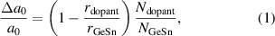
Figure 2. XRD data obtained from the Ge1−y
Sny
samples. (a) 2Theta/omega scan of the (004) reflection for all samples, (b) 2Theta scan at ω = 3° of the samples with an offset of 100 between the graphs and (c) reciprocal space mapping (converted to lattice parameter) showing the asymmetric  4 reflections of the GeSn peaks and the relaxation lines.
Download figure:
Standard image High-resolution imagewhere  and
and  are the covalent radii of Sb and Ge1−y
Sny
, respectively. The parameter
are the covalent radii of Sb and Ge1−y
Sny
, respectively. The parameter  depends on the Sn concentration and needs to be adapted in each iteration. Furthermore,
  is the dopant concentration in 1 cm−3 and
  is the number of Ge1−y
Sny
atoms per cm3 [21, 22]. Additionally, we performed a 2Θ scan at ω = 3° to obtain information about the polycrystalline proportion of the Ge1−y
Sny
layer (figure 2(b)). Our analysis shows an increase of the polycrystalline proportion of the layer with increasing Sn concentration.
is the number of Ge1−y
Sny
atoms per cm3 [21, 22]. Additionally, we performed a 2Θ scan at ω = 3° to obtain information about the polycrystalline proportion of the Ge1−y
Sny
layer (figure 2(b)). Our analysis shows an increase of the polycrystalline proportion of the layer with increasing Sn concentration.
The dopant concentration as well as sample mobility were obtained from Hall measurements at sample temperatures of 10 K and 300 K (table 2). Since the Ge1−y Sny layer is degenerately doped its temperature-dependent resistance is similar to that of a metal. By cooling down the samples to 10 K, contributions from the Si substrate are frozen out and data for the carrier concentration inside the Ge1−y Sny layer can be obtained with greater accuracy. Since the optical measurements are carried out at room temperature, we also report the Hall data for sample temperatures of 300 K. At this temperature, no reliable data could be extracted for the sample with the highest Sn concentration. Temperature dependent Hall data is shown in more detail in the supplementary information (available online at stacks.iop.org/JPD/54/445109/mmedia). While the nominal sample doping is constant at ND = 1 × 1020 cm−3, the concentration of active charge carriers can be seen to decrease as the Sn content is increased. The mobility also decreases with increasing Sn concentration. Most notably, the mobility obtained at T = 10 K drops by three orders of magnitude for the sample with the highest Sn concentration, indicating a decrease in material quality as well as an increase of alloy scattering [21].
Table 2. Compositional information obtained from XRD analysis and carrier concentrations as well as mobilities obtained from Hall measurements.
| Sample A | Sample B | Sample C | Sample D | ||
|---|---|---|---|---|---|
| Sn content (XRD)/% | 0.0 | 2.0 | 4.5 | 7.6 | |
 (calculated) (calculated) | 16.0 | 16.2 | 16.4 | 16.6 | |
| m* (calculated) | 0.12 | 0.0972 | 0.07149 | 0.05141 | |
| T = 10 K | ND (Hall)/cm−3 | 9.04 × 10¹⁹ | 8.54 × 10¹⁹ | 8.54 × 10¹⁹ | 6.20 × 10¹⁹ |
| μ (Hall)/cm2/Vs | 141 | 110 | 101 | 0.49 | |
| T = 300 K | ND (Hall)/cm−3 | 9.50 × 10¹⁹ | 1.17 × 10²⁰ | 1.19 × 10²⁰ | — |
| μ (Hall)/cm2/Vs | 117 | 76 | 68 | — | |
| a0/Å | 5.66 | 5.67 | 5.69 | 5.72 | |
Assuming that the permittivity of the Ge1−y Sny layer can be well represented by a Drude term of the form
where  is the high-frequency permittivity,
  is the plasma frequency and
  is the scattering rate, we can utilize the measured dopant concentrations and motilities to predict values for the Drude parameters
  and
and  based on our Hall measurement results according to
This requires us to assume values for  and m* for different Sn concentrations. Values for
  are usually obtained from linear interpolation between values for pure Ge and pure Sn [8], the results of this interpolation are shown in table 2. For our material, we can assume that the main contribution to Hall measurement results originates from electrons in the indirect L conduction band valley. Following again the approach adopted in [8], we obtain the effective masses for electrons in the alloyed samples from linear interpolation between the effective masses of the constituent elements.
4. Optical characterization results and discussion
Studying the infrared reflectivity is one of the standard methods to investigate the optical properties of materials [23, 24]. Here, we used both reflectivity data from unstructured samples and transmission data from structured grating antennas as two different approaches to obtain Drude parameters for different samples.
The results of the FTIR reflectivity measurements are shown in figure 3. All measurements are normalized to the reflectivity spectra obtained from an Ag mirror. The data were fitted using a three-layer model, where the permittivity of the Ge1−y
Sny
layer was modelled by a Drude term of the form shown in equation (2). The thickness of the Ge1−y
Sny
layer was used as an additional fitting parameter to account for local thickness variations resulting from the MBE growth. The Si substrate permittivity was, again, considered as a fitting parameter in a range of 9 ⩽  1 ⩽ 13 (setting 2 = 0.1) to account for wafer-dependent variations in the dopant concentration.

Figure 3. Reflectivity spectra (solid lines) and fitting functions (dashed lines) for samples A–D. Data obtained in the spectral range marked as dark blue was included in the fitting with a weight factor of ten, data in the spectral range marked as light blue was included with a weight factor of one.
Download figure:
Standard image High-resolution imageFor our antennas, an accurate modelling of the material properties at resonance wavelengths λ > 10 µm is particularly relevant. This relies on precise modelling of the reflectivity at wavenumbers at or below the plasma edge (figure 3). To get the best accuracy in the desired wavelength region, a weighting factor of 10 was used for the measured data in the range from 1000 to 2250 cm−1. The range of 630–5000 cm−1 was weighted with a factor of 1 and the remaining data was not taken into account. These wavelength ranges are indicated in figure 3 as darker and lighter shades of blue. Figure 3 shows the reflectivity spectra and the fitting functions for the four samples. All reflectivity spectra clearly show a plasma edge at wavelengths that, contrary to expectation, do not vary significantly with Sn content.
Prior to discussing the influence of Sn content on plasma wavelength and relaxation time in more detail based on the fitting results, we present the extinction spectra obtained from transmission measurements through the Ge1−y
Sny
grating antennas. The normalized extinction  of the comb-like antennas was extracted from transmission data as
  , where
  is the transmission through the structured Ge1−y
Sny
grating antennas on top of the Si Substrate and
is the transmission through the structured Ge1−y
Sny
grating antennas on top of the Si Substrate and  is the background transmission measured through the Si Substrate alone [7]. The extinction spectra show distinct peaks at wavelengths between 11 and 19 µm (figure 4). Simulations reveal that this peak originates from a plasmonic mode propagating along the antenna, with hotspots at the antenna/substrate interface (figure 1(b)). The extracted peak positions shift to higher wavelengths with increasing grating pitch and show a very weak trend towards lower wavelengths for a fixed geometry as the Sn content is increased (table 3). Furthermore, the peak height can be seen to decrease with increasing Sn concentration. Indeed, the extinction spectra become almost flat for sample D with the highest Sn concentration as a result of the strong decrease in sample quality that could also be seen in the carrier mobility data and the XRD analysis.

Figure 4. Extinction spectra for all antenna geometries.
Download figure:
Standard image High-resolution imageTable 3. Peak positions obtained from the extinction spectra for all antennas.
| Geometry | 1 | 2 | 3 | 4 | 5 | 6 |
|---|---|---|---|---|---|---|
| 0% Sn (cm−1 µm−1) | 809/12.4 | 833/12 | 752/13.3 | 659/15.1 | 597/16.7 | 539/18.5 |
| 2% Sn (cm−1 µm−1) | 833/12 | 802 /12.5 | 752/13.3 | 671/14.9 | 605/16.5 | 543/18.4 |
| 4.5% Sn (cm−1 µm−1) | 844/11.8 | 836/12 | 763/13.1 | 701/14.3 | 609/16.4 | 539/18.5 |
| 7.6% Sn (cm−1 µm−1) | 906/11 | 771/13 | 779/12.8 | 713/14 | 624/16 | 586/17 |
We used an RCWA-based fitting procedure to extract Drude parameters directly from the best fit to the extinction spectra. Simulated extinction spectra for geometry 2 are shown in figure 5 together with measured spectra. Values for plasma wavelengths and relaxation times obtained for all samples from electrical measurements and from fits to the optical data are summarized in table 4.

Figure 5. Comparison between measured and simulated extinction spectra for a grating with a pitch of 3 µm and a width of 1.2 µm (geometry 2) using different Drude parameters.
Download figure:
Standard image High-resolution imageTable 4. Plasma wavelengths  and relaxation times
  obtained for all samples based on electrical as well as optical measurements.
| Sample A | Sample B | Sample C | Sample D | ||
|---|---|---|---|---|---|
| Hall data (300 K) |

| 4.75 | 3.87 | 3.31 | — |

| 7.98 | 4.20 | 2.76 | — | |
| Hall data (10 K) |

| 4.87 | 4.41 | 3.77 | 3.84 |

| 9.6 | 5.7 | 3.8 | 0.01 | |
| Reflectivity spectra |

| 6.14 | 6.12 | 6.63 | 7.2 |

| 10.8 | 7.1 | 11 | 5.7 | |
| RCWA fit to extinction spectra |

| 6.42884 | 6.69862 | 6.64193 | 6.17186 |

| 13.16 | 8.508 | 7.628 | 5.178 |
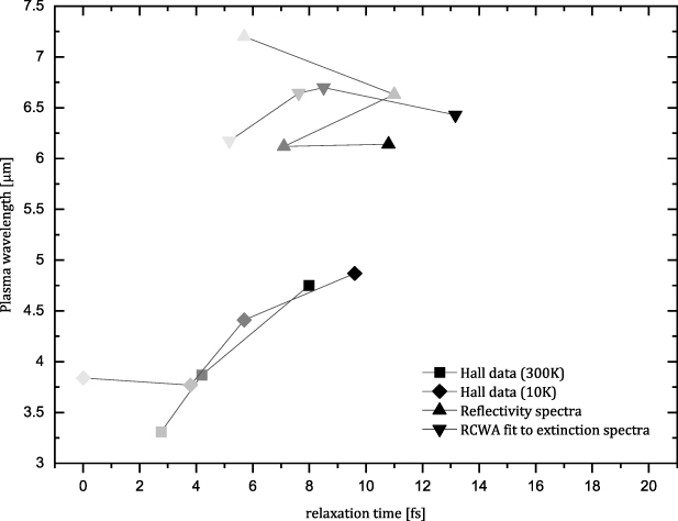
Given the fact that the dopant concentration in our samples is approximately constant, as shown by Hall measurement results (table 2), we can expect an increasing Sn content to lead to a decrease in plasma wavelength as a result of the decrease in effective electron mass. However, this is not supported by data obtained from optical measurements. For a better visualization of the influence of Sn content on plasma wavelengths and relaxation times and in order to identify possible trends, the results for those two parameters for all samples and for the different extraction methods used are also mapped out in figure 6. While the plasma wavelengths for the samples with highest Sn content are predicted to be well below 4 µm based on Hall data, optical data shows the plasma wavelengths to be above 6 µm for all samples. Indeed, while the plasma wavelengths and relaxation times obtained from the different optical measurements show good agreement, the parameters extracted from Hall measurements are notably different. In particular, those measurements severely underestimate the plasma wavelength and predict lower relaxation times. It has been pointed out in previous investigations that the DC mobility is a poor measure for losses in plasmonic structures at mid-IR wavelengths [5], however, the large differences in plasma wavelengths as predicted by Hall measurements and as obtained from optical measurements are striking. One possible explanation for the strong discrepancy between optical and electrical measurements is the high defect density within the samples, which can contribute to unintentional doping. Furthermore, future investigations could include SIMS measurements in order to verify the vertical doping profiles of our samples.
Figure 6. Map of the extracted plasma wavelengths and relaxation times obtained from electrical and optical measurements for samples A–D with different Sn concentrations. Here, the Sn content is indicated by the color gradient, varying from black (0% Sn, sample A) to lightest gray (largest Sn content, sample D).
Download figure:
Standard image High-resolution image
We find that the agreement between simulated and measured extinction spectra is good for simulations based on Drude parameters obtained from FTIR reflectivity spectra, taking into account the fact that the signal-to-noise ratio degrades for the measured signal at wavelengths above 15 µm due to the FTIR detector (figure 5). Furthermore, we attribute the presence of a shoulder in the measured spectra at wavelengths around 8.5 µm to the presence of the SiO2 layer above the gratings, which is not accounted for in the simulation. The simulation results based on Hall data, however, predict extinction spectra with higher peaks and more sharply defined resonances that are markedly different from the measurement results.
When focusing on the results for plasma wavelength  and relaxation time
  obtained from optical measurements alone, we find that, while
  is only weakly influenced by the Sn content,
  shows a marked decrease with increasing Sn concentration (figure 6), which we attribute to a decrease in material quality with increasing Sn content. The lattice mismatch between the doped Ge1−y
Sny
layer and the Si substrate below increases strongly with increasing Sn content, this can be expected to induce an increase in threading dislocations, in the polycrystalline proportion and other crystal defects, leading to the decrease in
shows a marked decrease with increasing Sn concentration (figure 6), which we attribute to a decrease in material quality with increasing Sn content. The lattice mismatch between the doped Ge1−y
Sny
layer and the Si substrate below increases strongly with increasing Sn content, this can be expected to induce an increase in threading dislocations, in the polycrystalline proportion and other crystal defects, leading to the decrease in  . While it is advantageous from a fabrication point of view to deposit Ge1−y
Sny
layers directly on Si, we find that this growth strategy degrades material quality to a point where the incorporation of Sn actually leads to decreasing antenna performance, as can be seen from the decreasing peak height of the extinction spectra with increasing Sn content (figure 4). Finally, we note that while a constant relaxation time is sufficient to model the extinction spectra observed from our plasmonic gratings, a frequency-dependent scattering rate should be assumed for a more accurate estimation of plasmon decay times [5].
. While it is advantageous from a fabrication point of view to deposit Ge1−y
Sny
layers directly on Si, we find that this growth strategy degrades material quality to a point where the incorporation of Sn actually leads to decreasing antenna performance, as can be seen from the decreasing peak height of the extinction spectra with increasing Sn content (figure 4). Finally, we note that while a constant relaxation time is sufficient to model the extinction spectra observed from our plasmonic gratings, a frequency-dependent scattering rate should be assumed for a more accurate estimation of plasmon decay times [5].
5. Conclusion
We investigated the influence of Sn content in highly n-doped Ge1−y Sny layers on Si with Sn concentrations varying between 0% and 7.6% on plasma wavelength and relaxation time by extracting those parameters from three different characterization methods (Hall measurements, FTIR reflectivity data on unstructured samples and FTIR transmission data on structured samples). Our analysis extends results of a previous investigation of n-doped Ge1−y Sny alloys for plasmonic applications, which was limited to alloys with a Sn content of 5% and dopant concentrations of 3.6 × 1019 cm−3 or less. Our results show that modelling the permittivity of our highly doped Ge1−y Sny layers with a simple Drude approach is sufficient to predict extinction spectra for plasmonic grating antennas with reasonable accuracy. The Ge1−y Sny layers were deposited directly on Si for ease of fabrication, however, this leads to a strong degradation of material quality and, thus, a reduced peak height at resonance in extinction spectra compared to antennas made from Ge. This contradicts the expected performance increase due to the lower electron masses in the alloyed semiconductor Ge1−y Sny .
The advantages of highly doped Ge1−y Sny compared to Ge for plasmonic applications can only be leveraged if the material quality can be improved. Previous studies on highly doped Ge have found that laser annealing is particularly effective in not only increasing the concentration of electrically active charge carriers but also in improving overall material quality [23, 25]. This could, therefore, also be a strategy to obtain high-quality doped GeSn layers. Finally, combining in-situ with ex-situ doping strategies could be a means to further tune material properties [26].
Data availability statement
All data that support the findings of this study are included within the article (and any supplementary files).