
Abstract
In this study, we investigate a Schottky junction based on solution-processed multilayered graphene (MLG). We present a rectifying device obtained with a straightforward approach, that is drop-casting a few microliters of MLG solution simultaneously onto Si, Si–SiO2 and Si–SiO2–Cr/Au surface. Monitoring the modulation of Schottky barrier height while operating in reverse bias, we study the behavior of such prepared MLG-Si/junction (MLG-Si/J) when exposed to oxidizing atmosphere, especially to nitrogen oxide (NO2). We finally compare the sensing behavior of MLG-Si/J at 1 ppm of NO2 with that of a chemiresistor-based on similarly prepared solution-processed MLG. Our study thus opens the path towards low-cost highly sensitive graphene-based heterojunctions advantageously fabricated without any complexity in the technological process.
Export citation and abstract BibTeX RIS

Original content from this work may be used under the terms of the Creative Commons Attribution 4.0 license. Any further distribution of this work must maintain attribution to the author(s) and the title of the work, journal citation and DOI.
1. Introduction
In the past decade, graphene has been proposed to form Schottky junction with a large variety of semiconductors such as Si, GaAs [1, 2], SiC [1, 3–5], GaN [6], CdS [7], CdSe [8]. Such hetero-junctions can be widely used in (opto)electronic applications, e.g. photodetectors [9–11], solar cells [12–14] and barristors [15]. In those applications, graphene can play the role of the metals because of the high mobility in both suspended and unsuspended layers, up to 2.5 × 10⁴ or 2.0 × 105 cm2 V−1·s−1, respectively [16–18]. Also, the transparency up to 98% in the visible range [19] would enable to lower the absorption of the light radiation typically generated by the metals. To ensure better performance of the devices in some of the aforementioned applications, high stability of the operating environment is strongly required. However, it is well known that graphene and its derivative is extremely reactive to the surrounding atmosphere [20–26]. The interaction with the ever-present gaseous species in the environment determines the shift of the Fermi level which results in the modulation of the Schottky barrier height (SBH) [15, 27]. While on one hand the SBH's modulation might influence the performance of some devices, on the other hand it does not necessarily represent a downside. Operating with the Schottky junction, the interaction with the surrounding gases can be such advantageous as a transduction mechanism in the sensing field that the Schottky junction between graphene and Si has been promisingly proposed for the detection of several analytes [28–34]. To realize the junction, graphene is usually produced by techniques such as chemical vapor deposition (CVD) [28, 30–34] or mechanical cleavage [29, 35]. In both cases, either the synthesis of the material needs complex equipment and fabrication processes, as for the CVD, or an extremely low throughput is obtained through the peel-off of the graphite by mechanical cleavage [36].
In the current study, we fabricate the junction using the material synthesized in a low-cost alternative way, i.e. liquid phase exfoliation (LPE) of natural graphite. Although the solution-processed materials can result in dispersions with a certain distribution of the flakes' thickness and size [37, 38], we aim at fabricating both material and device more straightforwardly and with much less technologically complexity compared to the others described previously. We already reported the proof-of-concept of a similar device in previous works where we showed the behavior of the Schottky junction based on LPE-multi-layered graphene (later referred as MLG/Si-J) while interacting with an electron-donor analyte, such as ammonia (NH3) [39–41]. Up to now, besides those reports, LPE-based Schottky junction has been partly investigated by another group only, despite the method reported in that work is rather a combination of LPE and CVD [42]. Following-up our prior works, in this paper, we study the sensing properties of solution-processed MLG/Si-J when exposed to an electron-acceptor target gas, such as NO2. We also compare the sensing behavior of the Schottky junction with that of a solution-processed MLG-based chemi-resistor (CR), proving that the transduction mechanism relied on the SBH modulation is definitively more efficient compared to the change of resistivity induced in the CR. Our results are therefore consistent with those reported by Singh et al [31], even though originally obtained with a solution-processed low-cost-based MLG/Si-J.
2. Materials and methods
We investigated MLG through a Renishaw inVia Reflex spectrometer equipped with an Ar laser (λ = 514.5 nm) and a 100× objective with a numerical aperture of 0.70. The surface topography was inspected through scanning electron microscope (SEM) Philips XL50, using a beam acceleration voltage of 15 kV.
To fabricate the Schottky junction, we adopted the structure depicted in figures 1(a) and (b) [43, 44]. As a substrate, we used an n-type heavily doped Si wafer (ρ = 1 Ωcm) covered with e-beam evaporated SiO2 film (250 nm) excluding a square window of 16 mm2. Around the Si window, onto the SiO2 film we evaporated a Cr/Au (10 nm/100 nm) annulus, having the inner side 6 mm long. On the backside of the Si wafer, we deposited by e-beam an alloy of Ti/Pd/Ag serving as ohmic contact.
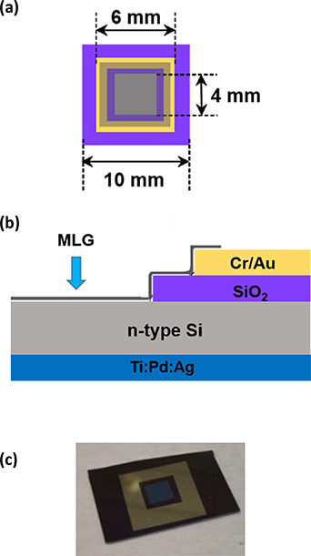
Figure 1. (a) Planar, (b) lateral view and (c) optical image of the fabricated device. The blue arrow in panel (b) indicates where MLG is in contact with Si to form the hetero-junction.
Download figure:
Standard image High-resolution imageWe synthesized MLG dispersing 2.5 mg of natural powdered graphite (Sigma-Aldrich, product 332461) in a mixture of 2-propanol and water used as a solvent to exfoliate the graphite [45]. After the exfoliation and purification steps detailed in previous reports [45, 46], we drop-casted few microliters of the MLG feed solution over the whole structure, simultaneously covering the Si window and the surrounding top electrical gold contact (figures 1(a) and (b)). MLG/Si-J is formed where MLG is in intimate contact with Si, as indicated by the blue arrow in figure 1(b). Figure 1(c) displays the optical image of the fabricated device.
The electrical analysis was performed by a Keithley 4200 Semiconductor Characterization System connected to a Cascade Microtech Summit 11000 probe station, in ambient conditions at room temperature.
Afterwards, we exposed the device in a customized gas sensor characterization system comprising a stainless-steel chamber (0.4 dm3) placed in a thermostatic box and provided with an electrical grounded connector for bias and conductance measurements. Temperature, pressure, relative humidity and flow rate of the analyte were kept constant at (22 ± 2) °C, (1.00 ± 0.05) bar, 50% and 500 sccm, respectively. Different concentrations of the analytes were obtained by a programmable mass flow controllers (MKS) and electro-pneumatic valves. During the measurements, we polarized the MLG/Si-J at a reverse constant DC voltage of −3 V with a Precision Power Supply TTi QL355 T. The current values were recorded by a high-resolution pico-ammeter (Keithley 6485).
3. Results and discussion
Figure 2 shows the results of the morphological characterizations performed on solution drop-casted onto the substrate. Figure 2(a) displays the representative Raman spectrum of the solution while figure 2(b) is the magnification of the 2D band, located at ∼2700 cm−1. The profile, the features of the bands and the relative ratio of the deconvolved Lorentzian sub-components 2D1 (green line in figure 2(b)) and 2D2 (red line in figure 2(b)) indicate that the material forming the Schottky junction is mostly composed by MLG with a minimum thickness of 2–3 nm [39–41, 45–51]. The multilayered and jagged nature of the material is confirmed by the SEM image reported in figure 2(c) [48].

Figure 2. (a) Representative Raman spectrum of MLG, normalized to the intensity of the G band. (b) Magnification of the 2D band of panel (a) with the sub-components 2D1 (green line) and 2D2 (red line), located at ∼2695 cm−1 and ∼2726 cm−1, respectively. (c) SEM image captured on MLG drop-casted on the substrate. Reproduced from [48]. © Royal Society of Chemistry. CC BY 3.0.
Download figure:
Standard image High-resolution imageFigure 3 shows the I–V characteristic of the MLG/Si-J after drop-casting the MLG solution onto the bare device. For comparison, the I–V curve of the bare device is reported in the Supporting Information (figure S1 (available online at stacks.iop.org/JPD/54/375104/mmedia)). MLG/Si-J exhibits a Schottky diode behavior (figure 3(a)) with a rectification factor of about 100, as determined by the I–V characteristic in semi-logarithmic scale (inset figure 3(a)). The current I is expressed by the equation (1)) based on the thermionic emission model:
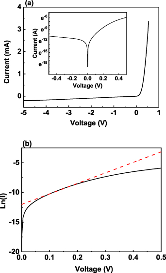
Figure 3. (a) I–V characteristic of the MLG/Si-J in linear and semi-logarithmic scale (inset). (b) Semi-logarithmic plot of the forward biased current with overlapped linear fit (red dashed line) to extract the factor of ideality η.
Download figure:
Standard image High-resolution imagewhere A is the MLG/Si-J contact area, A* the effective Richardson's constant for Si substrate, T the absolute temperature, ϕB the SBH, q the electron charge, kB the Boltzmann constant, V the bias voltage and η the ideality factor of the diode [52].
For V≫ ηkB
T/q, equation (1) can be rewritten as  , where Is is the saturation current [52], and rearranging the terms, the previous equation becomes:
The linear fit of equation (2), in the range 75 ÷ 200 mV, enables to determine the ideality factor η and the saturation current Is. The limits of the voltage range are determined by the value 3kB T/q satisfying the conditions V ≫ ηkB T/q (with η = 1) and the voltage where the series resistance starts dominating, respectively [52].
From the slope of the fit (figure 3(b)), we extract η ∼ 2.25, which is higher than the value of the ideal Schottky junction (η = 1). Values of η greater than 1 are usually attributed to the inhomogeneity at the interface with Si which determines deviations from the pure thermionic emission transport [1, 9, 34, 53–56]. Nevertheless, values comparable or much higher than the one reported herein have been largely reported in the literature, also in the case of graphene synthesized through different techniques, such as CVD [31, 32, 57, 58].
Manipulating the equation describing the saturation current  , whose value is determined from the intercept of the straight line with the y-axis (figure 3(b)), we obtain ϕB from the equation (3):
If we assume the entire uncovered Si window (A = 0.16 cm2) as a MLG/Si-J contact area, kB T/q = 26 mV at T = 300 K and A* = 112 A cm−2 K−2 for n-Si substrate, we estimate the absolute value ϕB ∼ 0.68 eV which is aligned with the values reported elsewhere [9, 14, 59]. Because of the drop-cast technique used to create the Schottky junction, it can happen that the contact area between the MLG feed solution and Si slightly differs from the nominal area of the Si window. The contact area parameter, however, does not dramatically affect the value of ϕB. We estimate that a large variation of A from 16 down to 9 mm2, that is the area in case the Si window was 3 mm long in lateral side, would result in a decrease of ϕB ∼ 1%. Therefore, minimal variations of A induce negligible changes of SBH.
The determination of ϕB permits to calculate the work function of MLG (later referred as WG), according to the Schottky–Mott relation WG = ϕB + χSi, where χSi = 4.05 eV is the electronic affinity of Si.
The estimated value in our case (WG ∼ 4.73 eV) is slightly higher than that usually reported for graphene, ranging between 4.3 and 4.6 eV, depending on the number of layers [60]. Provided that WG also depends on the bias voltage [61], the small deviation of WG might be ascribed to both the multi-layer nature and/or the p-doping of the material. Indeed, the MLG considered in this paper differs significantly from the material used in other works, e.g. graphene synthesized by CVD [62] or epitaxially grown on 6H-SiC [60, 63, 64]. Those techniques, although much more technologically complex and more expensive than LPE, usually guarantee a more accurate control of the number of layers. Yet, the inhomogeneity of the flakes' thickness usually associated to the solution-processed materials [37, 38] might influence some electrical parameters of the junction and the subsequent performance upon the analyte exposure.
Once the electrical properties were characterized, we investigated the sensing properties of MLG/Si-J in oxiding atmosphere using NO2 as a target gas. We operated in reverse bias (−3 V) because of the exponential dependence of the saturation current from the SBH which is affected by the molecular absorption of NO2, as reported in equation (1) [31].
Figure 4 shows the behavior of the saturation current when the device was exposed to 2 parts-per-million (ppm) of NO2. When we injected the analyte into the test chamber (pale blue rectangle in figure 4), the signal keeps increasing for 10 min up to reach the maximum value Imax when the gas flow is interrupted. During the subsequent purge phase with N2, the signal spontaneously and slowly tends to restore the initial state.

Figure 4. Real-time current behavior of MLG/Si-J upon exposure to 2 ppm of NO2. The graph is normalized at the value of the current at the gas inlet. The pale blue rectangle highlights the exposure window.
Download figure:
Standard image High-resolution imageThe real-time behavior is comparable with the results reported in previous works [46–50, 65–70], especially in terms of the kinetics of interaction between the sensing layers and the molecules during both exposure and purging phase. While in those works the authors reported on chemi-resistive devices, where the charge transfer induced a variation in the resistivity of the sensing layer, in the present paper, the behavior of the current is based on the SBH's modulation due to the interaction between the analyte and the MLG-Si/J [9]. The increase of IS means a higher injection of the minority carriers (i.e. electrons) from p-doped MLG to the n-type Si. The IS increase can be attributed solely to the lowering of SBH at the end of the adsorption process, as sketched in figure 5. In that figure, to easily visualize the physical mechanism and without lack of generalization, we draw up the bands of a single layer of graphene even though we are dealing with a mixture of multilayered material.

Figure 5. Band diagram of the heterojunction (a) before and (b) after the exposure to NO2. For the sake of clarity, the band structure of graphene was designed similar as that of a single layer of graphene. Evac, EC, EV and EF indicate vacuum energy, conduction band, valence band and Fermi level of the n-type Si, respectively.
Download figure:
Standard image High-resolution imageCompared to the pre-exposure (figure 5(a)), it can be seen that the holes donated by the NO2 during the adsorption process recombine at the interface MLG-Si. Consequently, SBH (ϕB') was lower (figure 5(b)) than the pre-exposed condition, as also reported by Singh et al [31], and the flow of electrons is favored from the p-type side of the junction, determining the increase of IS.
Applying equation (3) to the graph in figure 4, we explicitly calculated the variation of the SBH induced by the exposure to 2 ppm of NO2 as follows:
where I0 is the current immediately prior to the gas inlet (figure S2 (available online at stacks.iop.org/JPD/54/375104/mmedia)). The negative value of the SBH's variation (ΔϕB∼ −2.5 meV) further indicates that ϕB' < ϕB, i.e. SBH after the exposure is lower than SBH before the exposure. To strengthen more this conclusion, we exposed the MLG-Si/J to decreasing concentrations of NO2 from 2 down to 0.4 ppm. Figure 6(a) shows the signal recorded during the exposure window at different concentrations of NO2. Introducing in equation (4) the values Imax/I0 determined from figure 6(a), we accordingly obtained the variation of SBH. The absolute value of SBH plotted as a function of NO2 concentration confirms our statement that the final SBH after each exposure is reduced compared to the pre-exposed situation (figure 6(b)).
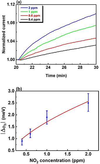
Figure 6. (a) Magnification of the signal recorded during the exposure at different concentrations of NO2. The signals are normalized at the values I0 prior to the gas inlet. (b) Absolute value of SBH vs NO2 concentration as calculated from panel (a).
Download figure:
Standard image High-resolution imageThe fit in figure 6(b) (red line) shows the dependence of SBH from the concentration C given by ΔϕB ≈ Cα , where we extrapolated α = 0.6 ± 0.1. Such a correlation, besides being in close agreement with our previous results obtained with other analytes [40], is well aligned with the outcomes reported in the literature, independently from the technique of graphene synthesis [15, 43, 71].
To finally illustrate the role of the SBH in the sensing mechanism of MLG-Si/J, we compared the behaviour of the junction with that of a CR. We thus referred to the device reported in our previous work [48], where MLG was synthesized via LPE using the same recipe as described in the present paper. The only difference between MLG-Si/J and CR is that, in case of CR, we fully covered the Si-bare substrate with a thin layer of SiO2 before drop-casting MLG to insulate the metallic electrodes and sensing layer from Si. Despite the deposition of MLG on top of either Si or SiO2, no differences in the wettability of MLG on both substrates were observed, fairly enabling the comparison of the two devices.
Figure 7 displays the representative dynamic behavior of CR and MLG-Si/J upon exposure to 1 ppm of NO2. It can be observed a significant difference between the black and red curve during the exposure window, i.e. (ΔI/I0)MLG-Si/J ≈ 3.3(ΔI/I0)CR. Because of the use of the similar solution-processed MLG in both cases, it is very likely that the difference can be ascribed to the mechanism of transduction taking place in either architectures. In MLG-Si/J operating in reverse bias, IS exponentially depends on the SBH's modulation which is the parameter affected by the adsorption of the analyte's molecules. Conversely, in CR, the conductance variation is more linearly dependent from the analyte adsorption.

Figure 7. Percentage variation of the current vs time of MLG/Si-J (red line) and CR (black line) during the exposure to 1 ppm of NO2 (pale blue rectangle). Inset: picture of the MLG-based CR [48]. Reproduced from [48]. © Royal Society of Chemistry. CC BY 3.0.
Download figure:
Standard image High-resolution image
It is well known that the solution-processed materials might introduce a small degree of uncertainty in the features of both material and physical quantities of the devices. Nevertheless, although withdrawn with LPE-based MLG, our conclusions are not only independent from the techniques used to synthesize the sensing layer but also intrinsically due to the physics of the investigated devices. Furthermore, our achievements reveal particularly appealing as can be tailored without any complex fabrication process and tool.
4. Conclusions
We fabricated a Schottky device depositing few microliters of solution-processed MLG. The current–voltage investigation confirmed that we successfully realized a MLG-Si/J with a rectifying ratio roughly equal to 100 and an ideality factor η = 2.25. Such prepared hetero-junction was sensitive to NO2 even at concentrations as low as 400 ppb. Analyzing the saturation current of the MLG-Si/J, we investigated the transduction mechanism relied on the SBH's modulation induced by the absorbed molecules. We finally compared the sensing behavior of MLG-Si/J with that of a CR-based on similarly prepared solution-processed MLG. We experimentally showed that, during the exposure at 1 ppm of NO2, MLG-Si/J exhibited a signal that is roughly three times higher than the CR one. Our outcomes thus pave the route to efficiently fabricate low-cost sensitive gas sensors without any complexity in the technological process.
Acknowledgments
The authors are grateful to E. Massera (ENEA Portici, Italy) for the assistance in the use of the sensing set-up.
Data availability statement
All data that support the findings of this study are included within the article (and any supplementary files).
Author contributions
F R fabricated the devices, performed the sensing measurements, analysed the data, wrote the original draft, reviewed and edited the manuscript. M A N assisted with the electrical measurements. R M performed the electrical measurements. M A N and R M assisted in the interpretation of the electrical measurements. M L M synthesized the sensing material. T P conceived the idea of the experiment, assisted with the fabrication of the devices, the interpretation of the sensing measurements, the outline of the manuscript and supervised the final draft. All authors have read and agreed to the published version of the manuscript.