

Abstract
Solution-processed organic/inorganic hybrid halide perovskites are a class of very promising photovoltaic materials because of their extraordinary optoelectronic properties. However, numerous intrinsic defects within perovskite films limit the performance enhancement of perovskite solar cells (PSCs). Herein, we introduce three different alkali metal fluoride additives into the perovskite precursor to modulate the defect behaviors. The addition of alkali metal fluorides, especially potassium fluoride (KF), significantly passivates grain boundaries and point defects within bulk perovskite films, contributing to increased carrier lifetime and reduced defect state density. By optimizing the concentration of additives, the PSC device with 1% KF added has realized a significantly enhanced power conversion efficiency of 20.11%, and ignorable hysteresis.
Export citation and abstract BibTeX RIS
1. Introduction
Solution-processed organic/inorganic hybrid halide perovskites have been recognized as a class of promising photovoltaic materials due to their fascinating properties, such as an ultralow fabrication cost [1], a tunable bandgap [2] and long carrier diffusion length [3], leading to the rapid development of perovskite solar cells (PSCs). Recently, the power conversion efficiency (PCE) of PSCs has gained a certified 25.5% [4], almost catching up with crystalline silicon counterparts. Despite the unprecedented achievements in photovoltaic performance, there still exist intrinsic imperfections that limit the further improvement of PSCs. The key challenge is the structural instability caused by numerous defects, including grain boundaries (GBs) and various point defects in bulk perovskite films. The GBs act as effective recombination centers [5], which increase the recombination probability of charge carriers [6]. Research also demonstrates that GBs are significant barriers to charge transport, and that a larger grain size with fewer GBs is beneficial for charge transport [7–10]. Besides, point defects, especially halide anion and organic cation vacancies, also play very important roles owing to their low formation energies [11, 12]. Though these point defects are proved to create shallow level traps [13], they still cause unwanted effects on the hysteresis of PSCs under an applied electric field [14]. To make things even worse, the formation of these point defects are accompanied by cations and anions diffusing to GBs [15]. The synergy between GBs and these point defects can cause the acceleration of nonradiative recombination [16] and induce the degradation of perovskite material and interfaces due to decomposition reactions [17]. Therefore, further research on how to reduce the GBs and control the formation of point defects within perovskite films is of vital significance to obtain more efficient and stable PSCs.
In an effort to achieve this goal, additive engineering is found to be an effective strategy. Some alkali-metal-cation additives have been demonstrated to significantly passivate the defects. Fang et al demonstrated that the nonradiative recombination is significantly reduced via lithium doping due to the generation of free electrons and the subsequent trap filling [18]. Bi et al found that those Na+ rich GBs contribute to a prolonged PL lifetime and reduced defect density, suggesting the effective passivation of detrimental GBs [19]. Cao et al reported that potassium iodide (KI) has a positive effect on passivating halide vacancies by suppressing the I− diffusion, according to DFT calculation [20]. On the other hand, much work also focuses on exploring anionic alternatives. Cl− has been frequently introduced to perovskite films in various forms, such as MACl [21], and NH4Cl [22], which alters the electronic properties of films and passivates defect-induced traps at interfaces and GBs. Only recently, Li et al demonstrated that fluoride ions have a more significant effect than Cl− and Br− for passivating halide anion and organic cation vacancies simultaneously, owing to the formation of strong ionic bonds with Pb2+ in the perovskite film and hydrogen bonds (N-H•••F) with MA+/FA+ cations [15].
However, the fundamental passivation mechanism of alkali metal cations still remains controversial. Moreover, there has been no research yet exploring different alkali metal cations combined with fluoride ions to figure out the passivation potential of defects. Here, we introduce three different alkali metal fluorides as perovskite precursor additives. The existence of Li+, Na+ and K+ in the bulk perovskite contributes to the increased crystallinity with reduced GBs. Moreover, defect state density is significantly reduced and carrier transport is improved. Due to the formation of the strongest ionic bonds between K+ and I− ions, the addition of KF achieves the most significant improvement in PSC performance by passivating GBs and suppressing the point defects in perovskite films.
2. Experimental section
2.1. Materials
SnCl4 · 5H2O (99.5%) and acetonitrile (ACN, 99.6%) were purchased from Alfa Aesar. Potassium fluoride (KF, 99.2%), dimethyl sulfoxide (DMSO, 99.9%), dimethyl-formamide (DMF, 99%), chlorobenzene (CB, 99.8%) and lead iodine (PbI2, 99%) were all purchased from Sigma-Aldrich. Methylammonium iodide (MAI), spiro-OMeTAD (99.5%), 4-tert-butylpyridine (4t-BP), PCBM (99.5%) and Li-bis-(trifluoromethanesulfonyl)imide (Li-TFSI) were all bought from Xi'an Polymer Light Technology. All these chemical reagents mentioned above are commercially available.
2.2. Characterization
The UV–vis absorption data were collected using an ultraviolet spectrometer (U-4100 Hitachi). The morphologies of MAPbI3 films were observed using the scanning electron microscope (SEM) (S-4800 Hitachi). The x-ray photoelectron spectroscopy (XPS) was measured by an AXIS Supra (Kratos), and the binding energy in XPS is corrected by aligning C 1s peaks. The steady-state photoluminescence (PL) and the time-resolved PL (TR-PL) spectra were obtained using the PL spectrometer (Fluo Time 300, Pico Quant), excited by a laser diode at a frequency and wavelength of 20 MHz and 372.3 nm, respectively. A light filter at 400 nm was utilized to filter out the excitation light. J–V characterization was conducted under AM 1.5 G conditions with a light intensity of 100 mW cm−2, using a solar simulator (94022A, Newport) and a sourcemeter (2400, Keithley). The J–V measurements were conducted by forward scan (from 0 to 1.2 V) and reverse scan (from 1.2 to 0 V), with a scan rate of 100 mV s−1. The external quantum efficiency (EQE) measurements were performed in the wavelength range of 300–850 nm, using an EQE measurement system (Model QEX10, PV Measurements).
2.3. Preparation of perovskite films
The perovskite precursor solution was prepared by dissolving 159 mg MAI and 461 mg PbI2 into the mixture of 71 μl DMSO and 635 μl DMF. The perovskite films with additives were fabricated with a certain amount of XF (X = K, Na and Li) added into the precursor solution. A series of samples were set up according to different concentrations of additives (0.25%, 0.5%, 1%, 2% and 4% molar ratio) in the precursor solution. Moreover, due to the bad solvability of KF, NaF and LiF in DMF or DMSO, the perovskite solutions with the additives were kept at 70 °C.
2.4. PSC device fabrication
Pristine ITO substrates were treated with the mixture of HCl and Zn powder. After that, they were carefully cleaned using distilled water, acetone, ethanol and isopropanol. For the electron transport layer (ETL), SnO2 film was deposited on these substrates by spin-coating at the rate of 3000 rpm for 30 s, using 40 μl SnCl4 · 5H2O/ethanol precursor with 29 mg ml−1 (0.083 mmol ml−1). After being heated at 150 °C for 30 min in air, the SnO2 layer was formed. The perovskite layers were deposited on the as-formed SnO2 layers, using the one-step spin-coating method. After the SnO2 substrates had been exposed to UV–ozone treatment for 900 s, the precursor solution was spin-coated on the SnO2 layer at 5000 rpm for 36 s. 1 ml of diethyl ether was continuously dripped on the spinning substrate at 16 s before the end of the procedure. After being annealed at 100 °C for 10 min, a dense perovskite film was formed. For the hole transport layer (HTL), a spiro-OMeTAD/CB (72.25 mg ml−1) solution was employed with 17.5 μl Li-TFSI/ACN (520 mg ml−1) and 28.75 μl 4t-BP added. The spiro-OMeTAD film was spin-coated on the as-formed MAPbI3 layer with a 3000 rpm rate for 35 s. Finally, the gold layer (100 nm) was thermally evaporated on the top under a vacuum (<1.0 × 10⁻³ Pa). The effective area of the cell is determined to be 0.1 cm2.
2.5. Electron-only device fabrication
The structure of the electron-only device is ITO/SnO2/ perovskite (without or with additives)/PCBM/Ag. The SnO2 and perovskite layers were fabricated with the same procedure as mentioned above. The PCBM precursor solution was prepared by dissolving 20 mg PCBM powder into 1 ml CB with 12 h of stirring. A PCBM layer was then deposited on the perovskite layer by spin-coating at 1000 rpm for 30 s, using 35 μl PCBM/CB precursor (20 mg ml−1).
3. Results and discussion
The top-view SEM images of different samples without or with additives (LiF, NaF and KF) are presented in figure 1. All the perovskite films are almost pinhole-free, with compact surface coverage (figures 1(a)–(d)). Moreover, we observe that those perovskite films with additives exhibit enlarged grain sizes compared to the control sample. The perovskite films with additives also have lower surface roughness, as shown in figure S1 (available online at stacks.iop.org/JPD/54/315504/mmedia). Correspondingly, statistical distributions of grain sizes for different samples are shown in figures 1(e)–(h). The average size of a perovskite film with LiF (175 nm) is comparable to the control sample. Importantly, significantly increased grain sizes of perovskite films have been obtained by the addition of NaF (235 nm) and KF (434 nm). By modulating the concentration of KF additive, the optimized morphology with large grains and no pin-holes is obtained with 1% KF (figure S2). It is known that large grains enhance carrier mobility [23]. Thus, the addition of KF may be more beneficial to the carrier transport. Moreover, since the GBs have been demonstrated to be effective recombination centers [24], the enlarged grain sizes with fewer GBs can also contribute to less trap-mediated recombination [23].
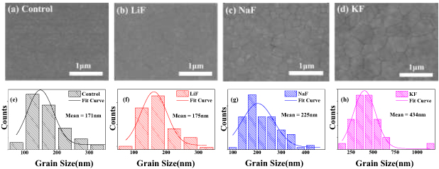
Figure 1. SEM images for samples without (a) or with the addition of (b) LiF, (c) NaF and (d) KF. The grain size distribution of perovskite films: (e) control, (f) with the addition of LiF, (g) NaF and (h) KF determined from the SEM images, with average grain size for each sample presented.
Download figure:
Standard image High-resolution imageX-ray diffraction (XRD) is used to further investigate the effect of alkali-metal-cation additives on the perovskite crystallization, as revealed in figure 2. All the XRD patterns of different samples demonstrate similar diffraction peaks corresponding to the tetragonal MAPbI3 phase [25] (figure 2(a)), indicating that the addition of alkali metal fluorides hardly alters the crystal structure. Besides, the diffraction peaks around 14° and 28° in samples with additives, which are ascribed to the MAPbI3 phase oriented along the (110) and (220) planes [25], have obviously increased compared with the sample without additives. The most significant improvement on the diffraction peak intensities is obtained at the solution concentration of 1% for KF (figure S3). In addition, when zooming in on the main peaks indexed to the (040) plane in figure 2(b), we observe a slight peak shift to a lower angle in the samples with additives, which may be attributed to the lattice expansion induced by the interstitial occupancy of alkali cations [26]. The full width at half maxima (FWHM) of (110) and (220) main peaks are shown in figures 2(c) and (d), respectively. The sample with LiF shows slightly smaller FWHM compared with the control sample, while the samples with NaF and KF exhibit much narrower widths, indicating the significant effect on enlarging grain sizes, based on the Williamson–Hall plot method [27]. The grain sizes calculated by this method are 55.3, 59.6, 74.4 and 104.6 nm for the control sample and samples with the additives of LiF, NaF and KF, respectively, in accordance to the trend of size distribution obtained from SEM analysis. The increased main diffraction peak intensity and reduced FWHM confirm that alkali-metal-cation additives are beneficial for the growth and crystallization of perovskite films.
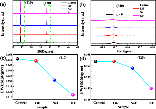
Figure 2. (a) XRD patterns of samples without or with additives, (b) the peak shift of (040) plane, the FWHM comparison of (c) (110) plane and (d) (220) plane for different samples.
Download figure:
Standard image High-resolution imageThe surface-sensitive XPS measurements are employed to verify the introduction of alkali metal cations into the perovskite films (figure 3). As displayed in figures 3(a)–(c), the peaks of Li 1s, Na 1s and K 2p are observed in the samples with additives. As we all know, XPS mainly collects information on the surface. The signals are also detected in the samples after the Ar+ etching, reflecting the existence of Li+, Na+ and K+ in the bulk region (figure S4). On the other hand, all the samples display two similar peaks around 619 and 630 eV (figure 3(d)), which are assigned to I3d in the perovskite. Similarly, peaks around 138 and 143 eV ascribed to the Pb 4 f7/2 and Pb 4 f5/2 are also observed in the samples in figure 3(e). Noticeably, there exist two pronounced shoulder peaks located around 136 and 140 eV, which are identified as a certain amount of metallic Pb0 in the control sample [28]. It is known that the existence of Pb0 represents the components of unsaturated Pb [29], which inevitably results in the removal of I and the formation of I vacancies [30]. However, after the introduction of metal alkali fluorides, the peaks of Pb0 have almost disappeared and the peak area ratio of Pb0/Pb4f has decreased to a great extent. The result indicates that I vacancies are reduced by the strong interaction between metal alkali cations and I− in the perovskite films. In short, the evident signals confirm that Li+, Na+ and K+ are successfully introduced into the samples, and moreover, they have suppressed the generation of I vacancies in the films.

Figure 3. The XPS of perovskite films with different additives: (a) Li 1s XPS spectrum of sample with LiF, (b) Na 1s XPS spectrum of sample with NaF, (c) K 2p XPS spectrum of sample with KF, (d) I 3d XPS spectra of samples without or with additives and (e) Pb 4f XPS spectra of samples without or with additives.
Download figure:
Standard image High-resolution imageCharge carrier recombination behaviors in the perovskite films are investigated by the PL and TR-PL measurements, as shown in figure 4. In this work, the PL measurements are conducted based on the glass/perovskite structure. The PL spectra in figure 4(a) demonstrate that an obvious increase in PL intensity is obtained by adding a certain amount of LiF, NaF and KF, which implies the effective reduction of nonradiative recombination. Moreover, the sample with KF yields the most significant increase in PL intensity. By optimizing the concentration of KF additive, the film shows the highest PL intensity at the concentration of 1% (figure S5). Besides, there is a slight enhancement in the absorbance of samples with additives, owing to better crystal quality. It can also be seen from the PL results and the UV–vis absorption spectra that the introduction of alkali metal fluorides into precursor solution does not alter the bandgap of perovskite films.

Figure 4. (a) The steady-state PL spectra/UV–vis absorption spectra, and (b) TR-PL spectra based on the glass/perovskite structure without or with LiF, NaF, KF in the films.
Download figure:
Standard image High-resolution imageFigure 4(b) presents the TR-PL spectra for different samples without or with additives. The PL decay curves are well fitted using a biexponential decay function, I(t) = A1exp(−t/τ1) + A2 exp(−t/τ2) + I0, where A1 and A2 represent the relative amplitudes, the fast decay component τ1 is related to the nonradiative recombination of surface traps near the GBs and the slow decay component τ2 is associated with nonradiative recombination within the bulk perovskite films [31]. As listed in table 1, the TR-PL fitting results illustrate that both τ1 and τ2 have a longer lifetime in the films with the additives. Among them, the sample with KF exhibits the longest carrier lifetime (τ1: 10.3 ns, τ2: 320 ns), which is much longer than the control sample (τ1: 6.49 ns, τ2: 161.17 ns). The results above demonstrate that the addition of alkali metal fluorides, especially KF, is able to effectively passivate GBs and point defects in bulk perovskite films, contributing to the reduction of carrier recombination [32].
Table 1. The fitted results of TR-PL spectra of samples without or with LiF, NaF, KF.
| Sample | τave (ns) | τ1 (ns) | Amplitude of τ1 | τ2 (ns) | Amplitude of τ2 |
|---|---|---|---|---|---|
| Control | 156.5 | 6.5 | 0.48 | 162.1 | 0.52 |
| LiF | 206.7 | 7.4 | 0.35 | 210.6 | 0.65 |
| NaF | 305.1 | 9.4 | 0.42 | 311.2 | 0.58 |
| KF | 316.2 | 10.3 | 0.32 | 320.9 | 0.68 |
Figure 5(a) illustrates the PSC device designed with a typical architecture, where the SnO2 film is the ETL, the spiro-OMeTAD is the HTL, and the gold is the top electrode. The perovskite films without and with additives are deposited on the etched ITO glass as the absorbing layer. Interestingly, the cross-sectional SEM image of the device with KF shows that the single grain grows oriented towards the normal direction of the interface and the vertical GB is almost negligible (figure 5(b)), which is expected to be beneficial to the charge extraction from the perovskite to the charge transport layers [33]. We have also demonstrated that the addition of K+ has a more pronounced effect on the improvement of film morphology than the other two alkali metal cations (figure S6). The J–V curves of completed PSC devices for different samples are shown in figure 5 (c) and the main photovoltaic parameters are listed in table 2. It can be seen that all the additives have contributed to the enhancement of device performance with enhanced short-circuit current densities (Jsc), fill factor (FF) and open-circuit voltage (Voc). Noticeably, the PCE of the device with KF (1%) is improved to 20.11%, with a 10.6% enhancement, mainly ascribed to the considerable improvement in FF and Voc. The FF of the sample with KF is improved from 0.73 to 0.77, with an increase of 5.4%, demonstrating better carrier transport because of advantageous changes in the morphology of perovskite film and enhanced charge conductivity induced by K+ [34]. The Voc is promoted from 1.11 to 1.14 V, with an enhancement ratio of 2.7%, thanks to the improved passivation effect and the effective reduction of electron–hole recombination. A slight enhancement of Jsc is also obtained, in agreement with the enhanced response in EQE measurement (figure 5(d)), which can be ascribed to the increased absorbance within the wavelength range of 450–800 nm (figure 4(a)). Besides, the improved charge transport induced by larger grain sizes leads to more carriers being collected, and also contributing to the enhanced Jsc [8]. In order to verify the effect of additives, we further fabricate 30 devices for each sample, and the statistical results exhibit good repeatability (figure S7). Besides, the PSC with KF also exhibits improved stability compared with those with other additives and the control (figure S8).

Figure 5. Photovoltaic performance of PSCs. (a) Schematic fabrication procedure for perovskite films with additives. (b) The cross-sectional SEM image of the PSC added with KF. (c) J–V curves of different device samples. (d) EQE measurements of PSC devices without or with additives.
Download figure:
Standard image High-resolution imageTable 2. The main photovoltaic parameters of the control device and devices with LiF, NaF and KF at the same concentration of 1%.
| Solar cell characteristics | ||||
|---|---|---|---|---|
| Sample | Jsc (mA cm−2) | Voc (V) | FF | η (%) |
| Control | 22.43 | 1.11 | 72.96 | 18.17 |
| LiF | 22.59 | 1.13 | 73.84 | 18.85 |
| NaF | 22.74 | 1.13 | 75.63 | 19.43 |
| KF | 22.94 | 1.14 | 76.91 | 20.11 |
Interestingly, the hysteresis of J–V curves reduces with the addition of alkali metal fluorides, as shown in figure 6. Moreover, with the increase in ionic radius from Li+ to K+, the hysteresis becomes smaller and almost disappears. We further calculate the hysteresis index (HI) to evaluate the variation of J–V hysteresis for different samples without or with additives in the following,
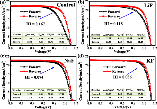
Figure 6. J–V curves in the forward/reverse scan directions for different samples without and with additives: (a) control, (b) with LiF, (c) with NaF, (d) with KF.
Download figure:
Standard image High-resolution imageThe HI of the control sample and the sample with LiF, NaF and KF is 0.167, 0.118, 0.074 and 0.036, respectively. Recently, experimental and theoretical studies indicate that the main ion migration process in perovskite is vacancy-mediated anion migration, such as I− migration [35], which should be the atomistic origin of J–V hysteresis in PSCs. Because of the charged nature of mobile anions, the selective introduction of ions can bond them in order to suppress the corresponding trap states [14]. However, due to the small size and relatively weak metallicity of Li+, it is unable to hinder I− migration effectively, thus the hysteresis is only to some extent suppressed. On the contrary, K+ is of a suitable size and has the strongest metallicity among these alkali metal ions. As a result, the addition of K+ could occupy the interstitial site perfectly and form the strongest ionic bonding with I−, leading to the significant suppression of the migration of I− ions and the most negligible hysteresis.
The space-charge-limited current (SCLC) measurement is a persuasive tool to calculate the trap state density (nt) of the perovskite films. The typical dark I–V curves for electron-only devices (figure 7(a)) show that samples with the addition of alkali metal fluorides have a lower trap-filled limit voltage (VTFL). Accordingly, the nt of the perovskite films can be evaluated based on the equation [36],
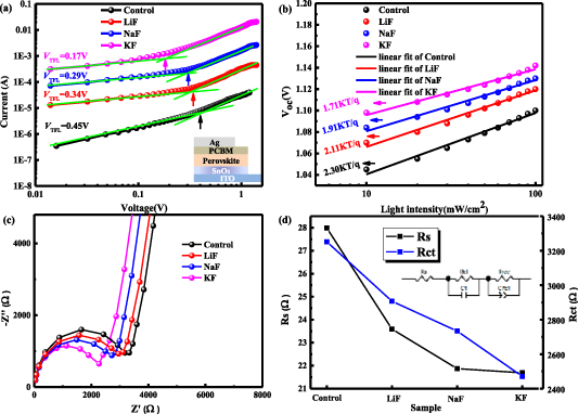
Figure 7. (a) Dark I–V curves of electron-only devices without and with additives. (b) The Voc of PSCs as a function of light intensity. (c) Nyquist plots for PSCs without or with different alkali metal fluorides. (d) The fitted plot of Rs and Rct for different samples.
Download figure:
Standard image High-resolution imagewhere  0 represents the vacuum permittivity, represents the dielectric constant of CH3NH3PbI3 ( = 28.8), e stands for the electron charge, and L denotes the thickness of MAPbI3 film. The control sample has a VTFL of 0.45 V with a relatively high nt of 8.1 × 1015 cm−3. The VTFL of samples with different additives (LiF, NaF and KF) are reduced to 0.33, 0.28 and 0.17 V, respectively. Correspondingly, the nt are calculated to be 5.9 × 10¹⁵, 5.0 × 10¹⁵ and 3.1 × 1015 cm−3, respectively. The hole-only devices with the structure of ITO/MAPbI3 (without or with additives/spiro-OMeTAD)/Ag were also fabricated. The determined VTFL of samples without or with the additives of LiF, NaF and KF are 0.50, 0.45, 0.32 and 0.25 V, respectively (figure S9). Correspondingly, the nt calculated are 8.7 × 10¹⁵, 8.1 × 10¹⁵, 5.9 × 10¹⁵ and 4.5 × 1015 cm−3, respectively. The results imply that the trap state defects of the perovskite films have been greatly reduced via adding alkali metal fluorides, which are favorable for the improved performance for PSCs.
Figure 7(b) shows the light-intensity-dependent Voc for different devices without or with additives. By the linear fitting of Voc versus log-scaled light intensities from 10 to 100 mW cm−2, the slopes of these fitting curves are obtained in the form of nkT/q (where n denotes the ideal factor, k represents the Boltzmann constant, T stands for the absolute temperature, and q is an elementary charge) [37]. The deviation of these slopes from unity kT/q, or the n values, suggest what kind of recombination process is dominant in solar cells. Commonly, if the n value approaches one, a second-order (bimolecular) radiative recombination, such as the recombination of free charge carriers in the perovskite layer, is dominant. While the n value approaches two, a first-order (monomolecular) nonradiative recombination, such as the trap assisted charge carrier recombination, occupies a dominant position [38, 39]. The n values of 2.30, 2.11, 1.91 and 1.71 are determined for samples without and with additives of LiF, NaF and KF, respectively, revealing that the trap assisted recombination originating from the perovskite/carrier transport layers interfaces or bulk defects in perovskite film dominates. The decreased n values for devices with alkali metal fluoride additives, especially KF, suggest a substantial reduction in trap assisted recombination, which is consistent with the reduced nt calculated based on the SCLC measurements of electron-only and hole-only devices.
The electrochemical impedance spectroscopy (EIS) measurement is used to further analyze the recombination and charge transport behaviors in PSCs. The impedance spectra are obtained with an applied bias voltage of 0.8 V in the dark (figure 7(c)). The incomplete semicircle in the low-frequency region represents the charge recombination resistance (Rrec) [40], and the larger semicircle represents the slower recombination process. Clearly, the addition of metal alkali ions reduces the carrier recombination and the K+ has the most pronounced effect. On the other hand, the semicircle in the high-frequency region is attributed to series resistance (Rs) and charge transfer resistance (Rct) in the SnO2/perovskite interface region and perovskite/spiro-OMeTAD interface region [41]. After fitting the impedance plots with the Zview program, the relative fitted Rs and Rct values in the high-frequency region are obtained based on the equivalent circuit presented in the inset image (figure 7(d)). The fitted parameters listed in table 3 demonstrate that the addition of K+ has decreased both the Rs and Rct compared with the referenced sample, revealing that the addition of K+ is beneficial for carrier transport within the perovskite film. Hence, it can be concluded that the addition of metal alkali ions, especially K+, can effectively reduce the carrier recombination and promote charge transfer.
Table 3. EIS parameters of the PSC devices without or with alkali metal fluorides.
| Rs (Ω) | Rct (Ω) | C (nF) | |
|---|---|---|---|
| Control | 27.99 | 3252 | 9.926 |
| LiF | 23.59 | 2907 | 9.614 |
| NaF | 21.87 | 2734 | 9.539 |
| KF | 21.69 | 2471 | 9.371 |
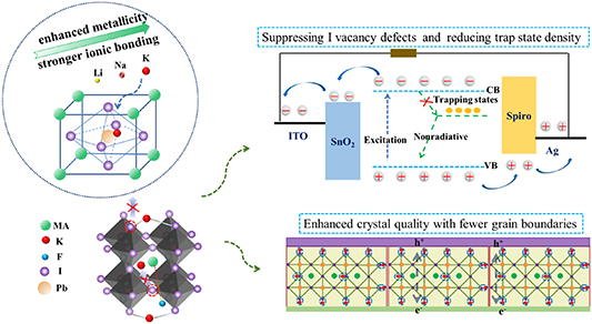
Based on the above results, the mechanism of KF passivating the defects in perovskite films is summarized in figure 8. As mentioned before, Li et al pointed out that the introduction of F− inhibits the dissociation and diffusion of organic cations, which can be attributed to the formation of hydrogen bonding between the fluoride and MA+ ions [15]. Meanwhile, these alkali metal ions are introduced in the perovskite films and form ionic bonds with halide anions, which effectively suppress the motion of I− and the formation of I vacancies. As a result, the trap state density is significantly reduced and the material degradation pathway is blocked. Among the three alkali metal ions, K+ exhibits the strongest ionic bonding with I− due to its highest metallicity, resulting in the best effect on passivating I vacancy defects. In addition, the existence of K+ also contributes to significant improvement in the growth and crystallization of perovskite film. The introduction of K+ leads to enlarged grain size with fewer GBs, which significantly reduces trap-assisted recombination centers, contributing to reduced carrier recombination and more efficient carrier transfer.
Figure 8. Schematic illustration of how KF realizes the promotion of photovoltaic performance of PSCs.
Download figure:
Standard image High-resolution image
4. Conclusion
In summary, we demonstrate an efficient perovskite passivation strategy by directly adding a certain amount of XF (X = Li, Na, K) into the perovskite precursor to improve the film quality and PSC device performance. With the addition of alkali metal ions, especially K+, perovskite films have better crystallinity with larger grain size and fewer GBs. Moreover, due to the formation of strong ionic bonding between K+ and I−, the I vacancy defects are effectively suppressed, contributing to the lower trap density and the longer charge-carrier lifetime. As a result, the enhancement of film quality leads to a great improvement in the device performance of PSCs. By optimizing the concentration of KF (1%), PSCs have finally achieved an enhanced PCE, as high as 20.11%, with significantly reduced hysteresis.
Acknowledgments
This work was supported by the National Natural Science Foundation of China (Nos. 61604131, 61704154 and 11804300), Natural Science Foundation of Zhejiang Province (No. LY19F040009), Fundamental Research Funds of Zhejiang Sci-Tech University (No. 2020Q039), National Undergraduate Training Program for Innovation (202010338031) and Xinmiao Undergraduate Student Talents Program of Zhejiang Province (2019R406018), Open Project of Key laboratory of Solar Energy Utilization & Energy Saving Technology of Zhejiang Province.
Data availability statement
All data that support the findings of this study are included within the article (and any supplementary files).
Author contributions
This manuscript was written with contributions from all the authors.
Conflict of interest
The authors declare no competing financial interest.