
Abstract
Low pressure single- or dual-frequency capacitively coupled radio frequency (RF) plasmas are frequently used for high-aspect ratio (HAR) dielectric etching due to their capability to generate vertical ion bombardment of the wafer at high energies. Electrons typically reach the wafer at low energies and with a wide angular distribution during the local sheath collapse. Thus, in contrast to positive ions, electrons cannot propagate deeply into HAR etch features and the bottom as well as the sidewalls of such trenches can charge up positively, while the mask charges negatively. This causes etch stops and distortion of profile shapes. Here, we investigate low pressure, high voltage capacitively coupled RF argon gas discharges by Particle-In-Cell/Monte Carlo collisions simulations and demonstrate that this problem can be solved by Voltage Waveform Tailoring, i.e. the velocity and angular distribution of electrons impacting on the electrodes can be tuned towards high velocities and small angles to the surface-normal, while keeping the energies of the impacting ions high. The applied voltage waveforms consist of a base frequency of 400 kHz with 10 kV amplitude and a series of higher harmonics. A high frequency component at 40 or 60 MHz is used additionally. Square voltage waveforms with different rise-times are examined as well. We show that high fluxes of electrons towards the wafer at normal velocities of up to 2.2 × 10⁷ m s−1 (corresponding to 1.4 keV energy) can be realized.
Export citation and abstract BibTeX RIS

Original content from this work may be used under the terms of the Creative Commons Attribution 4.0 license. Any further distribution of this work must maintain attribution to the author(s) and the title of the work, journal citation and DOI.
1. Introduction
In high-aspect ratio (HAR) plasma etching of dielectric substrates the flux and energy distribution of both the ions and electrons at the wafer greatly determine the rate and quality of the etch [1–6]. In typical low pressure single- or dual-frequency capacitive radio frequency (RF) discharges, the shape of these distribution functions is strongly different [7]. While positive ions are accelerated towards the wafer by the sheath electric field and hit it vertically and continuously with high energies, electrons reach the substrate during the local sheath collapse at low energies and with a wide angular distribution [8]. The etch process is driven by high energy ions and reactive radicals [9–16], but the fluxes of positive ions and electrons must balance at each surface element of a dielectric wafer locally on time average, including the bottom and the sidewalls of trenches [8, 17, 18]. In the presence of a wide angular distribution, electrons cannot penetrate deeply into HAR trenches. Consequently, the trench bottom and sidewalls can charge up positively due to the ion bombardment and further incoming ions are repelled from the corresponding surfaces. Thus, the ion flux is reduced locally to ensure the flux balance in the absence of electron fluxes to the corresponding surface element. As a consequence of this effect, etch stops and profile distortion due to ion acceleration towards the trench sidewalls can occur [18, 19]. Moreover, the mask can charge up negatively in the presence of a wide angular distribution of the electron velocities at the wafer. This can lead to an attraction of positive ions, which causes mask distortion [20, 21]. These issues represent significant limitations of modern HAR plasma etching and lead to a continuous increase of driving voltages to ensure even higher ion energies to overcome retarding potentials inside etch features.
This approach, however, only treats the symptoms of a problem, whose origin can be removed by ensuring in-feature surface charge neutralization. This requires the generation of a significant flux of electrons with high velocities directed normal to the electrode [20, 21]. This would also reduce the negative charge-up of the mask. One approach to realize a flux of directed high energy electrons into HAR features was proposed by Wang and Kushner [22]. They suggested to apply a dc (direct current) potential to the counter electrode. In this way ion induced secondary electrons are generated at the counter electrode and are accelerated towards the wafer by the dc sheath electric field. At low pressures, these energetic electrons will propagate through the plasma collisionlessly and arrive at the wafer at normal incidence. Thus, they can penetrate deeply into HAR etch trenches and neutralize positive wall charges. However, the flux of such secondary electrons is low due to their low emission probability and an unwanted dc current flows in the system. Alternatively, the plasma can be pulsed to extract negative ions, which can be accelerated towards the wafer by applying a bias potential in the afterglow [23], or neutral beam etching techniques can be used to avoid surface charging [24–26]. These technologies are relatively inefficient and expensive.
The ultimate solution to this problem requires a technique to tailor the entire electron velocity and angular distribution of the electrons in the direct vicinity to the wafer to generate a high flux of energetic electrons into etch features (similar to the positive ions). A promising concept to achieve this goal is Voltage Waveform Tailoring (VWT). Its ability to control plasma properties has already been demonstrated by simulations [27–34] and in laboratory experiments [35–37]. VWT was demonstrated to provide control of (i) the dc self-bias voltage via the Electrical Asymmetry Effect to improve the control of ion properties [8, 38–42], (ii) the sheath dynamics to control the electron power absorption dynamics and the electron energy distribution function [43–46], and (iii) nonlinear electromagnetic effects to optimize plasma uniformity [47–51]. Based on existing multi-frequency impedance matchings [52–54], VWT is a modular technology. Any existing capacitive RF plasma source can be upgraded to use VWT by modifying only the external circuit.
Recently, Krueger et al [33] reported that VWT could indeed be used to solve the problem of surface charging in HAR etch features. Based on Particle-In-Cell/Monte Carlo collisions (PIC/MCC) simulations of a low pressure capacitive RF plasma operated in argon, they demonstrated that an electric field reversal can be induced at the wafer during the local sheath collapse by tailoring the shape of the driving voltage waveform. By increasing the number of consecutive harmonics forming a peaks-type voltage waveform, the sheath collapse duration at the wafer was shortened. In this way the time, when electrons can compensate the ion flux at the wafer, is minimized. In order to draw enough electrons to the electrode to balance the ion flux on time average, a strong electric field reversal was found to be generated. Such field reversals strongly modify the velocity distribution of the electrons and their angular spread at the wafer, i.e. a high number of electrons hits the wafer at higher velocities and perpendicularly. In this way, electrons can penetrate deeply into HAR trenches to neutralize positive wall charges. Zhang et al [20, 21] used the velocity and angular distributions obtained in their work as input for a feature scale model and demonstrated that this technology indeed leads to surface charge neutralization inside HAR etch features and reduces mask distortion. This concept is similar to the effects of peaks- and valleys-waveforms in micro atmospheric pressure plasma jets [37, 55, 56] and is also similar to the effects of highly emissive boundary surfaces in dc plasmas [57, 58], which both lead to the generation of electric fields close to boundary surfaces that accelerate electrons towards this surface to balance the ion flux on time average.
While the work of Krueger et al [33] provided the fundamental concept of this new approach, it was not performed under conditions that are close to process parameters used in HAR dielectric plasma etching, because the driving voltage (1000 V) was too low, the fundamental driving frequency (5 MHz) was too high, and no interactions between plasma and typical surface materials used in HAR etching were included realistically. Therefore, in this work and in collaboration with Samsung Electronics Co., we study the potential of VWT to accelerate electrons to high velocities perpendicular to the wafer computationally at lower fundamental driving frequency of 400 kHz, higher low frequency voltage amplitudes of 10 kV, and including a realistic treatment of the interactions of the plasma with Si and SiO2 boundary surfaces in argon. To sustain the plasma a higher frequency of 40 or 60 MHz is added. These discharge conditions resemble those used in applications, while minimizing the complexity of the plasma chemistry. Using such a low base frequency has several technological advantages; higher voltage amplitudes can be applied without significantly altering the bulk plasma properties and the likelihood of more etch products to leave the trench within each period is increased. We study (1) the scenario, where multiple consecutive low frequency harmonics are combined with individually adjustable amplitudes and phases (peaks-type voltage waveform), as well as (2) square voltage waveforms with different rise- and fall-times. We reveal the fundamentals of the spatio-temporal ionization dynamics in such discharges and demonstrate that high electron fluxes at electron velocities perpendicular to the wafer of up to 2.2 × 10⁷ m s−1 (corresponding to 1.4 keV energy) can be realized, which is much higher as compared to that obtained previously [33].
The realistic implementation of plasma-surface interactions include energy and material dependent ion induced secondary electron emission (γ-electrons), electron induced secondary electron emission (δ-electrons), elastic electron reflection as well as inelastic backscattering of electrons. Previous studies demonstrated the importance of including such processes realistically [59–66] and also showed that using two different boundary surface materials at both electrodes can induce a plasma asymmetry [67–70]. Such surface material asymmetries often occur in actual plasma processes and are also studied in this work.
Investigations of capacitive RF discharges operated at such low fundamental frequencies and high voltages represent an extreme computational challenge due to the long fundamental RF periods and the extremely high energies of secondary electrons, which require using very short time steps. Therefore, we use GPU accelerated 1d3v PIC simulations complemented with Monte Carlo treatment of collision processes, which have previously been applied to study single- and dual-frequency discharges operated under similar conditions [70].
The paper is structured in the following way: in section 2, the simulation method is introduced. The results are presented in section 3, which is divided into two parts according to the different driving voltage waveform shapes studied in this work, i.e. peaks-waveforms (section 3.1) and square-waveforms (section 3.2). Finally, conclusions are drawn in section 4.
2. PIC/MCC simulation
We use a GPU accelerated 1d3v PIC/MCC simulation code to investigate the effects of different driving voltage waveforms on the velocity and angular distributions of the electrons at the wafer in low pressure capacitively coupled plasmas (CCPs) operated in argon. This code is described in details elsewhere [70], with further performance analysis and optimization strategies explained in [71]. Therefore, we only summarize the most important features of our code here.
The simulation corresponds to an electrostatic model that spatially resolves only the direction perpendicular to the electrodes but resolves all three dimensions in velocity space (1d3v). Electrons, Ar+ ions and Arf fast neutral atoms are traced. The collision processes of all the traced particle species include elastic, excitation and ionization channels [72–80]. The background gas temperature is calculated self-consistently, although no significant heating is observed under the conditions studied in this work. Secondary electron emission from the electrodes induced by all traced particle species, i.e. ions, fast neutrals and electrons, as well as elastic and inelastic reflection of electrons are included using impact energy dependent yields. Surface models for pure Si and SiO2 are implemented [63, 64, 81–87]. The corresponding secondary electron emission coefficients can be found in [70]. Note that these surface coefficients are typically higher for SiO2 compared to Si for the incident particle energies relevant to this work. Thus, more ionization can be present adjacent to a SiO2 compared to a Si electrode of identical surface areas. In this way, by using different electrode materials, a plasma asymmetry can be caused.
For diagnostic purposes we distinguish three groups of electrons. Bulk-electrons are created in the gas phase by ionization processes, while γ-electrons and δ-electrons are emitted from one of the electrodes by heavy particle (Ar+ or Arf) and electron induced electron emission, respectively.
One difference to our previous work [70] is the voltage waveform that is applied to the powered electrode located at x = 0, which is defined as:

where the first term,  , represents the tailored low frequency (lf) waveform defined in detail below for the multi-frequency and the square waveform separately. The base frequency of
  is fixed at 400 kHz for most of the cases studied in this work. For specific square waveforms it is varied from 200 to 800 kHz to study its effects on the energy and angular distribution of electrons at the wafer. The second term represents the harmonic high frequency (hf) component with frequency
  , amplitude
  , and phase angle
  . All these quantities are input parameters to the simulation, while the value of the dc self-bias voltage,
  , is determined during the simulation self-consistently based on the time averaged balance between the fluxes of positive and negative charges at each of the electrodes [88]. As this study is motivated by HAR etching application, we assume that the processing takes place at the powered electrode and, therefore, focus our efforts to optimize the conditions at this surface. The second electrode, located at x = L, is grounded. The combination of a voltage amplitude of up to 10 kV for the lf component and about 1 kV for the hf component is of high commercial interest for HAR plasma etching at low pressures. Under such conditions the lf component ensures high energy ion bombardment of the wafer and the hf component ensures strong electron power absorption required to sustain the plasma and to generate a high charged particle density. The electrode gap is kept constant at L = 5 cm. The neutral gas pressure (0.5–1 Pa) as well as the driving voltage amplitudes are varied. Due to the 1d spatial resolution, the discharge is geometrically symmetric in the simulation, i.e. the surface areas of the powered and grounded electrode are identical. Nevertheless, there are other sources of plasma asymmetry such as the shape of the driving voltage waveform and different surface coefficients of both electrodes, that correspond to different surface materials. These electrical and surface material asymmetries are captured by the simulation.
Simulation parameters were chosen to fulfill all numerical stability and accuracy criteria of the PIC/MCC scheme, as discussed in detail in [89]. An equidistant numerical grid with 1024 grid points was used for the computation of spatial distributions and for the solution of Poisson's equation, resulting in a spatial resolution of Δx ≈ 49 µm. The super-particle weight factor was set to obtain charged particle numbers in the range  for the converged solutions. A time-step of Δt ≈ 0.6 ps was used in the simulations, which was limited by the Courant–Friedrichs–Levy stability criterium due to the large applied voltages and thus the potentially very high electron velocities. Due to this small Δt, each low frequency cycle was divided into 4.17 million time-steps. Although convergence could be reached typically after a few hundred low frequency cycles, with a sequential implementation the execution times would reach several weeks. However, with our new GPU accelerated parallel implementation the run times could be kept as short as 1-3 days on Nvidia Pascal architecture.
The simulations yield the spatio-temporally resolved distribution of the potential, the electric field, the ionization rates due to different species and reactions, as well as the densities and fluxes of the charged particles. Important information is obtained, too, about the energy, velocity, and angular distributions of the electrons and ions impacting the electrode surfaces. Regarding the latter, our simulations yield the fluxes of the above species, resolved according to the velocity, the energy, or the angle of incidence. Although we call our results ion energy distribution function (IEDF), electron velocity distribution function (EVDF), and electron angular distribution function (EADF), it should be kept in mind that (1) these functions represent the fluxes of the given species resolved according to the respective quantity and (2) these distribution functions are different from those defined classically in kinetic theory.
3. Results
3.1. Waveforms synthesized from multiple harmonics
In principle, any periodic waveform can be constructed by adding a number of higher harmonics to a base sinusoidal wave, as known since the works of Joseph Fourier. In practice, there is always an upper limit for the feasible number of harmonics that one can apply, limited e.g. by the bandwidth of transmission lines or, as in the case of RF discharge technology, the availability of impedance matching units. In this section, the properties of low pressure high voltage argon CCPs driven by tailored voltage waveforms composed of a set of Fourier harmonics of a base frequency of  kHz are discussed. The emphasis is on the operational characteristics and the energy and velocity distributions of ions and electrons arriving at the electrodes. Building on the conclusions of earlier works [33], here we restrict ourselves to the 'peaks' excitation waveforms, because this provides a long and flat negative voltage base with a short and high amplitude positive peak, as illustrated in figure 1(a). This scenario is expected to favor the development of strong transient reversed electric field at the powered electrode during the local sheath collapse and, thus, the acceleration of electrons to the powered electrode. This is caused by the shortening of the local sheath collapse when using peaks-waveforms as compared to sinusoidal waveforms and the requirement of local compensation of electron and positive ion fluxes at each element of a dielectric surface exposed to the plasma.
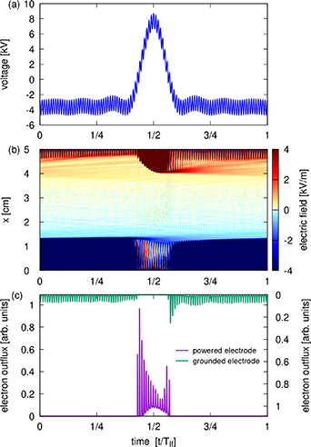
Figure 1. Time evolution of (a) the voltage at the powered electrode, (b) the electric field distribution, and (c) the electron flux arriving at the electrodes. In (c), the left scale corresponds to the powered electrode, while the right scale corresponds to the grounded electrode. Discharge conditions: p = 0.8 Pa, L = 5 cm,  kV,
kV,  kHz 'peaks' waveform with N = 7 harmonics, and
  MHz and
  V, identical electrode surface materials (SiO2 model).
  V.
V.
Download figure:
Standard image High-resolution imageThe peaks waveform is constructed using (1) with the voltage amplitudes Vk and phases θk of the harmonic components set according to [33]:
where N is the number of harmonics,  is the nominal low frequency voltage amplitude and
  is the low frequency base.
3.1.1. Identical electrode surface materials.
In this section, CCPs operated with both electrodes (powered and grounded) made of the same material (SiO2) are investigated.
Figure 1 shows the time evolution of Φ(t), the voltage at the powered electrode, the electric field distribution (with the data range restricted to small absolute field values), as well as the flux of electrons that arrive at the electrodes for a discharge operated in argon at 0.8 Pa,  kV,
kV,  kHz ('peaks' waveform with N = 7 harmonics),
  MHz and
  V. Φ(t) indicates the development of a high negative dc self-bias voltage of
  V as a consequence of the specific
  waveform. There is a clear correlation between the electric field that develops as a consequence of the applied voltage and the electron flux at the surfaces. During the phase of local low frequency sheath expansion no electrons can reach the adjacent electrode. At times of collapsed lf sheath the electron flux to the adjacent electrode is largely modulated by the high frequency sheath oscillation.
The observation that electrons can reach the surfaces only during the period of low frequency sheath collapse, and furthermore that, except for the γ-electrons, a simultaneous collapse of both the lf and hf sheaths is necessary for that, supports the concept that tailored voltage waveforms can be used to control the time within an lf cycle during which the electrons can reach the electrode and in this way the electric field reversal during the local sheath collapse. This field reversal is visible in figure 1(b) at the (bottom) powered electrode during the local simultaneous lf and hf sheath collapse as red regions.
Figure 2 shows the time averaged electron and Ar+ ion density and electric potential distributions. The only source of asymmetry introduced to the system in this case originates from the tailored voltage waveform, which is responsible for the formation of a significant dc self-bias voltage of  V due to its amplitude asymmetry [44] and a strong spatial asymmetry of the particle distributions. Even in the time averaged data, the difference of the nature of the RF sheaths adjacent to the powered and the grounded electrodes is evident. At the powered electrode the sheath is more extended and characterized by an almost complete electron depletion and a low ion density due to the large electric fields present. At the grounded side, the sheath region appears narrow and well populated by charged particles.

Figure 2. Time averaged spatial distributions of (a) the electron and Ar+ ion densities and (b) the electric potential. The discharge conditions are the same as for figure 1.
Download figure:
Standard image High-resolution imageIn order to gain deeper insights into the operation characteristics of CCPs under such conditions, figure 3 shows the time and space resolved ionization rate distribution and its decomposition into the contributions of all relevant particle species. Based on the time evolution we can identify the rising and the falling periods of  to trigger most of the ionization, with the falling section being more intense. Further, a strong high frequency modulation of the ionization rate can be observed suggesting the 'frequency coupling' effect to be a significant driving mechanism similar to dual-frequency CCPs [90]: a high amplitude of the lf+hf combined sheath expansion velocity is required in a region of reasonable plasma density to initiate sheath expansion heating efficiently. In the case of a fully expanded lf sheath, the hf modulation has a small amplitude, since it oscillates in a region of high plasma density, while during the fully collapsed lf sheath the electron density is too low. It is the phase during the lf sheath expansion when the hf oscillations provide optimal conditions for electron heating and for causing maximum ionization rates.
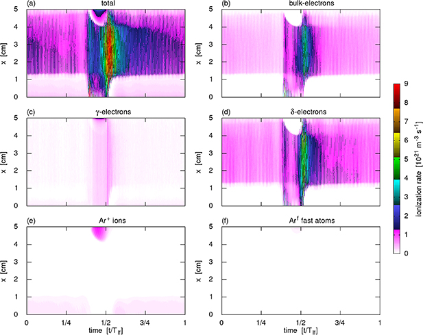
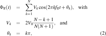
Figure 3. Spatio-temporal distribution of the ionization rate (a) and its decomposition into contributions of (b) bulk electrons, (c) γ-electrons, (d) δ-electrons, (e) Ar+ ions, and (f) fast neutral Ar atoms. The discharge conditions are the same as for figure 1.
Download figure:
Standard image High-resolution imageWith regards to the contributions of different particle species to the ionization, electrons play by far the largest role with 97.5% of the total charge production in the gas phase. It is, however, interesting to find that only 42% is caused by bulk electrons, while 49.5% of all ionization is induced by δ-electrons. These δ-electrons are emitted from one of the electrodes by energetic electron impact during a collapsed sheath period and are accelerated by the expanding sheath. γ-electrons contribute with 6%, Ar+ ions with 2.3% and Ar fast neutrals with only 0.2%. Despite the relatively small direct contribution of heavy particle collisions to the gas phase charge production it is to note that, based on the spatio-temporal distributions in figures 3(e) and (f), these new electrons are created deep inside the expanded electrode sheaths and, thus, are immediately accelerated into the bulk plasma and can reach significant energies. Figure 4 shows high resolution spatio-temporal plots of the electric field zoomed into the region of the collapsed low frequency sheath at the powered electrode for peaks waveforms composed of N = 3, 5, and 7 harmonics at otherwise identical discharge conditions as given in the caption of figure 1. In all cases, large amplitude oscillations driven by the high frequency voltage component dominate the field structure. Another prominent feature is the development of reversed electric fields (red color regions) during each hf sheath collapse phase. The duration of the collapsed lf sheath period narrows and with this the number of hf sheath oscillations within this time window decreases with increasing number of harmonics (N). As a result the electron flux to the powered electrode becomes more and more restricted in time and an increasing magnitude of the reversed electric field becomes necessary in order to ensure the overall flux balance. On the other hand, as quantified in the figure caption, the plasma density increases with increasing number of harmonics, which reduces the width of the expanded lf sheath, resulting in reduced sheath edge velocities during the hf sheath collapses. These two trends act against each other with respect to the reversed electric field formation. This can be tuned by varying
  , which is the most sensitive parameter influencing the plasma density.
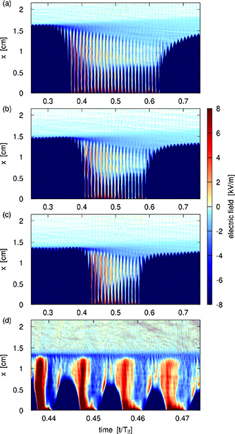
Figure 4. Spatio-temporal distribution of the electric field in the vicinity of the powered electrode at the center of the lf period applying (a) N = 3 harmonics, (b) N = 5 harmonics, and (c) N = 7 harmonics of the 400kHz base frequency to form the peaks waveform. Panel (d) shows a portion of the data from (c) with higher time resolution. The discharge conditions are the same as for figure 1. The dc self-bias voltages and mean electron densities are found to be:  V,
V,  V,
V,  V, and
  ,
,  ,
,  .
.
Download figure:
Standard image High-resolution imageThe effect of the number of harmonics on the ion energy and the surface-normal electron velocity and angular distributions (IEDF, EVDF, and EADF, respectively) at the powered electrode is shown in figure 5. The IEDFs indicate the presence of high energy ions, arriving at the electrode with several keV energy. The peak in the IEDF moves towards lower energies with increasing N. This is caused by the decrease of the absolute value of the minimum of the driving voltage waveform as a function of N. The time resolved voltage drop across the discharge, shown for N = 7 in figure 1(a), is the sum of the driving voltage waveform and the dc self-bias, which gets more negative as a function of N. However, the trend of the dc self-bias does not compensate the decrease of the absolute value of the minimum of the driving voltage waveform so that the maximum voltage drop across the sheath and, thus, the maximum ion energy at the powered electrode decrease as a function of N. The EVDFs show electron velocities up to  m s−1 (corresponding to about 180 eV energy). The shape of the EVDF shows little but systematic variation with N. The EADF reveals that the major fraction of the electrons arrives at the surface with incidence angles within a few degrees with a distribution slightly narrowing with increasing N. These results show that VWT allows to generate highly energetic electrons that propagate towards and perpendicular to the wafer, which can penetrate deeply into HAR etch features to neutralize positive surface charges inside such structures. Compared to other methods, a high number of electrons is accelerated in this way, since the field reversal affects all electrons located in vicinity of the wafer.

Figure 5. Energy distribution of Ar+ ions (a) and normal velocity and angular distributions of the electrons (b) impacting the powered electrode for peaks waveforms composed of N = 3, 5, and 7 harmonics. The discharge conditions are the same as for figure 4.
Download figure:
Standard image High-resolution image3.1.2. Different electrode surface materials.
It has been shown in [70] that using different surface materials for the powered and grounded electrodes introduces a significant asymmetry to the structure of the discharge and leads to the development of large dc self-bias voltages even for driving voltage waveforms that do not show any amplitude asymmetry. In the simulation, this situation is realized by applying different surface models (pure Si and SiO2 in our case) to the electrodes. This situation resembles conditions typically used for commercial plasma etching, where the electrode materials are typically different, i.e. the wafer/mask materials differ from those of the counter electrode and the reactor walls. It is expected that the amplitude asymmetry arising from the tailored voltage waveform can both enhance or reduce the effect of the surface asymmetry, depending on the electrode configuration.
Figure 6 shows a comparison of the two possible electrode configurations. The discharge parameters are given in the figure caption, in both cases a 'peaks' waveform composed of N = 7 harmonics of the  kHz base frequency is superposed with a
  MHz high frequency signal. The amplitude of the high frequency component is chosen individually for both configurations to result in similar peak electron densities in the bulk plasma to allow a direct comparison of the two configurations.

Figure 6. Spatio-temporal electric field distribution (a), (b), as well as IEDF (c), (d), EVDF and EADF (e), (f) at both the grounded and the powered electrodes for different electrode materials. In the left column the SiO2 and Si surface model is used for the powered (x = 0 cm) and grounded (x = L = 5 cm) electrode, respectively. The discharge parameters are: p = 0.8 Pa,  kV,
kV,  kHz 'peaks' waveform with N = 7 harmonics, and
  MHz with
  V. The dc self-bias is computed to be
  V. In the right column, the surface configuration is reversed. The discharge parameters are the same except for
  V, which is chosen to achieve comparable peak electron densities for both cases of about
  . The dc self-bias in this case is
  V.
V.
Download figure:
Standard image High-resolution imageIn the first configuration, shown in panels (a), (c) and (e) of figure 6 (powered electrode: SiO2, grounded electrode: Si) the electrical and the surface asymmetries act against each other resulting in comparable spatial extents of the two electrode sheaths and a low magnitude of the dc self-bias ( V). As a consequence, the IEDF, the EVDF and the EADF at the powered electrode have characteristics that are not in favor of the optimization goals of the present study. On the other hand, the characteristics of the reversed electrode material configuration (powered electrode: Si, grounded electrode: SiO2, figures 6(b), (d) and (f)) show the formation of a widely extended sheath and strong reversed electric field during the short and fast sheath collapse periods at the powered electrode. The dc self-bias voltage settles at a large negative value of
  V. As a consequence of the large potential difference between the bulk plasma and the powered electrode, the ions are accelerated to kinetic energies of approx. 6 keV during the long sheath expansion period. The electrons are also accelerated towards the electrode and reach velocities with a surface-normal component exceeding 107 m s−1, which corresponds to a kinetic energy of approx. 300 eV.
The asymmetry introduced by the second electrode material configuration, besides being potentially directly relevant to applications, provides an indirect way to emulate the effect of geometrical asymmetry that appears in real experimental systems. In industrial chambers, the powered electrode is typically significantly smaller compared to the total area of the electrically grounded surfaces, which results in the development of a significant negative dc self-bias voltage and a similar structural asymmetry as seen in figure 6(b). In commercial reactors, the geometric chamber asymmetry, the electrode material asymmetry as well as the amplitude asymmetry of the driving voltage waveform can be combined to generate an even stronger dc self-bias. This is expected to result in the generation of even stronger electric field reversals and even more energetic electrons at the wafer. A detailed study of this scenario is, however, beyond the scope of this work and would require 2d3v PIC/MCC simulations.
Observing the benefits of the second electrode configuration, in the following we will focus our discussion on this (powered electrode: Si, grounded electrode: SiO2) asymmetric system.
To illustrate the response of the discharge to the variation of certain discharge parameters, figure 7 shows the effect of a variation of  and of the number of harmonics N on the average plasma density and the maximum energy of ions arriving at the powered electrode. The plasma density is found to increase with decreasing
  and is mostly insensitive to the number of harmonics, in contrast to the findings for the symmetric surface material configuration, where the density shows clear correlation with N. The former dependence can be understood by taking into account that at such high voltage amplitudes and low gas pressures the electrons can easily get accelerated to energies well exceeding the regimes of the maximum probability for ionization and for secondary electron emission, both peaking in the few-hundred eV range. A reduction of the high
  increases the rate of electron energy relaxation into charge production channels. On the other hand, the maximum ion impact energy is proportional to
  but decreases with increasing number of harmonics. The latter effect, as already seen in figure 5, is a consequence of the dependence of the actual peak-to-peak voltage of the tailored waveform on the number of harmonics.

Figure 7. Mean electron density (a) and maximum Ar+ ion impact energy at the powered (Si) electrode (b) as function of the low frequency base voltage amplitude. Shown are results for a 'peaks' waveform composed from N = 3, 7, and 11 harmonics of the base frequency. The discharge parameters are: p = 0.8 Pa,  MHz and
  V.
V.
Download figure:
Standard image High-resolution imageThe IEDFs at the powered electrode, as shown in figure 8(a), reveal that besides the shift of the peak position to lower energies, the shape of the distribution remains mostly unchanged with decreasing  . This indicates that the low frequency voltage amplitude is a good external parameter that can be used to tune the energy of the impacting ions selectively.
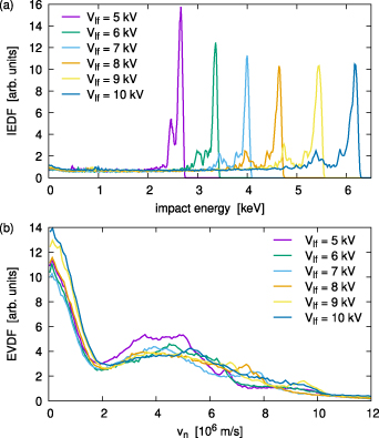
Figure 8. IEDF (a) and EVDF (b) at the powered electrode for 'peaks' voltage waveforms with N = 7 harmonics for different values of V . Discharge parameters are the same as in figure 7.
Download figure:
Standard image High-resolution imageAt the same time, the distribution of the surface-normal electron velocity, as presented in figure 8(b), shows little sensitivity on the low frequency voltage amplitude, with only a slight reordering towards higher velocities with increasing  .
.
The background gas pressure is another adjustable parameter that is available for process optimization in applications. Figure 9(a) shows that, at otherwise identical input parameters, the mean electron density rapidly drops with decreasing gas pressure below  Pa. The increasing electron mean free path clearly reduces the energy relaxation efficiency and ultimately prevents the formation of a stationary plasma state, as observed at pressures below 0.5 Pa. The plasma density stays fairly constant between 0.7 and 1.0 Pa. On the other hand, the maximum ion impact energy at the powered electrode is practically independent of the gas pressure showing variation only within 3% (see figure 9(b)).
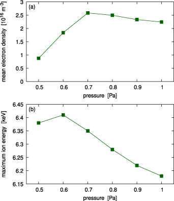
Figure 9. Mean electron density (a) and maximum Ar+ ion impact energy at the powered (Si) electrode (b) as a function of the argon gas pressure. Shown are results for a 'peaks' waveform composed of N = 7 harmonics of the base frequency. The discharge parameters are:  kV,
kV,  MHz, and
  V.
V.
Download figure:
Standard image High-resolution imageLooking into the details of the IEDFs and the EVDFs at the powered electrode with the help of figure 10 reveals that indeed the ion energy distribution is mostly invariant to the gas pressure, while the high velocity peak of the electron velocity distribution shifts significantly from  m s−1 at p = 1 Pa to
  m s−1 at p = 0.5 Pa. The effect of gas pressure on the EVDF is indirect, mediated by the spatial extent of the sheath region, which is in close relationship with the plasma density. In case of a wider electrode sheath at lower pressure, the bulk electrons have to travel a longer distance to reach the electrode. Therefore, a stronger reversed electric field has to develop to assist the sheath crossing.

Figure 10. IEDF (a) and EVDF (b) at the powered electrode for a 'peaks' voltage waveform with N = 7 harmonics, for different pressures. The discharge parameters are the same as in figure 9.
Download figure:
Standard image High-resolution image3.2. Square waveforms
An alternative to VWT by means of the multi-frequency synthesis is the application of pulsed signals or 'square waveforms'. In this section, operation details of high voltage, low pressure CCPs driven by combined low frequency square plus high frequency cosine voltage waveforms and possibilities of the control of the velocity and angular distributions of the electrons are discussed. Similar to the first approach, the lf component is meant to control the IEDF, while the hf component ensures the presence of strong electron power absorption to maintain a high density plasma.
Figure 11 illustrates the parametrization of the family of square voltage waveforms used in this section. The  low frequency signal is composed of two voltage plateaus with values
  and
and  (with
(with  kV in the present study), which are connected with linear voltage ramps as shown in figure 11(a). The
  rise-time denotes the duration of each voltage transition (the fall-time equals the rise-time). The ratio of
  , the time between the centers of the
  (rising edge) and the
  (falling edge) to the total period time (T = 2.5 µs in the present study) defines the duty cycle. A single
  MHz high frequency harmonic component with
  amplitude is superposed onto the low frequency waveform as shown in figure 11(b), and a self-consistently determined dc self-bias, which is kept constant during each low frequency period is added at last.
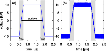
Figure 11. Schematic example of the 'square' waveform. The low frequency component,  , is characterized by the voltage amplitude
  , the rise-time
  , and the duty cycle =
  as illustrated in (a). Adding the
  MHz high frequency signal results in the waveform shown in (b).
Download figure:
Standard image High-resolution imageFigure 12 shows the evolution of the mean electron density as a function of the rise-time for a set of high frequency voltage amplitudes for both symmetric and asymmetric electrode material configurations. These results show that the qualitative behavior does not depend on the surface material symmetry. Therefore, we will focus on the asymmetric electrode configuration in the following as it has already been found to be advantageous with respect to the EVDF optimization at the powered electrode in the case of the peaks voltage waveform. Also apparent in figure 12 is the separation of operation into short ( ns) and long (
 ns) rise-time regimes showing opposite trends versus the rise-time variation suggesting very different electron power absorption mechanisms. In case of voltage waveforms with approximately 10 ns
  100 ns no stable discharge operation could be established. For this reason, further discussion is split into two branches.
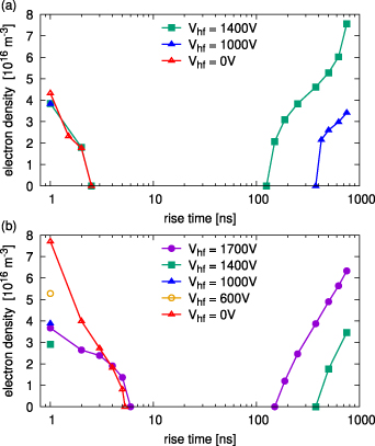
Figure 12. Time and space averaged electron density as a function of the rise-time,  , for a set of
  high frequency voltage amplitudes for (a) a symmetric SiO2 electrode configuration and (b) an asymmetric (powered: Si, grounded: SiO2) electrode configuration. The common discharge parameters are: p = 0.8 Pa, L = 5 cm,
  kV,
kV,  kHz, 50% duty cycle squares waveform, and
  MHz.
MHz.
Download figure:
Standard image High-resolution image3.2.1. Short rise-time square waveforms.
During the investigation of the operation characteristics of the short rise-time square waveform driven discharges, we limit the studies to the shortest reasonable rise-time, which is set to  ns, as we do not expect that experimentally any shorter high voltage switching would be practical.
In contrast to all cases studied above and in our preceding article [70], the short rise-time square voltage waveform is the only situation at which a stable discharge can be sustained without the need of a high frequency voltage component ( V) at such low gas pressure (p = 0.8 Pa) and high voltage amplitude (
 kV).
kV).
Figure 13 shows the spatio-temporal evolution of the total ionization rate and the electric field over the time period of a full low frequency cycle as well as sections around the voltage transition times with high resolution. From figure 13(a) we observe that the charge production is mostly confined into two short (≈ 100 ns long) time slices following the high voltage polarity transition. The applied square voltage waveform in this case has 50% duty cycle and, therefore, is symmetric in time. Nevertheless, the asymmetry induced by the different surface materials strongly affects the time evolution causing significantly different magnitudes of the ionization rates following the two transitions in favor of the falling edge direction. The high resolution details in figures 13(b) and (c) reveal the excitation of strong high frequency resonances of the electric field and, thus, the ionization rate enhancing effect of these oscillations. The frequency of the resonant oscillation excited by the rising edge transition is found to be 1.8 GHz. In case of the falling edge transition the response is more violent (and most of the charged particles are created near this time as indicated by the graph of the time dependence of the mean electron density, also shown in figure 13(a)). The resonance frequency is 1.5 GHz near the sheath edges, but the electric field structure becomes more complicated in the bulk region with significantly higher oscillation frequencies reaching up to 2.8 GHz. These GHz oscillations observed in the electric field coincide with equivalent oscillation patterns in the electron current distribution (not shown here). The observed frequency values and their trend with the plasma density are consistent with the plasma series resonance (PSR) phenomenon [91–96], where the excited electron plasma oscillation (defined by inertia) couples to the sheath capacitance resulting in the self-excitation of a resonance at a frequency of the order of  , where s and b are the length of the extended sheath and the bulk, respectively, and
  is the electron plasma frequency [97, 98]. The distributions of the ionization rate has a complex structure that exhibits (1) ionization maxima at the sheath edges modulated by the GHz oscillations and (2) beam-like features that propagate with constant velocity across the bulk and are reflected at the sheath edges and decay at longer time scales. The latter are generated by highly energetic electron beams via electron power absorption caused by the expanding hf sheath at the electrode, where the lf sheath is collapsed and the hf sheath, therefore, expands quickly in a region of low ion density.

Figure 13. Time resolved distributions of the total ionization rate and the electric field for a full low frequency cycle (a) and zoomed in to the  (b) and
  (c) transitions. In addition, the evolution of the mean electron density in (a) and the applied voltage in (b), (c) are displayed. The discharge conditions are: p = 0.8 Pa, L = 5 cm,
  kV,
kV,  kHz, 50% duty cycle squares waveform,
  ns,
ns,  V, and asymmetric (powered: Si, grounded: SiO2) electrode configuration.
Download figure:
Standard image High-resolution imageIncreasing the rise time makes the transition more gradual causing a smaller shock to the system resulting in a lower amplitude of the PSR oscillations and a slower lf sheath expansion. Assuming this mechanism to be responsible for the gas phase charge production, this trend is compatible with the observed rise time dependence of the plasma density shown in figure 12.
As the wavelength of the GHz oscillations is comparable, or even smaller than the size of typical plasma processing chambers, radial non-uniformity could be induced due to their self-excitation according to the non-linear standing wave effect [47, 50]. An accurate description of the spatial distribution of the plasma parameters would require higher dimensional and electromagnetic simulations, which is out of the scope of the present work.
The superposition of the  MHz high frequency component does not modify the principal operation mode of the discharge, nevertheless two important consequences of applying
  V are found. First, during the time of the low frequency sheath collapse, the high frequency voltage component induces large amplitude oscillations of the sheath edge causing alternating rapid collapse and expansion phases favoring the formation of electric field reversals, as shown in figure 4 for the peaks waveforms.
On the other hand, in cases where  the time of transition of the low frequency square waveform
  can be associated to a specific phase angle of the high frequency signal. The nominal high frequency phase is defined in (1) by the term
  . Figure 14 shows that in the case of
  V the choice of
  does strongly influence the mean electron density resulting in a ratio of 1.4 between the minimum and maximum values, while the dc self-bias (relevant for the shaping of the IEDFs) varies only within 1%. In the case of 50% duty cycle the
  transition of
  occurs in a short time period during which the actual phase of the high frequency cosine function propagates a few degrees around a center value
  . Due to the temporal symmetry of the applied waveform the phase of the high frequency signal during the falling edge transition is centered around
  . With the synchronization of the high frequency phase and the instance of the
  transition the magnitude of the actual sheath expansion can be controlled. If the transition happens during a fully collapsed high frequency sheath (
 in case of the powered electrode) the sheath expansion due to the high voltage transition is maximum, while in the case of an expanded high frequency sheath the displacement of the sheath edge is minimal. Figure 15 shows the high resolution ionization rate and electric field distributions for
  and
and  corresponding to the phases of maximum and minimum average electron densities respectively, as shown in figure 14.
Figure 14. Average electron density (a) and dc self-bias (b) as a function of the nominal phase angle of the high frequency voltage component. The discharge conditions are: p = 0.8 Pa, L = 5 cm,  kV,
kV,  kHz, 50% duty cycle squares waveform,
  ns, and
  MHz,
MHz,  V, asymmetric (powered: Si, grounded: SiO2) electrode configuration.
Download figure:
Standard image High-resolution image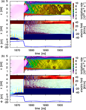
Figure 15. Time resolved distributions of the total ionization rate and the electric field for  (a) and
  (b) corresponding to the phases of maximum and minimum average electron densities, as shown in figure 14. The discharge conditions are: p = 0.8 Pa, L = 5 cm,
  kV,
kV,  kHz, 50% duty cycle squares waveform,
  ns,
ns,  V, and asymmetric (powered: Si, grounded: SiO2) electrode configuration.
Download figure:
Standard image High-resolution imageWith respect to the optimization of the IEDF and EVDF at the powered electrode, following our general strategy, the goal is to achieve an extended time period of the fully expanded sheath adjacent to the powered electrode interrupted by only short periods of sheath collapses. In order to achieve such a scenario the primary parameter of interest is the duty cycle and it is expected that with increasing  the rapid high frequency sheath motion during the
  period favors the development of strong field reversals.
Figure 16 shows IEDFs and EVDFs at the powered electrode for short rise-time ( ns) square waveforms for duty cycles varying from 30% down to 2% and
  V. The energy distributions of the impacting Ar+ ions are very pronounced uni-modal distributions, characteristic for high voltage collisionless sheaths. The position of the high energy peak shifts to lower energies as the duty cycle is decreased, since the dc self-bias gets more positive. For a duty cycle of 20% the dc self-bias is about −5700 V and increases to
  V for a duty cycle of 5% and even changes sign reaching
  V for a duty cycle of 2%.
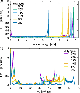
Figure 16. IEDF (a) and EVDF (b) at the powered electrode for short rise-time square waveforms with different duty cycles as labeled. The discharge conditions are: p = 0.8 Pa, L = 5 cm,  kV,
kV,  kHz,
kHz,  ns,
ns,  V, and asymmetric (powered: Si, grounded: SiO2) electrode configuration.
Download figure:
Standard image High-resolution imageThe distribution of the surface-normal velocity component of the impacting electrons shows an opposite trend with the dc self-bias, but here we have to distinguish different features and discuss their background separately to gain proper understanding. At the high velocity end a strong bi-modal peak represents the sole contribution of γ-electrons accelerated by the expanded sheath adjacent to the grounded electrode, which cross the discharge gap without losing energy in collisions. For this reason, their energy (velocity) is directly determined by the sheath voltage that further depends on the dc self-bias. Nevertheless, as in geometrically asymmetric experimental systems the sheath at the grounded side is expected to be significantly narrower with negligible potential drop, this population of electrons may not be present, and therefore is not in the focus of the present study. At the other end of the velocity spectrum the diffusional peak (at  ) is expected under 'usual' conditions in a single-frequency capacitively coupled RF discharge. However, under such extreme conditions this feature is populated mostly by δ-electrons that were emitted by electron impact secondary electron emission from the powered electrode and are guided back to the electrode by the reversed electric field experiencing no net energy gain. Our primary focus is on the formation of populations of electrons that are accelerated from the bulk plasma towards the electrode by a transient reversed field appearing as peaks at intermediate velocities in the EVDFs, usually in the range between 3 × 10⁶ m s−1
 m s−1 (corresponding to kinetic energies between 25 and 300 eV). In figure 16(b) a prominent peak in the EVDF is formed in the targeted velocity range showing increasing velocity with decreasing duty cycle. In addition to this spectral feature, already identified in the case of dual-frequency [70] and 'peaks' voltage waveform excitation (in section 3.1), a series of peaks appears at significantly higher velocities. The relative amplitudes of these high velocity peaks decreases with increasing duty cycle and vanish completely at approximately 20% duty cycle.
Figure 17 shows with high time resolution the electric field in the collapsing sheath region and the energy distribution of the electrons impacting the powered electrode during the short period of positive voltage phase of  for the square waveform with 2% duty cycle and 1 ns rise time. Right after the rising-edge voltage transition an extremely strong reversed electric field is formed accelerating electrons to energies up to 8 keV. The magnitude of this reversed field decreases to zero within the first 10 ns but is modulated by the GHz oscillations excited by the fast voltage rise. As a consequence the energy of the impacting electrons decreases with time, but each period of the GHz oscillation generates an enhancement of the energy distribution, ultimately causing the series of peaks in the time-averaged EVDFs, as seen in figure 16(b). With increasing duty cycle the magnitude of the initial reversed field decreases causing the reduction of this process, which fades at around 20% duty cycle as seen in figure 16(b).
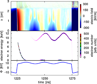
Figure 17. Distributions of the electric field and the energy of the electrons impacting the powered electrode as a function of time during the short positive voltage phase of  at 2% duty cycle. The panel in the bottom illustrates the applied voltage waveform, Φ(t). The discharge parameters are the same as in figure 16.
Download figure:
Standard image High-resolution imageAt later times within the low frequency voltage peak during each high frequency sheath collapse weaker field reversals are formed that accelerate electrons to a few 100 eV and are responsible for populating the first  peak in the EVDF. A third prominent feature in the middle panel of figure 17 is a 'wave' starting with some delay gradually after the first high frequency period. This feature corresponds to the γ-electrons that are emitted from the grounded electrode by ions that need time of about one high frequency cycle to gain enough energy from the expanded sheath at the grounded electrode to efficiently emit electrons. These γ-electrons are accelerated by the expanded sheath, cross the bulk plasma with low collision probability and arrive at the collapsed sheath at the powered electrode, which is modulated by
  . Therefore, the energy of the arriving γ-electrons is modulated, too, forming the bi-modal time-averaged EVDF seen in figure 16(b).
3.2.2. Long rise-time square waveforms.
The mode of operation of discharges driven with long rise-time square voltage waveforms is very similar to those driven with 'peaks' waveforms composed from harmonics of a base frequency. Charge production due to ionization collisions is most efficient at times during the low frequency sheath expansion when the superimposed high frequency sheath edge oscillation still has a large amplitude. In order to discuss the effect of different operation parameters on the charged particle distribution at the powered electrode we present results for an exemplary rise time of  ns, which defines the smallest possible duty cycle to be 10%.
Figure 18 shows the IEDFs and EVDFs for duty cycles of 10%, 30%, and 50%. The ion energy shows a unimodal distribution with a single large energy peak, typical for collisionless sheath conditions. The position of the peak shifts down with decreasing duty cycle, which directly reflects the variation of the dc self-bias voltage. As already seen in the cases of the 'peaks' and the fast rise-time square voltage waveforms, decreasing the time of low frequency sheath collapse, realized here with decreasing duty cycle, shifts the EVDFs to higher velocities. The underlying mechanism is as before: the charge fluxes to the electrode have to be balanced on time average and if the sheath is collapsed only for a small fraction of the RF period and the diffusion of the electrons is too slow, a reversed electric field forms to enhance the electron flux. As a consequence of this reversed electric field the electrons gain significant energy and impact the surface at close to normal angles.
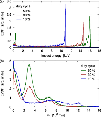
Figure 18. IEDF (a) and EVDF (b) at the powered electrode for different duty cycles of the long rise-time square waveform driven system. The discharge parameters are: p = 0.8 Pa, L = 5 cm,  kV,
kV,  kHz,
kHz,  ns,
ns,  MHz,
MHz,  V, and asymmetric (powered: Si, grounded: SiO2) electrode configuration.
Download figure:
Standard image High-resolution imageFigure 19 shows the IEDFs and EVDFs for different values of the low base frequency  , 400, and 800 kHz. We have chosen to keep the width of the positive voltage pulse equal for all three cases at the shortest possible value of 250 ns in the case of
  ns, resulting in values for the duty cycle to be 5%, 10%, and 20%, respectively. The observed shift of the peak position in the IEDF is caused by the different duty cycles through the variation of the dc self-bias voltage. As the ratio of the time duration of collapsed and extended low frequency sheath is smallest for
  kHz we expect the effect of the electron acceleration by the reversed electric field to be strongest here. Figure 19(b) confirms our assumption by showing the deformation of the broad high velocity peak towards higher velocities with decreasing
  . The EVDF extends up to
  m s−1, which correspond to energies up to 1.4 keV.
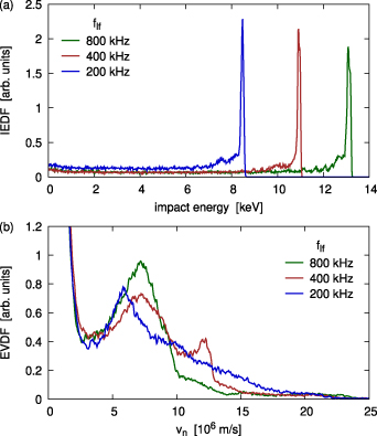
Figure 19. IEDF (a) and EVDF (b) at the powered electrode for different  of the long rise-time square waveform driven system. In all cases the pulse width was kept at 250 ns (corresponding to 10% duty cycle in the
  kHz base case). Other discharge parameters are the same as in figure 18.
Download figure:
Standard image High-resolution imageFigure 20 shows the IEDFs and EVDFs for different values of the low frequency voltage amplitude of  kV and 10 kV at
  kHz and 10% duty cycle. The peak position in the ion energy distribution is in direct proportion with
  , while the high velocity peak in the EVDF, which is populated mostly by bulk electrons that are accelerated to the electrode by a reversed electric field, shows much less sensitivity to
  in this range, as already seen for the peaks waveform.
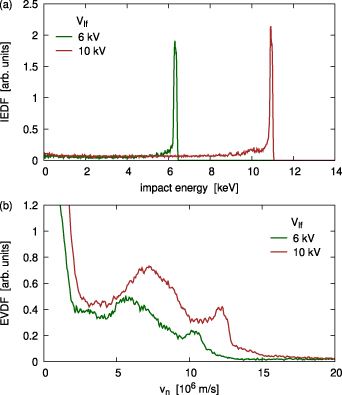
Figure 20. IEDF (a) and EVDF (b) at the powered electrode for different  voltage amplitudes at 10% duty cycle. Other discharge parameters are the same as in figure 18.
Download figure:
Standard image High-resolution image
4. Conclusions
In this study, the operation mechanism of low pressure, high voltage and low frequency capacitively coupled RF discharges, driven by two types of tailored voltage waveforms was presented. While keeping the plasma chemistry simple by considering argon plasmas, the operating conditions are relevant to HAR dielectric plasma etching.
Special emphasis was put on the distributions of the energy, the normal impact velocity, and the angle of incidence of the charged particles at the powered electrode, representing the wafer in HAR etching applications. Voltage waveforms constructed of harmonic components (Fourier synthesis) as well as pulsed ones (square waveform) were found to provide ideal conditions for the development of strong reversed electric fields during sheath collapse. Minimizing the total time of the collapsed sheath state can be achieved using higher number of harmonics or by using lower duty cycles, both resulting in the enhancement of the local electric field reversal. In the presence of short sheath collapses, such electric field reversals are required to accelerate electrons towards the electrode to balance the positive ion current on time average, because electron transport by diffusion is not sufficient. In case of square waveforms with very short rise times, the gas phase charge production is driven by strong resonances in the GHz frequency range excited by the fast high voltage transitions.
In this way, a high flux of energetic electrons into HAR features can be realized by VWT to minimize in-feature and mask surface charging that can result in profile distortion and/or etch rate reduction and stops. Compared to previous work [33] much higher electron velocities normal to the wafer of up to about 2.2 × 10⁷ m s−1 (corresponding to 1.4 keV energy) could be realized under process relevant discharge conditions. As VWT is a modular technique that allows each existing reactor to be upgraded by modifying only its external circuit, this technology could provide very significant benefits for plasma etching. Clearly, the effects of the driving voltage waveforms studied here on discharges operated in different, more complex gas mixtures should be investigated in the future and experimental tests should be performed.
Acknowledgments
This work is supported by the Samsung Electronics University R&D program [Control of electron distribution functions in dielectric plasma etching by voltage waveform tailoring to prevent surface charging inside etch features] and the China Scholarship Council (Grant No. 201906060024). Zoltán Donkó, Aranka Derzsi, and Peter Hartmann gratefully acknowledge financial support from the Hungarian Office for Research, Development and Innovation under NKFIH Grant Nos. K-134462, FK-128924 and K-132158. Thomas Mussenbrock gratefully acknowledges financial support from the German Research Foundation via MU 2332/6-1.
Data availability statement
The data that support the findings of this study are available upon reasonable request from the authors.