

Abstract
We have investigated the piezoelectric response of the hydrogenated graphene oxide (H-G-SiO2) stacks both experimentally and theoretically. The piezoresponse force microscopy method and density-functional theory (DFT) calculations were used to study the piezoresponse effect of this structure from both experimental and computational point of views. A mono-layer graphene, made by chemical vapour deposition method, is deposited on Si/SiO2 substrate and its surface is then functionalized with hydrogen atoms. The vertical piezoresponse, observed by piezoresponse force microscopy, is measured to be about 2146 pC N−1, that is comparable to the reported state of the art piezoelectric materials such as relaxor-based ferroelectric single crystals. In order to carry out the DFT modelling, a H-Graphene-O Janus structure has been adopted, where graphene is modified by oxygen atoms adsorbed on one side while hydrogen atoms are placed on the other side. Through modelling by DFT calculations, it is revealed that, by applying out-of-plane compressive uniaxial strain, the structure preforms different piezoelectric behaviours, up to three orders of magnitude alteration by the applied strain. The demonstrated approach for enhancing the piezo-response of graphene paves the way for realizing graphene-based nanoscale sensors, actuators and transducers.
Export citation and abstract BibTeX RIS
1. Introduction
Graphene is a mono-layer material in which carbon atoms are arranged in a hexagonal structure. Owing to their outstanding electrical, optical, mechanical and thermal characteristics, graphene oxide and hydrogenated graphene oxide, are believed to have great potential for applications in nanoelectromechanical systems, such as motors [1], sensors and actuators [2, 3], and robots [4]. However, due to its centro-symmetrical nature, graphene does not possess piezoelectric properties, which limits its application as a dynamic motion controller for the aforementioned applications. According to several recent theoretical and experimental reports, it is possible to break graphene inversion symmetry and induce piezoelectricity in graphene by chemical addition of adatom [5, 6], by introducing in-plane defects [7] or by applying engineered strain [8, 9], etc.
In this work, we have deposited a single layer graphene on Si/SiO2 substrate followed by functionalizing its surface with hydrogen atoms. The piezo-response is measured by means of piezoresponse force microscopy (PFM) and structural variations are investigated by Raman spectroscopy. The chemical functionalization has been confirmed by x-ray photoelectron spectroscopy (XPS) on CVD graphene on copper, after transferring onto Si/SiO2 substrate and after a hydrogenation step, respectively. The effects of both chemical interaction between SiO2 surface and graphene layer as well as the adsorption of hydrogen atoms on top surface of graphene (formation of a H-Graphene-O Janus structure) are deeply studied. An inhomogeneous interaction of graphene with SiO2 substrate, induces a biaxial in-plane strain which is observed in Raman spectroscopy, and increases the polarization of C–H bonds, in accordance with [6]. Therefore, the total measured piezo-response is attributed to the formation of out-of-plane polar C–O and C–H bonds. Furthermore, for comparison of the obtained results and investigating the governing physics behind this significant enhancement of piezo-behaviour, a thorough theoretical density functional theory (DFT) was carried out and the total piezoelectric effect created at the bottom and the top interfaces of graphene, was examined. Through theoretical modeling, the piezo response of the structure under both tensile and compressive strains was studied. The comparison of the experimental and theoretical results enlightened the effects of environmental and unwilling conditions on the experimental (H-C-SiO2) results, which may justify the smaller computed theoretical piezoelectric coefficients compared to the measured experimental ones.
2. Experimental approach
2.1. Sample preparation
Graphene was grown on a copper substrate in a horizontal quartz tube by chemical vapor deposition and then transferred onto a Si/SiO2 substrate by a wet process as outlined in [10]. The grown SiO2 has a thickness of 300 nm. The graphene is then hydrogenated using RF plasma in a hydrogen ambient. To perform the plasma hydrogenation, a parallel-plate reactive ion etching reactor operating at a frequency of 13.56 MHz was used. The samples are placed on the bottom electrodes with a diameter of 300 mm and to minimize the plasma reactivity and damages caused by energetic ions, hydrogen plasma treatment is performed at a low power of 13 W. During the process of plasma hydrogenation, the pressure of the chamber was 0.03 mbar and the gas flow was 200 SCCM (standard cubic per centimeter). To ensure about the saturation, nearly 30 min of hydrogen plasma treatment was required. When the graphene is incompletely hydrogenated, the material is called hydrogenated graphene rather than graphane. The hydrogenated graphene has reversible hydrogenation property, making it suitable for hydrogen based storage media [11]. To verify the reversibility of hydrogenation, we performed annealing of the samples in Ar atmosphere at 300 °C for 2 h. Confocal Raman microscopy is used to monitor the structural changes of graphene by hydrogenation and to study the induced strain to the hydrogenated graphene stack. Raman spectroscopy is carried out using a laser excitation with 532 nm wavelength. XPS was applied to analyze the chemical composition of the hydrogenated graphene oxide (HGO) stack and to examine the carbon oxygen and carbon hydrogen bonds. To extract data, a Gammadata-scienta ESC A200 hemispherical analyzer was used, equipped with an Al Kα (1486.6 eV) x-ray source. An Ntegra Prima AFM (NT-MDT) was used to perform the PFM measurements. The measurements were carried out by Pt-coated cantilevers obtained from NT-MDT: NSG10/Au (390 kHz resonance frequency, force constant 37.6 Nm−1) and CSG10/Au (39 kHz resonance frequency, force constant 0.5 Nm−1). In the contact mode, by CSG10/Au cantilevers, PFM and conductive AFM were performed. For the PFM measurements, practiced in a quasi-static regime, the frequencies were smaller than 100 kHz, and the a.c. excitation signal amplitude was ranging from 0 to 5 V. Also, The PFM amplitude was evaluated by the frequency-dependent measurements in the frequency range of 10–500 kHz.
3. First-principles calculations procedure
The numerical study of the H-C-SiO2 structure is performed using DFT. The computational modeling, is implemented using the Vienna ab initio simulation package (VASP) [12]. Generalized gradient approximation based on Perdew–Burke–Ernzerhof [13] along with a cutoff energy of 400 eV is employed. The charges distributed between graphene and SiO2 surfaces fluctuate and initiate Van der Waals interactions. To consider dispersion corrections caused by Van der Waals interactions, Grimme D2 method (DFT-D2) [14] is added to the modeling. Moreover, to prevent errors introduced by the periodic boundary conditions, dipole corrections are applied [15]. Consequently, the effect of finite size errors on potential and the forces and slow convergence of the total energy were minimized. To remove the interlayer interactions along the out-of-plane direction, a vacuum spacing twice the H-C-SiO2 stack thickness is assumed. The convergence criterion for relaxation is set to be smaller than 10–9 eV for the update of the total free energy between the successive iterations. The optimized structure in both the undistorted and under strain conditions are obtained by allowing ions, cell shape and cell volume to become relaxed, such that the acting forces on atoms becomes less than 0.02 eV Å−1. The polarization change as the result of strain exertion is estimated through Berry phase approach for the macroscopic electronic and ionic polarization, which is adapted for the application to ultra-soft Vanderbilt pseudopotentials and projector-augmented wave datasets describing the interaction between ions and electrons [16–18].
4. Results and discussion
4.1. Experimental measurements
Figure 1(a) illustrates the SEM image of the graphene sheet, transferred onto Si/SiO2 substrate while figure 1(b) displays the Raman spectra of the graphene for three cases including: (i) before, (ii) after exposure to hydrogen plasma and (iii) after annealing. These Raman spectra are normalized to achieve similar intensity for the G peak. Before hydrogenation, the characteristic Raman peaks are D, G and 2D at wavenumbers of 1353 cm−1, 1580 cm−1 and 2670.5 cm−1, respectively. In these spectra, D peak corresponds to the sp3 defects in the graphene lattice, G peak is attributed to the optical vibration of E2g phonons being at the center of the Brillouin zone, while 2D is originated by two phonon scattering process, being the sum of two phonons having opposite momentums [19].The ratio of I2D/IG, indicates that the transferred graphene is a single layer. By hydrogenation, sharp D and D' peaks appear at 1347 cm−1 and 1632 cm−1 wavenumbers, respectively. The 2D peak at 2669 cm−1 broadens slightly and its height decreases relative to that of the G peak (1583 cm−1). Moreover, a new peak (D + D') appears at about 2955 cm−1, which is the sum of two phonons having different momentums and dissimilar to the bands of the 2D and 2D', and its activation requires defect [19]. By annealing, all of the peaks (D, D' and D + D') related to the defect, were strongly suppressed and the peaks G and 2D (1581 cm−1 and 2669 cm−1), almost recovered to their original shape and position.
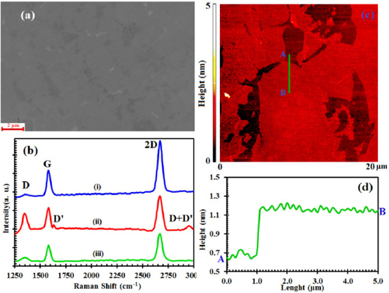
Figure 1. (a) The SEM image of transferred graphene on Si/SiO2 substrate, (b) Raman spectra of graphene on SiO2 (i) before, (ii) after exposure to hydrogen plasma and (iii) after annealing at 300 °C. (c) The AFM image of a graphene transferred on Si/SiO2 substrate. (d) Height profile of the AFM image.
Download figure:
Standard image High-resolution imageAs can be seen from figure 1(b(iii)), after annealing at a temperture of 300 °C, the ID/IG ratio significantly decreases. Previous studies show that the frequencies corresponding to G and 2D band peaks in graphene, shift with the applied uniaxial [20–22] and biaxial strain [23, 24]. Also  and
and  bands depend strongly on dopings, both electrically [25, 26] or chemically [27, 28]. Hence, to correctly estimate the strain, it is appropriate to separate the effects of the mechanical strain and the charge doping from the shift in the Raman peaks. To be able to do so, we use the correlation analysis between the two modes of graphene (
 ,
,  ) [29]. Typically, the compressive and tensile strains of the graphene lattice result into a phonon hardening (frequency upshift) and phonon softening, respectively. The shifts in the position of the peak caused by the exerted strain is the material intrinsic property and is quantified by Grüneisen parameters, describing the effect of volume modulation of a crystal lattice on the vibrational properties [30]. Since covalent bonds form in both X and Y directions, the Grüneisen parameter for biaxial strain
  is utilized in this work [29, 31, 32]. It is worth mentioning that for the phonons below 20 THz, Grüneisen parameter for graphene and hydrogenated-graphene are very similar [33, 34]. The magnitude of strain in a single layer graphene is given by
  , where
  is the Raman frequency in the absence of strain and doping and
  is the Raman frequency of the G band due to the strain (without the doping effect),
  is the strain based shift of the Raman frequency, and ε is the applied strain on the sample.
  of the G-band, where the strain and doping is assumed to be zero, is approximately 1582 cm−1 [29]. By using the correlation analysis used in [29], the values of the
  of the G band of the graphene/SiO2, hydrogenated graphene/SiO2 and annealed sample are equal to 1578 cm−1, 1575.7 cm−1 and 1576.5 cm−1, respectively.
By using strain equation  , an in-plane strain of 0.09% is obtained after hydrogenation of graphene on Si/SiO2 substrate. It is also worth noting that the values of strain before hydrogenation and after annealing are 0.06% and 0.08%, respectively. The topography measurements of the hydrogenated-graphene structure deposited on SiO2 substrate were implemented using a conventional tapping mode AFM (figure 1(c)) and its height profile is represented in figure 1(d).
To investigate the chemical modification of the CVD monolayer graphene, transferred on Si/SiO2 substrate and treated by hydrogen (H2) plasma, XPS is used. XPS is very appropriate tool to identify the chemical composition in carbonaceous samples [35–37]. The lorentzian-gaussian curve components were extracted by the deconvolution of XPS spectra at the different regions. Figure 2(a), shows the low-resolution XPS scan of the as-grown graphene film grown on Cu substrate, the graphene film transferred on Si/SiO2 substrate and the hydrogenated-graphene layer on the Si/SiO2 substrate.

Figure 2. (a) Low-resolution overall XPS scan of the pristine CVD graphene on copper (G/Cu), bare Si/SiO2 substrate (SiO2), graphene on Si/SiO2 substrate (G/SiO2) and hydrogenated graphene on Si/SiO2 substrate (HG/SiO2). High-resolution XPS scans for the: (b) C1s core level peak of G/Cu, (c) the C1s core level peak of G/SiO2, (d) C1s core level peak of HG/SiO2, (e) the Si2p peak of bare Si/SiO2 substrate and (f) the Si2p peak on Si/SiO2 substrate after transfer of graphene.
Download figure:
Standard image High-resolution imageFigure 2(b) depicts the high resolution XPS scan of the C1s for the graphene film grown on the Cu substrate. The peaks at 284.6 eV and 285.3 eV energies can be attributed to sp2-hybridized and sp3-hybridized carbon, respectively. The other four components of C–OH, C–O, C=O and COOH bnods are related to the peaks of 285.9 eV, 286.6 eV, 287.5 eV and 288.4 eV, respectively [36–38]. The presence of sp3 component in the deconvoluted spectra of C1s may be originated from the CH4 trapping or absorption, during the process of the CVD growth. Since the D band in the Raman spectrum of the figure 1(b(i)) is not strong, it is improbable that the C–H bonds are to be formed on as-grown CVD graphene [39]. The ratio of tetragonal to trigonal carbon bonds in graphene structure is given by ϴ/(1 + ϴ), in which ϴ is the ratio of sp3 to sp2-hybridized carbon component intensity [39].
The value of this ratio in the pristine CVD graphene is 0.09, so that the C–H/C–C bond ratio will be about 0.09/1.09 = 8.2%. About 13.2% of the total area of the C1s peak corresponds to the oxygen-related components resulting from decomposing the peak in the curve components, which might be the result of insufficient vacuum during the growth [37].
For the graphene, transferred onto the Si/SiO2 substrate (figure 2(c)), the C1s high-resolution XPS measurement depicts the peaks at the same energies of figure 2(b), that is at C sp2 with binding energy of (284.4 eV), C sp3 (285.1 eV), C–OH (285.8 eV), C–O (286.5 eV), C=O (287.0 eV), and COOH (288.5 eV), respectively. Upon transfer, the oxygen related components bonded with carbon are increased, from the original 13.2% to 22.3%. The enhanced sp3 components of the C1s peak (in comparison with the sp3 components of the C1s peak in figure 2(b)), corroborates the chemical configuration modification of the transferred layer due to possible bonding of carbon atoms with underlying oxygen atom from SiO2 substrate. The value of ϴ/(1 + ϴ) in figure 2(c), is about 18.9%. By deducing this quantity from its value obtained in figure 2(b), the oxygen coverage of graphene (C–O bond) is obtained to be about 10%. Using XPS, the hydrogen coverage on graphene has been evaluated. Figure 2(d) shows the C1s spectra of graphene transferred on Si/SiO2 substrate after hydrogenation (13 W, 0.03 mbar). The C1s spectra were fitted again with six components as same as the ones in figures 2(b) and (c) but it is worth mentioning that the ratio of the hybridized C components of the sp3/sp2 increases and the value of ϴ/(1 + ϴ) became 31.8%, which is an indication of the formation of C–H bonds. Using this value and comparing it with the previous values of this quantity, one can conclude that the hydrogen coverage of graphene is about 12.9%.
Figure 2(e) depicts Si2p peak corresponding to the bare Si/SiO2 substrate. As it can be seen, there is only one peak at 103.3 eV corresponding to the silicon oxygen bonding and it is consistent with literature [40, 41]. After transferring of graphene on Si/SiO2 substrate (figure 2(f)), a week shoulder toward the lower binding energies of the main Si2p peak is observed, causing a new peak after deconvolution. The intensity of this peak is weaker and we speculate this to be due to a Si–O–C bonding which is another evidence of C–O bonding [42]. The intensity ratio of Si–O–C bond to Si2p peak is about 10% which was extracted from the graphene C1s peak.
To detect tiny vibrations of graphene surface between the tip and the substrate, an a.c. voltage of 5 V at a frequency of 90 kHz is applied. Measurements are performed in the contact mode. The piezo-response has negative sign and the induced amplitude of vibrations is about 0.04–0.05 nm (figure 3(a)). To detect PFM signals, a voltage spectroscopy measurement is performed in the step mode on the graphene, GO and on hydrogenated graphene oxide stack, HGO. For this purpose, between the tip and the substrate, an a.c. voltage of about 1 V at a frequency of 20 kHz is applied. By sweeping the d.c. bias from −10 V to 10 V, the piezoresponse on HGO stack and graphene oxide (GO) stack (before hydrogenation) was studied (figure 3(b)). The strain along the out-of-plane direction is modeled by considering the initial thickness of the layer L as:  , where
  is displacement of the atomic position extracted experimentally by PFM along the out-of-plane direction (at quasi static regime with a frequency of 20 kHz and a displacement amplitude of about 0.02 nm (see figure 3(b)).
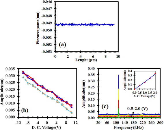
Figure 3. (a) The piezo-response on pure graphene structure, (b) piezo-response amplitude versus d.c. voltage measured in the step mode on HGO stack (circles) and on GO stack (triangles), (c) PFM amplitude dependency at different ac voltage to the frequency at the cantilever fundamental resonance measured on HGO layer. Inset: PFM amplitude at the resonance versus applied ac voltage.
Download figure:
Standard image High-resolution imageThe amplitude of piezo-response increases for the applied negative d.c. voltages and it decreases for positive d.c. voltages. By applying a negative electric field to the tip, C–O and C–H dipoles, become closer to the vertical direction and hence the net polarization increases. By applying a positive electric field to the tip, dipoles will get away from vertical direction so that the net polarization decreases [8]. No hysteresis is observed, because the orientation of the fixed dipoles cannot be altered by any external electric field. To study the linearity and the piezo-electric nature of the response, the signal dependency to the frequency under various a.c. voltages is investigated. Figure 3(c) shows the amplitude of PFM signal versus different a.c. voltages at the cantilever fundamental resonance. The cantilever on graphene (HGO) resonates at a frequency of about 112 kHz. The inset of figure 3(c) shows the linear behaviour of amplitude versus a.c. voltage up to 2 V, which demonstrates the piezoelectricity of HGO layer (since no hysteresis is observed).
The governing physics interpreting the piezoelectric response of the hydrogenated graphene oxide is that by transferring the graphene layer onto SiO2/Si substrates, carbon atoms of graphene interacts chemically with the terminated oxygen atoms of SiO2, and C–O bonds are formed. Because of the electronegativity of oxygen, C–O bonds are polar and a net dipole moment in the system forms which in turn induces an anisotropic strain. By functionalizing the surface of graphene with hydrogen atoms, C–H bonds are formed with free carbon atoms of graphene that did not interact with oxygen atoms.
According to [6], if graphene is doped with adatoms like hydrogen, exerting an equi-biaxial in-plane strain to graphene induces a change in the polarization and increases the polarization of C–H bonds and the net polarization increases (in this case, hydrogenated graphene oxide, HGO). By applying an electric field with the aids of the AFM tip, the C–O and C–H dipoles re-orient to become closer to the normal direction and a PFM signal is detected.
Based on the mirror charge method calculations to obtain the electric field 'E', in the carbon oxide layer, the average uniform electric field in the hydrogenated graphene oxide layer below the tip is (supplementary information of [8]):
where  is the SiO2 dielectric constant [43] and according to our simulations (refer to supplementary information (stacks.iop.org/JPhysD/53/175303/mmedia)), the dielectric constant of hydrogenated graphene oxide stack is
  . In equation (1), the applied voltage on the tip is
  and
and  is the radius of the AFM tip. The higher value of the dielectric constant in HGO structure compared to that of GO could be explained by extra bond between C and H in HGO that permits electrons to polarize along the bond more freely than in GO. This is in agreement with the numerical results as will be shown later, an increase of the polarizability is expected.
To obtain the piezoelectric coefficient d33, by using the vertical strain induced by the intrinsic ( ) and the inductive (
 ) polarizations in the presence of direct and alternating external electric fields, we derive the displacement amplitude normal to the surface detected by the PFM and calculate the result using the measured data. Induced strain can be written as

where  . By casting this relation in equation (2) and excluding the electrostatic term (
 ) and by using
  :
:

The applied electric field consists of direct  and alternating
  components. By insertion of these components into equation (3) and discarding static terms (
 ) and leaving only first order components depending on the electric field
  , the equation (3) will be:

Considering the alternating electric field in the form of  , vertical to the surface displacement being detected by PFM, is expressed in the form of
  , and it is related to the vertical strain as
  which
which  is the thickness of hydrogenated graphene oxide layer (HGO). So the first harmonic amplitude can be obtained as;

Assuming  , it leads to
  , and by entering the electric field from equation (1), which is now only an alternating field, the longitudinal piezoelectric coefficient takes the form,
where  is the amplitude of the first harmonic and the magnitude of a.c. electric component (Ea.c.) is E0. The thickness of hydrogenated graphene oxide layer is
  (the bonding length of carbon–hydrogen bond is about 1.09 Å [44] and for carbon-oxygen bond is about 1.2–1.5 Å [45]). At low frequencies (~20 KHz), the values
  are obtained from figure 3(c), at zero d.c. bias for HGO and GO stacks, respectively. By substituting these values in equation (6), the piezo-electric coefficients are obtained as
  , respectively, which are about two times higher than the value obtained for the graphene transferred onto the Si/SiO2 substrate (GO stack) and about × 1.5 the
  value reported for graphene on SiO2 grating substrate. This value are significantly larger than piezo-electric ceramics of the lead zirconate titanate family.
4.2. Piezo-electric modelling
In this section, the results of our computational modelling for the piezoelectric behaviour of the H-C-SiO2 structure is discussed. The piezoelectric effect enhancement, resulting from the co-adsorption of oxygen atoms on a monolayer graphene is first investigated. In the hydrogen/graphene/SiO2 structure, hydrogen atoms are assumed to be adsorbed on the surface of the graphene sheet, while oxygen atoms of SiO2 surface are adsorbed on the other side to form a H-Graphene-O Janus structure. The side and top views of the atomistic configuration of H-C-SiO2 are shown in figure 4, where x, y , and z are denoted as the zigzag, armchair and out-of-plane directions of the graphene layer, respectively. The optimum H-C-SiO2 structure with the least total energy is determined by choosing a supercell as can be seen in figures 4(a) and (d) with the lattice constants of a = 4.53 Å and b = 5.12 Å along the X and Y directions. To model the structure as a quasi-2D martial, the out-of-plane lattice constant is equal to c = 49.43 Å, being more than twice the thickness of the structure which is 22.24 Å.
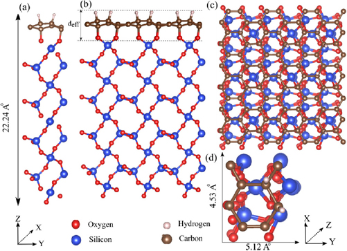
Figure 4. The hydrogen/graphene/SiO2 structure. Blue, white, red and brown circles are Si, H, O and C atoms, respectively. (a) The side view of each unit cell, (b) and (c) are the extension of the unit cell along the X and Y directions and (d) is the top view of the unit cell.
Download figure:
Standard image High-resolution imageNow, to evaluate the piezoelectric behavior of the structure, the piezoelectric coefficients are calculated. The piezoelectric coefficients are generally described by the full third-rank piezoelectric tensors as  and
and  . Due to the crystal symmetry, in the Voigt notation, the mentioned third-rank tensors are reduced to
  and
and  tensors, with l = 1..., 6. Accordingly,
  and
and  as vertical tensors are defined as:
where,  ,
,  ,
,  and
and  denote surface polarization, strain, stress and macroscopic electric fields along the out-of-plane direction, respectively. To calculate the piezoelectric coefficients
  and
and  , it is necessary to compare the developing dipole moments originated by the exertion of the strain along the out-of-plane uniaxial direction from the initial polarization moment of the undistorted structure (the unstrained relaxed structure with the minimum total energy). Using Berry phase expressions implemented in VASP, the total contribution of the ionic and electronic dipole moments change due to the strain are calculated [16–18]
Then the obtained dipole moment through a volume consisting of the unit cell area and a specific effective thickness (deff) as shown in figure 4(a), is turned into the three dimensional (3D) polarization in which the distortion of ions effectively gives rise to polarization modulation.
The compressive and tensile strains are modeled by lowering and heightening the upper hydrogen atoms to a fixed out of plane atomic coordinate respectively, while; the atomic positions of the structure are allowed to relax in all directions. Appling an array of out-of-plane strains from −4% (compressive strain) to +4% (tensile strain) on the H/C/SiO2 structure shown in figure 4(a), reveals that lower oxygen atoms closest to the graphene layer are the only ions of SiO2 substrate being distorted by the initial strain (next group of oxygen atoms stayed undistorted), thereby the polarization change is mostly originated from the distortion of the relaxed ions along the distance between the upper hydrogen and lowermost oxygen atoms closest to the graphene layer. This distance is denoted as the effective distance  being equal to 3.214 Å for the undistorted condition. Therefore, the effective strain as a post relaxation computation is obtained by
  , in which
  is the amount of effective thickness modulation and the
  is the undistorted effective thickness.
Finally, the stress corresponding to each exerted strain is computed. So, under an out-of-plane strain, in addition to the ionic relaxation, the volume and shape of the unit cell are first relaxed. For a precise evaluation, the lattice vector along the z-direction is fixed, whereas the length of lattice vectors along the x and y directions are altered iteratively, so that the in-plane stress becomes smaller than 10–4 Gpa. Then the sum of the forces on the hydrogen atoms is extracted as the uniaxial out-of-plane force exerted on the unit cell corresponding to each strain.
To compute the piezoelectric coefficients e33 in equation (7), it is required to evaluate 3D polarization modulations  under an array of exerting strains. Figure 5, depicts the extracted 3D polarization modulation versus the applied compressive and tensile strains computed by the presented DFT procedure. As can be seen in figure 5, the H-C-SiO2 structure performs two different piezoelectric responses for small and large values of strain. Also it can be seen that under smaller strains from −0.025 of compressive to 0.015 of tensile strains, the 3D polarization modulation is less than its piezoelectric response for larger strains. It can be indicated that the piezoelectric behavior of the structure largely depends on the distortion of the symmetric configuration of the structure. Due to the rigid chemical bonding between graphene layer and the hydrogen and oxygen atoms, by small out-of-plane strains, the symmetric structural configuration is retained more than the large exerted strains. Consequently, the modulation of ionic dipole and electronic moments resulting from the small displacement of the ions would not be as much as large strains.
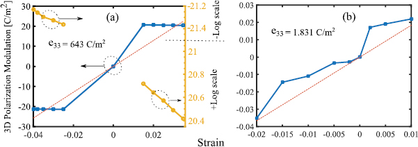
Figure 5. (a) and (b) 3D polarization modulation variations versus compressive out-of-plane strain, piezoelectric coefficient and (e33) versus compressive vertical strain.
Download figure:
Standard image High-resolution imageFurthermore, the abrupt rise of polarization modulation at the 0.015 tensile strains compared to the −0.025 compressive strains can be seen in figures 5 and 6 which can be attributed to higher sensitivity of the H-C-SiO2 material to tensile strains. On the other side, as can be seen in figure 5, further increase of tensile and compressive strains more than 0.015 and −0.025, decreases the polarization modulation. This contrary behavior is correlated to the decrease of ionic and electronic dipole moment modulations resulting from the electronic transition of the H-C-SiO2 material under an out-of-plane strain. As both the compressive and tensile strains are increased, the bandgap of the graphene layer narrows more and finally, a semiconductor to metal phase transition occurs. The bandgap of a buckled 2D material decreases with the exertion of an out-of-plane compressive uniaxial strain. Due to the co-adsorption of hydrogen and oxygen at the surface of graphene, the layer is buckled enough, being subject to semiconductor to metal phase transition under the mentioned strain.
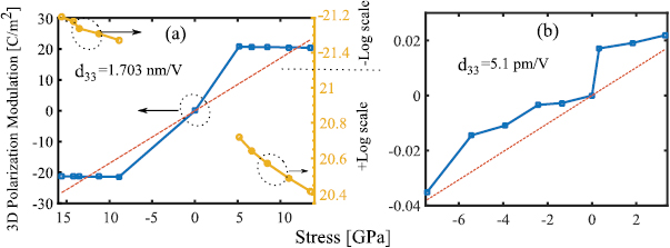
Figure 6. (a) and (b) 3D polarization modulation variations versus compressive out-of-plane stress, piezoelectric coefficient (d33) versus compressive vertical stress.
Download figure:
Standard image High-resolution image
For the evaluation of piezoelectric coefficients d33 by the equation (8), 3D polarization modulation  under the out-of-plane stress must be extracted. As explained before, the stress corresponding to each strain can be computed. Figures 6(a) and (b) show the 3D polarization changes versus stress for both small and larger values of stress. Now by using 3D polarization modulations under the exerted strains and their corresponding stresses, one can calculate the
  and
and  as shown in figures 5(a), (b) and 6(a), (b). The slopes of 3D polarization modulation plots versus strain and versus stress in figures 5 and 6(a), (b) are denoted as e33 and
  , respectively. Due to the different piezoelectric response of the structure for different strain values, two different
  and
and  coefficients as 643 C m−2 and 1.831 C m−2 and 1.7 nm V−1 and 5.1 pm V−1 were computed for small and large strain regimes, respectively.
To compare the results of the theoretical modeling with the experimental physical findings, the  and
and  coefficients were computed by differentiating the distorted (strained) polarization with the undistorted (unstrained) condition for each applied strain. The computed results for some of the small and large strains are collected in table 1.
Table 1. Piezoelectric coefficients d33 and e33.
| Strain [%] | Stress [GPa] |  (C m−2) (C m−2) |
 (nm V−1) (nm V−1) |
|---|---|---|---|
| −0.04 | −15.5 | 530 | 1.36 |
| −0.035 | −13.5 | 608 | 1.57 |
| −0.025 | −8.85 | 854 | 2.4 |
| −0.02 | −7.43 | 1.7 | 4.7 × 10⁻³ |
| 0.005 | 1.82 | 3.82 | 1 × 10⁻³ |
| 0.01 | 3.28 | 2.19 | 6.7 × 10⁻³ |
| 0.015 | 5.15 | 1381 | 4.02 |
| 0.025 | 8.46 | 822 | 2.43 |
| 0.035 | 13.4 | 583 | 1.51 |
Our procedure to relax the H-O-SiO2 (assuming crystalline SiO2) as can be seen in the figure 4, reveals the presence of C–O and C–H bonds. This is consistent with the XPS experimental measurements as shown in figure 2. The theoretical and experimental results extracted in this work are compared with some other works in table 2. As seen in table 2, the extracted theoretical result for  is close to that of the experimental one in this work. Both show the same order of magnitudes in the range of a few nm V−1 with about 0.7 nm V−1 deviation. This difference might be attributed to some usual non-idealities in the experimental materials, procedure and the environmental conditions. For instance, for the DFT calculations we assumed a crystalline SiO2 and the graphene layer with no defects or impurity. Also to model a quasi-2D structure a vacuum space was assumed on the upper area of the 2D structure, while in the experimental work, such condition is not met and the measurement is performed in an air ambient.
Table 2. Piezoelectric coefficients of some reported 2D structures.
| Structures |  (C m−2) (theoretical) (C m−2) (theoretical) |
 (pm V−1) (theoretical) (pm V−1) (theoretical) |
 (pm V−1) (experimental) (pm V−1) (experimental) |
|---|---|---|---|
| This work (H-Si-SiO2) | 643, 1.831 | 1703, 5.1 | 2146 |
| Graphene on SiO2 [8] | — | — | 1400 |
| PZN-8%PT [47] | — | — | 2500 |
| PbTiO3 single crystal [48] | — | — | 143 |
| MoSSe, MoSeTe, MoSTe, WSSe, WSeTe, WSTe [43] | 0.352, 0.428, 0.835, 0.294, 0.374, 0.752 | 5.248, 6.217, 10.575, 5.319, 6.710, 9.279 |
According to table 2, both the extracted theoretical and experimental results reveal that the studied structure performs a significant piezoelectric behavior comparable to best bulk piezo-layers such as polycrystalline materials and single crystals of relaxor perovskite.
Table 2, also shows the calculated out-of-plane piezoelectric coefficients of mono and few layers MXY (M = Mo or W, X/Y = S, Se, or Te) as an uttermost recent theoretical study [46]. The structure studied in this work possesses piezoelectric coefficients that are almost three orders of magnitude larger than that of MXY structures under large values of strain. Even under small values of strain, the studied H-C-SiO2 structure exhibits piezoelectric coefficients comparable to that of MXY structures.
Such a high piezoelectric response of our structure compared to MXY in [46] is attributed to the higher efficacy of different types of oxygen and hydrogen ions for the increment of dipole moments. It is similar to the enhancement of the piezoelectric response which has been reported in the [8]. In [8] the graphene layer on the SiO2 substrate has the  equal to 1.4 nm V−1. On the other hand in [17] it is shown, that the pristine graphene and the circular porous graphene nanoribbon does not exhibit any piezoelectric behavior, while graphene sheets containing triangular holes have a piezoelectric coefficient of about 0.124 C m−2. Compared to our structure, the studies depict that the co-adsorption of different ionic atoms on the graphene sheet is more effective and an easier approach than an arbitrary intentional alteration of the structure to bring sufficient dipole moment modulations. For example, the work presented in [49] depicts that clamped-ion and relaxed-ion of 2D transition metal dichalcogenides (TMDCs) benefit from the 2D in-plane d11 piezoelectric coefficient from 0.60 pm V−1 to 4.60 pm V−1. Although compared to [49], our structure may benefit from the higher piezoelectric coefficients. More investigation on the out-of-plane piezoelectric coefficients of clamped-ion and relaxed-ion of 2D TMDCs is required to fairly compare the structures.
5. Conclusions
In summary, we have observed a significant enhancement of piezo-electric response of hydrogenated graphene on Si/SiO2 substrates. The experimental and theoretical studies on the hydrogenated graphene oxide stack using piezo-response force microscopy and calculations based on density-functional theory (DFT) are reported. Vertical piezo-response, observed by piezo-response force microscopy, is about 2146 pC N−1, which is 1.5 folds larger than the  value reported for graphene on SiO2 substrate and comparable to that of the piezo-electric ceramics of the lead zirconate titanate family. The DFT calculations on electronic structure of graphene, modified chemically by oxygen adsorbed on one side and hydrogen adsorbed on the other side show that, by out-of-plane compressive uniaxial strain, the structure has different piezoelectric behaviours, such that its piezoelectric coefficients change three orders of magnitudes by the increase of strain. The demonstrated approach for enhancing the piezo-response of graphene paves the way for realizing graphene-based nanoscale sensors, actuators and transducers.
Acknowledgments
This work has been partially supported by Iran National Science Foundation (INSF).