

Abstract
We have investigated Ge nanowire (NW) metal–semiconductor–metal (MSM) photodetectors with high specific detectivity and low dark current, in which various sizes Ge NWs were fabricated by three-dimensional (3D) Ge condensation techniques. It has been demonstrated that the photocurrent gain increases significantly from 6.31 × 10⁴ to 4.47 × 10⁶ with the reduction of Ge NW width from 170 to 35 nm. A low dark current of 5.1 nA and an ultra-high specific detectivity of 1.26 × 1014 cm·Hz1/2·W−1 at 560 nm under 0.51 V bias are achieved for the 35 nm wide Ge NW photodetector. It has been proposed that the interface states provided by SiGeOx formed during Ge condensation process serve as electron traps to generate photogating effect, resulting in high photocurrent gain and high specific detectivity in the MSM photodetector. The fully complementary metal-oxide-semiconductor (CMOS) compatible and scalable process suggests a great potential of the Ge NW for low cost, high performance near infrared photodetectors.
Export citation and abstract BibTeX RIS
1. Introduction
Semiconductor materials and some organic materials are widely used in the preparation of sensors and memories due to their special material structures [1–8]. 1D semiconductors, such as nanowires (NWs), have attracted considerable attention because of their superior mechanical, electrical, and optical properties that are different from those of their bulk material counterparts [9–13]. It is widely accepted by research community that metal–semiconductor–metal (MSM) photodetectors based on bulk semiconductors have no gain in terms of quantum efficiency. The photocurrent gain can be obtained only in avalanche photodiodes, phototransistors or photoconductors based on avalanche multiple effect, amplification or so-called 'recycling gain mechanism'. Recently, Dan et al [14] reported that photoconductor intrinsically has no gain or at least no high gain and the gain should be the photogenerated excess carriers non-uniform distribution in the cond uctors with extrinsic effects, such as defects, surface states et al. In this viewpoint, ultra-high photocurrent gain from NW photodetector can be well understood with a large ratio of surface area to volume. In fact, Ge NW photoconductors with high photocurrent gain has been reported by several groups [15–18]. Raychaudhuri et al has reported a single Ge NW-based photodetector, which showed an enhanced responsivity (~107 A W−1) in the wavelength range of 300–1100 nm [16]. Ray et al used single GeO2–Ge NW to make photoconductor, also showing an enhanced responsivity of ~103 A W−1 and detectivity of ~1012 Jones, respectively, in the wavelength range of 350–900 nm [19]. Most of Ge NWs they used for photodetector were grown by a vapor phase method using gold (Au) nanoparticle (NP) as the catalyst dispersed on a silicon substrate [20–22]. However, it is difficult to control the size, crystal quality, and position of Ge NW. In addition, relatively large dark current of the Ge nanowire photoconductors resulted from ohmic contacts, weakening specific detectivity of the photodetector.
In this work, Ge NWs were fabricated by three-dimensional (3D) Ge condensation of patterned SiGe on insulator with high crystal quality, controllable size and position. MSM photodetectors with various sizes Ge NWs were designed and fabricated, showing low dark current due to the two back-to-back Schottky barriers. The Ge or SiGe suboxides in the dielectric layer formed during Ge condensation process was confirmed experimentally by x-ray photoelectron spectroscopy (XPS), which could provide oxygen vacancies, serving as electron traps. The barrier height was modulated with photogating effect due to trapped electrons under illumination, resulting in photocurrent gain in MSM photodetectors like traditional photoconductors.
2. Experimental
Ge NW MSM photodetectors were formed by 3D Ge condensation technique, the detail process flow is shown in figure 1(a). First, a 83 nm thick Si0.85Ge0.15 layer capped with a 5 nm thick Si layer was grown on a p-type (0 0 1) silicon-on-insulator (SOI) substrate (the thickness and resistivity of top Si layer for the SOI substrate is about 120 nm and ~10 Ω cm, respectively) as the initial material. The samples were then oxidized and annealed at 1150 °C for 2 cycles of 100 min oxidation and 30 min annealing, being condensed to a 34 nm thick Si0.63Ge0.37 layer on insulator (SGOI), as reported previously [23, 24] (denoted as C1 stage). After the SiO2 was removed from the surface by buffered oxide etchant (BOE), SiGe stripes with various widths from 95 nm to 459 nm, and length of 100 µm, were then patterned by e-beam lithography (EBL) and reactive ion etching (RIE) with metal aluminum as hard mask. After that, SiGe stripes were oxidized and annealed for several cycles at 900 °C (each cycle including 10 min. oxidation and 10 min. annealing) and pure Ge NW were finally obtained (denoted as C2 stage) with various widths from 35 nm to 170 nm correspondingly, and thickness of 10 nm. The thickness of Ge NW was measured and presented in the supporting information (see figure S1 (stacks.iop.org/JPhysD/53/125103/mmedia)). The oxidation and annealing process was carried out in dry O2 with a purity of 99.999% and N2 with purity of 99.999%, respectively, and the flow rates were all set at 1.1 l min−1.
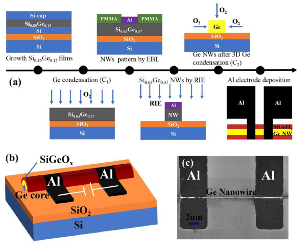
Figure 1. (a) Process flow, (b) schematic device diagram of Ge NW MSM photodetector on SiO2/Si substrates, (c) top view SEM image of Ge NW MSM photodetector.
Download figure:
Standard image High-resolution imageEBL was used to open contact holes in the selected areas of Ge NWs. After SiGeOx on the surface of Ge NWs was etched by buffered oxide etchant (BOE), 50 nm thick Al layer was sputtered and lifted off to form electrodes with 5 µm width and 9 µm space. The 3D schematic device diagram and scanning electron microscopy (SEM) top view image of Ge NW MSM photodetectors are shown in figures 1(b) and (c).
The surface morphology of the condensed Ge NW was characterized by SEM measurements. The chemical states of Ge oxides covering the surface of Ge layer were measured by XPS and Ge fraction in SiGe NWs were characterized by Raman spectra. Current–voltage (I–V) characteristics of Ge NW photodetectors were measured with Keithley 2611B. Photocurrent testing employs same test platform. First, the emitted light of halogen tungsten lamp was decomposed into monochromatic light using a monochromator, and then monochromatic light was introduced into the microscope through optical fiber to ensure that the spot was irradiated onto the photosensitive surface of NW photodetectors. The spectral response (I − λ) was calculated by measuring device current with a given bias with illumination at different wavelengths. The light source was used with a monochromator for illumination in the range of 400–2400 nm. The spectral test in this paper was to calibrate the spectral range of 360–1160 nm using standard Si (300–740 nm) and InGaAs (850–1750 nm) detectors.
3. Results and discussion
3.1. Structural characterization
The whole Ge condensation process as shown in figure 2(a), was carried out through two steps for preparation of pure Ge NW. In the first step, Si0.85Ge0.15 on SOI substrate was treated at 1150 °C for two cycles of 100 min oxidation and 30 min annealing. After that, Si1−xGex on insulator (SGOI) with Ge fraction x of 0.37 was obtained, as denoted C1. In this stage, SiO2 on the surface was removed by BOE, and stripe patterns with various widths were fabricated with EBL and RIE. These samples were then treated at 900 °C by several cycles of 10 min oxidation and 10 min annealing (referring as 3D Ge condensation) until pure Ge NW were achieved, as denoted C2. Raman spectroscopy has been employed to identify the crystalline quality and Ge component of Ge NW. Raman spectra of the as-grown, C1 and C2 samples during Ge condensation process are illustrated in figure 2(b). Raman spectra of bulk Ge is also given in this figure for comparison. The Raman signal was excited by a 532 nm laser with a spot size of 4 µm and a power of 20 mW. The following signals were detected including Si–Si peak (~520 cm−1) from Si, Si–Si (480–510 cm−1), Si–Ge (~400 cm−1) and Ge–Ge peaks (270–300 cm−1) from SiGe, respectively. The intensity ratio of Ge–Ge peak to Ge–Si peak increased with increase of Ge fraction. What important was that only Ge–Ge mode could be clearly observed in the sample at the final stage, indicating that almost pure Ge NW had been achieved. Compared with Ge–Ge line of bulk Ge, Ge NW should be under tensile strain of 1.2%, extracted from this difference between Ge–Ge peaks from bulk Ge and Ge NW. Ge is an indirect band gap material and the energy difference between direct conduction band (Г) and indirect conduction band (L) is about 136 meV at room temperature. When tensile strain is applied to Ge, the energy band gap is decreased and the energy difference between Г and L is also reduced, even changed to direct bandgap material. The light absorption is enhanced due to the direct band transition at longer wavelength.

Figure 2. (a) Oxidation process and annealing process of NWs prepared by Ge condensation method, (b) Raman spectra of a single NW with different Ge components, (c) top view of SEM image of a single Ge NW with 3D Ge condensation, (d) XPS spectra of oxide and Ge interface.
Download figure:
Standard image High-resolution imageThe typical SEM image of Ge NW prepared by Ge condensation technique is shown in figure 2(c). The width of Ge core is about170 nm and SiO2 shell is about 60 nm, respectively. The thickness of Ge is about 10 nm estimated with 3D condensation model, supposing the conservation of Ge during Ge condensation process, which has been definitely verified [24].
Chemical states of Ge oxides or SiGe oxides on Ge NW on insulator were characterized by XPS spectroscopy. Because what we concern was these chemical states of the Ge oxides near the Ge interface, the oxide layer on the Ge surface was thinned to 5 nm before measuring the XPS spectrum. The corresponding Ge 2p XPS spectra are depicted in figure 2(d), in which the broad Ge 2p electron binding energy peak has been decomposed into three valence states of Ge using a Lorentzian–Gaussian function. As can be seen, peaks around 1217.2 and 1220.6 eV [25] in Ge 2p XPS spectra is corresponding to Ge and GeO2, respectively. While the other Peaks around 1219.0 eV can be observed clearly, suggesting the existence of Ge suboxides. According to previous research, these following chemical reactions occur during Ge condensation process: Si + O → SiO2, Ge + O → GeO2, and Si + GeO2 → Ge + SiO2. Most part of the oxide is SiO2 [26]. Therefore, when excess oxygen is introduced into oxidation of almost pure Ge, a mixture of SiGeOx is formed near the Ge surface. Therefore, the XPS analysis confirm the formation of SiGeOx shell surrounding the Ge core with these existence of oxygen vacancies on the surface of NWs. The sub-stoichiometric oxides shell on the Ge core may provide oxygen vacancies, to be prone to charge trapping [16, 17, 19, 23].
3.2. Characterization of Ge NW photodetectors
In this part, these Ge NW MSM photodetectors with various widths of 35, 70 and 170 nm, were fabricated and characterized. Current–voltage characteristics of these three Ge NW photodetectors are presented in figure 3(a). Low dark current of 5.1 nA at 0.51 V bias for the 35 nm wide Ge NW photodetector indicates Ge NW with high crystal quality and good passivation. The Ge NW photodetector can be modeled as MSM devices with back-to-back Schottky diodes and thermionic emission (TE) as the dominant mechanism of carrier injection across the metal/semiconductor interface [27, 28]. It is found that this I–V curve can be fitted well by the thermionic emission theory as follows [29]:
where k, T, A* and  are Boltzmann's constant, absolute temperature, effective Richardson coefficient and barrier height, respectively. We thus find that schottky barriers (SBs) of Sample1 is 0.41 eV, Sample2 is 0.39 eV, and Sample3 is 0.40 eV for our MSM photodetectors in dark situation. The dark current increases sensitively with Ge NW width suggest that the bulk current, rather than surface leakage current, dominates the total dark current. This result implies that Ge NW surface is well passivated by SiGeOx formed during Ge condensation process in this case.
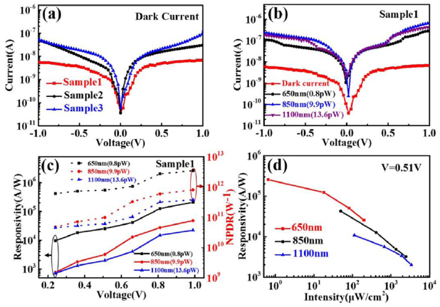
Figure 3. (a) I–V curves of Ge NW photodetectors under dark for Sample1, Sample2 and Sample3, (b) I–V curves of the Sample1 of Ge NW photodetector under dark and illumination of 650, 850 and 1100 nm light with power of 0.8, 9.9 and 13.6 pW, (c) dependence of responsivity and NPDR of the Ge NW photodetector on applied voltage at 650, 850 and 1100 nm, (d) dependence of responsivity of the Ge NW photodetector on optical power density at 650, 850 and 1100 nm.
Download figure:
Standard image High-resolution imageThe typical photocurrent of 35 nm wide Ge NW photodetector as a function of bias at fixed wavelengths of 650, 850 and 1100 nm is shown in figure 3(b). The large difference between photocurrent and dark current in one order of magnitude at very low illumination power indicates that the Ge NW photodetector has excellent performance. Otherwise, the almost same photocurrent from a commercial Si photodetector with a collection area of 1 mm2 and 35 nm wide, 9 µm long Ge NW photodetector at 1100 nm definitely demonstrates that responsivity of Ge NW photodetector is larger than that of a commercial Si photodetector by several order of magnitudes [30].
In figure 3(c), we plot the responsivity and normalized photocurrent to dark current ratio (NPDR) of the 35 nm wide Ge NW photodetector versus voltage at 650, 850, and 1100 nm wavelengths, respectively. The power incident on the NW has been estimated from the illumination intensity (measured in W cm−2) and the NW photosensitive surface area. The effective area of NW exposed for light absorption is approximately the sum area of top and sidewalls of Ge NW. According to structural parameters, these photosensitive surface areas are evaluated about 0.41, 0.72, and 1.62 µm2, respectively. The response spectrum of standard Si and InGaAs detector were used to calibrate the optical power corresponding to each wavelength of the light source. The NPDR is defined as [31]:
where Iphoto and Idark are photon and dark current, respectively; Pin is incident optical power; R is responsivity. It indicates that the responsivity and NPDR increases along with bias voltage linearly. Under 0.99 V bias, the responsivity is up to 2.09 × 10⁵ A W−1 at 650 nm and the NPDR value is about 3.48 × 10¹² W−1 at 650 nm. The NPDR is significantly higher than that of typical Si (~10 W−1), Ge (~102 W−1) and emerging 2D material (~102 W−1) photodetectors [32] suggesting promising application potential of Ge NW photodetectors.
Figure 3(d) depicts the dependence of responsivity on incident power at 650, 850 and 1100 nm, respectively, for the 35 nm wide Ge NW photodetector under 0.51 V bias. The responsivity decreases with increasing of incident power. A maximum responsivity of 2.55 × 10⁵ A W−1 was reached under illumination intensity of 0.65 µW cm−2 at 650 nm and 0.51V bias.
The response spectra of these three samples were measured in a wavelength range of 360 nm to 1160 nm, as shown in figure 4. Figure 4(a) displays response spectra of the 35 nm wide Ge NW photodetector under bias of 0.24, 0.36, and 0.51 V. The Ge NW photodetector shows strong response over the UV, visible and near-infrared wavelength (360–1160 nm). The large photo-responsivity up to 2.02 × 10⁵ A W−1 at 560 nm under 0.51 V is achieved, which is several orders of magnitude higher compared to those photodetectors made from bulk Ge (R ⩽ 1 A W−1) [33, 34]. The large responsivity can be attributed to large photocurrent gain of the Ge NW photodetector.

Figure 4. Response spectra of Ge NW photodetector under (a) various bias and (b) different sizes, (c) photocurrent gain versus wavelength for the photodetector with different NW sizes at 0.51 V bias, (d) spectral dependence of specific detectivity of the NW photodetectors with different NW sizes.
Download figure:
Standard image High-resolution imageFigure 4(b) displays the dependence of response spectra of Ge NW photodetectors on NW width under 0.51 V bias. It is indicated that responsivity increases with the reduction of Ge NW width in the whole studied wavelength range. Particularly, the responsivity of sample1 of 35 nm wide Ge NW photodetector is larger than that of sample3 of 170 nm wide Ge NW photodetector in beyond two orders of magnitude. This result can be attributed to large specific surface area for small size NW, in which traps at or near the interface between oxides and Ge play an important role in generation of photocurrent gain. The photocurrent gain of NW photodetector can be defined as [16]:
where Iphoto is photocurrent, Pin is the incident light power, R is responsivity, q is unit charge and hν is photon energy of incident light. Based on equation (3), the photocurrent gain is extracted for these samples under 0.51 V bias, as showed in figure 4(c). The gain increases with the decrease of Ge NW width and the peak value at 560 nm are 4.47 × 10⁶, 6.51 × 10⁵ and 6.31 × 10⁴ for these photodetectors of 35, 70 and 170 nm Ge NW width, respectively. The enormous gain is mainly due to these presence of oxygen vacancies at the interface between oxides and Ge, as reported previously [16–19]. These oxygen vacancies are prone to charge trapping to generate a radial electric field, which drives photo- electrons to the surface and be captured, resulting in an increase in the number of holes; In addition, a large number of holes accumulate at Al/Ge interface, causing the barrier to decrease and increasing the photocurrent.
The specific detectivity (D*) is another important parameter for characterization of photodetectors. The noise affecting D* consists of three parts: scattering noise from dark current, Johnson noise from thermal effect, and flicker noise. The main role is the scattering noise, so if we only consider the dark current. The specific detectivities of a photodetector are given by [35]:
Among them, R is responsivity, A is photosensitive surface, q is unit charge, and Idark is dark current. The unit of D* is cm·H1/2·W−1. Based on equation (4), the specific detectivity at 560 nm is extracted and shown in figure 4(d). The high detectivity of 1.26 × 10¹⁴, 2.54 × 10¹³ and 1.23 × 1013 cm·Hz1/2·W−1 for these samples of 35, 70, and 170 nm wide Ge NWs are obtained, respectively. Table 1 displays the summary of parameters of these samples.
Table 1. List of parameters of Ge NW photodetectors measured at 0.51 V bias.
| Nanowire name | Thickness (nm) | Width (nm) | Photosensitive surface A (um2) | electrode width (um) | Dark current (nA) | Responsivity (R) (A W−1) at 560 nm | Gain | D* (cm·Hz1/2·W−1) at 560 nm |
|---|---|---|---|---|---|---|---|---|
| Sample 1 | 10 | 35 | 0.41 | 5 | 5.1 | 2.02 × 10⁵ | 4.47 × 10⁶ | 1.26 × 10¹⁴ |
| Sample 2 | 10 | 70 | 0.72 | 5 | 16.2 | 2.94 × 10⁴ | 6.51 × 10⁵ | 2.54 × 10¹³ |
| Sample 3 | 10 | 170 | 1.62 | 5 | 21.5 | 2.85 × 10³ | 6.31 × 10⁴ | 1.23 × 10¹³ |
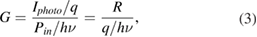
Based on above discussions, the large photocurrent gain of these Ge NW photodetectors could be well described in photogating effect [18, 36–38]. Figure 5 depicts the schematic diagram of photon carriers generation, trapping and effect on photocurrent gain in Ge NW photodetectors. The dark current of Ge NW photodetectors is assumed mainly governed by Schottky barrier height. The suboxide SiGeOx shell surrounding Ge cores provides a large number of oxygen vacancies at or near the surface of Ge NWs. The SiGeOx can induce a depletion layer on the Ge NW surface with a radial electric field from SiGeOx to inner NW. Oxygen vacancies serve as electron traps, rendering increase of lifetime of photon generated holes, which has great contribution to the gain. On the other hand, a large number of holes are gathered in the metal and semiconductor contact regions, lowering its Schottky barrier height, further enhancing photocurrent gain.
Figure 5. (a) Schematic diagram of photogeneration process of carriers in Ge NW, (b) schematic diagram of electron trapping process by the surface local states induced by SiGeOx on Ge NW, (c) schematic diagram of band alignment for the NW photodetector under thermal equilibrium and (d) under reverse bias.
Download figure:
Standard image High-resolution image
We summarize Ge NW photodetectors previewly reported and list their electrical parameters in table 2. The Ge NW photodetectors in this case show excellent properties in terms of low dark current and high specific detectivity.
Table 2. Performance comparison of the reported Ge NW photodetectors.
| Device (refs) | Dark current (nA) | Responsivity (R) (A W−1) | Gain | D* (cm·Hz1/2·W−1) |
|---|---|---|---|---|
| This work | 5.1 | 2.02 × 10⁵ | 4.47 × 10⁶ | 1.26 × 10¹⁴ |
| [19] | ~200 |
~1 × 10⁴ | ~2 × 10⁴ | 2.01 × 10¹² |
| [18] | ~600 |
~107 | ~107 | 5.65 × 10¹² |
| [16] | ~100 |
~2.80 × 10⁵ | ~2.10 × 10⁷ | 1.50 × 10¹³ |
| [17] | ~900 |
Not available | 103 | Not available |
aThis article has not given an accurate current value. This value is a rough value observed by the I–V curve. bThis article has not given an accurate D*. The rough value of D* is obtained by the calculation method in this paper.
4. Conclusion
High-specific-detectivity, low-dark-current Ge NW MSM photodetectors have been reported, in which Ge NWs were fabricated by 3D Ge condensation techniques. The excellent surface passivation by surrounded oxides formed during Ge condensation, as well as high crystal quality of Ge NWs and Schottky contacts, renders low dark current for Ge NW MSM photodetectors. Due to the surface defects states caused by SiGeOx on Ge NWs, Ge NW MSM photodetectors with high photocurrent gain have been achieved. A well-behaved Ge NW MSM photodetectors with a high responsivity of 2.02 × 10⁵ A W−1 at 560 nm and a low dark current of 5.1 nA under 0.51 V bias voltage is obtained. The high responsivity and low dark current of the Ge NW photodetector result in a high detectivity of 1.26 × 1014 cm·Hz1/2·W−1 at 560 nm under 0.51 V. Those results demonstrate that Ge NW MSM photodetectors are promising for applications in visible and near infrared wavelengths.
Acknowledgments
This work was supported by National Key Research and Development Program of China (2018YFB2200103); Natural Science Foundation of Jiangxi Province (20192ACBL20048).