

Abstract
In this paper, we demonstrate the design and characterization of a controllable dual-band terahertz metamaterial absorber formed by cascading a Salisbury-screen-like structure based on patterned graphene and a gold-graphene hybrid frequency selective surface. By electrostatically changing the chemical potentials of the graphene layers, absorptivity and operating frequency of the metamaterial absorber can be tuned independently without interference. Simulations indicate the absorptivity of the first absorbing peak can be varied from 35% to greater than 99% at 1.45 THz while the position of the second one can be tuned from 2.85 THz to 3.6 THz continuously with absorptivity of 90%. It provides a new perspective on the design of multiband tunable absorbers, thus promoting the realization of terahertz sensors and detectors for practical applications.
Export citation and abstract BibTeX RIS
Introduction
Terahertz metamaterial absorbers (TMAs) have attracted great attention because of their promising applications for detection and sensing, communication and stealth [1–5]. The operation frequency and absorptivity of TMAs, usually determined by materials and structures, keep unchanged once fabricated, which limits the scope of application. Therefore, the TMAs which can be dynamically tuned by means of external stimuli are highly desired. Traditional tuning techniques, such as diodes, varactors and liquid crystal, are generally restricted to lower frequencies since components are included in the construction [6]. The 2D material graphene is a promising candidate for designing tunable TMA due to unique properties including electrostatic control of conductivity, high electron mobility, high optical transparency and excellent mechanical properties [7–10].
Recently, numerous efforts have been focused on investigating tunable TMAs based on graphene. The frequency or absorptivity of TMAs can be controlled utilizing the patterned graphene, graphene-metal periodic hybrid, as well as the combination of monolayer graphene and metal patches [11–16]. To sustain high absorption, most of these research results indicate narrow bandwidth or limited numbers of operating bands. Various methods have been proposed to expand the bandwidth including multilayer structures, multiple resonators and gradual-width structure [17–22]. Besides, there is increasing interest in the dual graphene TMAs exploiting multilayer stack, dual-resonant structure and separated resonators [23–25]. However, most of these dual-band tunable graphene TMAs can only control a single variable (operating frequency or absorptivity) in the same manner. Moreover, the two bands are usually interrelated with each other so that some application requirements with high demand for independence of regulation cannot be satisfied. For example, frequency selective sensing desires to tune specific absorption band while keeping others fixed.
In this paper, an absorption-controllable graphene absorber and a frequency-tunable graphene absorber are cascaded together, thus constructing a dual-band tunable TMA. Firstly, the absorption-controllable band is emerged by a Salisbury-screen-like structure, which consists of a periodically patterned graphene layer placed over a dielectric layer backed on reflector. A perfect absorbing band is established when the input impedance of the absorber satisfies the impedance matching conditions with free space. Adjusting the chemical potential of the graphene changes the surface conductivity, then modulating the absorptivity, the modulation depth of which depends on the degree of impedance mismatch. Secondly, the frequency-tunable absorbing band is produced by a graphene-gold hybrid frequency selective surface (FSS), which plays the role of reflector in the absorption-controllable band while forms another adjustable absorber by itself. Graphene sheets, inserted into the key position of FSS, not only dissipate the energy of resonant point but also regulate the position of operating band due to the perturbation caused by the change of its chemical potential. It is numerically demonstrated through refined full-wave simulations that the two absorption bands with high isolation can be independently tuned.
Methods
Graphene can be modeled as an ultra-thin conducting surface whose surface conductivity consists of inter-band and intra-band transitions according to the Kubo formula [26, 27]:

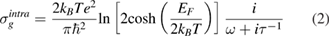

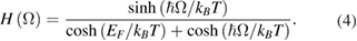
Where kB, e and  = h/2π are universal constant representing Boltzmann's constant, the charge of an electron and the reduced Planck's constant, respectively. EF is the chemical potential (Fermi energy), τ is the relaxation time set as 0.5 ps, T is room temperature set as 300 K and H(Ω) is defined as:
For low terahertz (THz) region, the inter-band contribution of graphene conductivity can be safely neglected considering Pauli exclusion principle [24]. The chemical potential EF can be tuned through the application of a bias voltage, thus modifying the conductivity of the graphene layer, then the resonance of TMA can be regulated effectively. In this paper, the numerical simulation is conducted in CST Microwave Studio. The absorption is calculated by A = 1 − R − T (or A = 1 − ǀS11ǀ2 − ǀS21ǀ2), where R and T represent the reflectance and the transmittance, respectively.
As shown in figure 1, the dual-band TMA with frequency/absorptivity-tunable properties is composed of two parts: a patterned graphene layer on the top and a graphene-gold hybrid FSS at bottom separated by the dielectric spacer. The blue arrow stands for the incident wave operating at first absorbing band f 1. Despite the waves absorbed by the patterned graphene, the rest is reflected or transmitted. Transmitted waves are reflected by the hybrid FSS and come back to the patterned layer with a phase difference π, so that the waves reflected by the graphene and FSS destructively interfere with each other, suppressing the total reflection and improving the absorbance. The red arrow represents the incident wave operating at second absorbing band f 2. Due to the graphene inserted in the resonant structure of FSS, the power is dissipated within the FSS. The black arrow symbolizes the waves outside the operating frequency band. Some of them are reflected by the patterned layer while others are reflected by the hybrid FSS with little attenuation. The size of arrows represents the energy it contained. The FSS with two layers tunes the absorbing frequency f 2 via changing the interlayer voltage, which affects the properties of graphene inserted into the resonant structure of FSS. The patterned graphene layer should be nearly transparent at the frequency-tunable absorbing band f 2 while functions as a Salisbury-screen-like structure along with the FSS at the other absorbing band f 1, which locates at the rejection band of the FSS. The absorptivity of Salisbury-screen-like structure depends on the impedance matched and mismatched condition, affected by the surface conductivity directly.

Figure 1. Profile sketch of the dual-band TMA.
Download figure:
Standard image High-resolution imageFirstly, an absorption-controllable terahertz metamaterial absorber is designed. The patterned graphene monolayer, such as disks, ribbons and square rings, can be modeled as the series circuit of Rg, Lg and Cg [28–30]. Then, the dielectric, whose length tp 1 approaches λp /4 wavelength of f 1, is equivalent to a transmission line with characteristic admittance Yp . The reflector is viewed as short terminal, which will transform into an open end after the quarter wavelength conversion section. Therefore, the input admittance Yin can match with the admittance of free space Y0 via designing the pattern and tuning the chemical potential of graphene to adjust the value of Rg, Lg and Cg. Hence, the perfect absorption is obtained when Rg = 1/Y0 and  . The variation of chemical potential leads to the mismatch of admittance, shaping an absorption-controllable band.
The structure of the absorption-controllable TMA is shown in figure 2, which consists of a patterned graphene layer, a SiO2 layer, a p-type doped Si layer, a polyimide layer and a gold ground. The connected graphene disks not only ensure the polarization independent due to C4 symmetric but also solve the feed problem of separated units. p denotes the period of the unit cell; r represents the radius of the disk; w indicates the width of the connector. The thin doped Si layer (εsi = 11.9 [31]) with thickness tsi acts as the other gate electrode to apply a DC bias; the SiO2 ( = 4 [13]) with thickness
  plays the role of partitions; The polyimide (εp = 3.5 + 0.02i [32]) with thickness tp 1 is used as quarter-wavelength impedance transformer; the gold ground with conductivity of 4.561 × 10⁷ S m−1 serves as reflector. It should be noted that the gold ground will be replaced by a hybrid FSS in the design of the dual-band TMA so that the doped Si layer, instead of the gold bottom, is used to tune the chemical potential of patterned graphene, thus realizing independent regulation. The thicknesses of Si and SiO2 are extremely thin compared with the operating wavelength. Therefore, the dielectric layers still function as a transformer to sustain impedance matching. The thickness of polyimide optimized by CST is a little thinner than the value of theoretical calculation because of the introduction of Si and SiO2 layers. Besides, the thickness of ground tAu should be much larger than typical skin depth in THz.

Figure 2. Structure of the absorption-controllable TMA. The values of the structure parameters are set as p = 55, r = 16.5, w = 6.6,  = 1, tsi = 1, tp 1 = 26.7, tAu = 0.5, unit: μm.
Download figure:
Standard image High-resolution imageSecondly, a graphene-gold hybrid frequency selective surface is designed to construct a frequency-tunable absorbing band. The hybrid FSS is composed of two periodic layers separated by a thin dielectric substrate. The front layer is consisted of a loop slot array inserted with graphene patches. The loop slot array can be modeled as the parallel of Lf and Cf while the graphene patches are viewed as the series model of  and
and  paralleled with Cf [33–37]. The back layer is consisted of strips serving as a gate electrode. The FSS constitutes a bandpass resonance, but the energy at the resonance point is dissipated by
  , thus forming an absorbing peak. Regulating the voltage between the layers, the chemical potential of graphene changes gradually, so does
  and
and  , thus the position and bandwidth of the absorbing point can be controlled.
As illustrated in figure 3, the simulated structure of the hybrid FSS has double gold layers divided by a thin polyimide layer with thickness tp 2. The front gold layer is a ring aperture array, whose period, inner and outer diameters are denoted as l, rin and rout, respectively. Graphene strips with width d are evenly deposited at the bottom of the ring aperture. The back layer is a gold grid with width g, which acts as a gate electrode to provide bias voltage. By changing the bias voltages between layers, the resonant point of the FSS is controlled over a relatively broad range of frequency band.

Figure 3. Structure of the hybrid FSS. The values of the structure parameters are set as l = 27.5, rout = 12.38, rin = 11.14, d = 10, g = 9, tp 2 = 10, tAu = 0.5, unit: μm.
Download figure:
Standard image High-resolution imageFinally, substituting the hybrid FSS for the gold ground of the Salisbury-screen-like structure, a dual-band tunable TMA is constructed. The periodicity of the patterned graphene layer was twice as large as that of the FSS, so one unit of the top layer and four units of FSS are combined together in the simulation.
Results and discussion
Assuming a THz plane wave impinges on the absorption-controllable TMA, the absorption can be controlled via bias voltage between the patterned graphene layer and doped Si layer. The approximate theoretical relation between EF and Vg is [38, 39]

where vF = 106 m s−1 is the Fermi velocity, ε0 is the permittivity of the vacuum, εr is the permittivity of the substrate between graphene and electrode, Vg is the bias voltage, e is the electron charge, and ds is the thickness of the silicon dioxide layer. As shown in figure 4, the EF1 is tuned from 0.1 eV to 0.5 eV that when external voltages are changed from 40 V to 810 V. However, the voltage can be greatly decreased by reducing the thickness of SiO2 without affecting the overall performance except slight frequency shift. Besides, chemical doping for the graphene can also help decrease the required voltage since the chemical potential does not start from 0 in our research.

Figure 4. The approximate relation between the gate voltages and the chemical potential.
Download figure:
Standard image High-resolution imageThe absorptions for different chemical potentials are calculated and displayed in figure 5. The 90% absorption band ranges from 1.34 THz to 1.62 THz with a perfect absorbing peak f 1 at 1.45 THz when EF1 = 0.5 eV. Further, varying the chemical potential of graphene by applying static electric field in the patterned graphene layer and doped Si layer, the absorption spectrum is shown in figure 5(b). As EF1 decreases from 0.5 eV to 0.1 eV, the maximum absorptivity drops to 0.35 and the f 1 exhibits slight red shift. For patterned graphene layer, Rg and Lg are the inverse proportional functions of the chemical potential while Cg is not affected by it in low THz region [33, 34]. The reflectance R is determined by
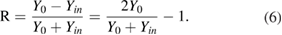

Figure 5. Absorption spectra of the absorption-controllable TMA (a) EF1 = 0.5 eV, 0.1 eV (b) as a function of frequency and EF1.
Download figure:
Standard image High-resolution imageAt the position of the absorbing peak f 1, Yin is primarily determined by 1/Rg. Rg significantly grows with the decreases of EF1, so then R increases remarkably, leading to the decline of absorptivity [30]. At the same time, Lg grows gradually, resulting in the slight fall of resonance frequency due to  . Although the thickness of polyimide layer tp 1 is no longer strictly equal to the quarter wavelength of f 1 due to the slight frequency shift, it has limited effect on the performance compared with the increment of Lg. Through biasing at different voltages to turn EF1, the absorption of TMA can vary between 35% and 99.99% at low THz region.
Then the spectrum response of the FSS with chemical potential EF2 = 0.5 eV is indicated in figure 6(a). There is a resonant point at 4.4 THz, whose absorbance, reflectance and transmittance are 0.8, 0.02 and 0.18, respectively. As shown in figure 1, the FSS is placed under a polyimide layer with thickness tp 1 when constructing the dual-band TMA. Adding dielectric slab with finite length to the one side of FSS will shift the original resonant frequency f 0 to the position between f 0 and  , where εr represents the relative permittivity of the dielectric slab [40]. The resonant frequency f 2 of the FSS drops to 3.6 THz after integrating with the polyimide layer. Besides, the absorption rises to 0.9 due largely to the loss of the additional polyimide slab. Further, the absorption spectrum under different chemical potential is depicted in figure 6(b). As EF2 varies from 0.5 eV to 0.1 eV, the absorption peak red-shifts from 3.6 THz to 2.85 THz. Meanwhile, the effective absorbing bandwidth is slightly narrowed. There is a negative correlation between the chemical potential and values of
  and
and  [31, 32]. Besides, the resonance frequency is inversely associated with total paralleled inductance, which increases with the growth of Lg. Therefore, the resonant point moves towards to lower frequency with the drop of chemical potential. The narrower bandwidth results from the increase of
  , which has a direct impact on quality factor of resonance.

Figure 6. (a) Reflectance, transmittance and absorption through the hybrid FSS with/without polyimide layer. (b) Absorption spectra of the hybrid FSS as a function of frequency and EF2.
Download figure:
Standard image High-resolution imageThe slot arrays, such as square ring, circular ring, cross-loop slot, can take shape a LC parallel resonance and construct a transmission peak [40]. Most of the resonant energy triggered by the incident wave focuses on the slot along the direction of incident electric field. Therefore, depositing lossy materials in the electric field gathering place will effectively dissipate the power of the incident wave and transform the transmission band into an absorption band. Figure 7(a) gives the distribution of electric field on the top surface of the FSS at 3.6 THz when EF2 = 0.5 eV, thus giving a better understanding for absorption peak. There is a strong electric field concentrating on the narrow gap along the direction of incident electric field, which will be dissipated by the graphene. Moreover, C4 symmetric of the graphene slices distributing in the ring contributes to polarization independent of the absorber. Except the absorption of graphene, the gold resonant units also make contributions to the loss of energy in Terahertz, thus forming a resonant peak with high absorption. To give a straightforward analysis to the loss, the energy distributions of incident wave are show in figure 7(b). It can be seen that most of energy at the resonant frequency is absorbed by the graphene. Further, the polyimide and gold also enhance the absorption.

Figure 7. (a) The distribution of electric field on the top surface of the FSS at 3.6 THz when EF2 = 0.5 eV. (b) The energy partition of incident wave at 3.6 THz when EF2 = 0.5 eV.
Download figure:
Standard image High-resolution imageTo further analyze the function of the FSS, figure 8 gives the sectional view of the simulated electric field intensity distributions at 1.45 THz and 3.6 THz along with incident direction when EF2 = 0.5 eV. In figures 8(a) and (b), f 1 = 1.45 THz, the position of wave peak remains unchanged while the intensity of electric field shows a sharp decline when the phase of the incident wave increases from 0° to 90°. In other words, a typical standing wave is formed, which means that nearly all energy is reflected. Therefore, the FSS can act as the gold ground of the absorption-controllable TMA. In figures 8(c) and (d), f 2 = 3.6 THz, the wave peak of the electric field moves towards the surface of the FSS while the variation of electric field intensity is not obvious with 90° phase shift. There is a traveling wave above the absorber due to the little reflection. Moreover, most of the incident electric field centers on the ends of the ring aperture, verifying the incident power is mainly dissipated on the graphene inserted in the top layer. The FSS not only plays the role of a reflector at f 1 but also functions as an absorber at f 2.

Figure 8. Cross section of the electric field intensity when EF2 = 0.5 eV. (a) 1.45 THz, phase = 0° (b) 1.45 THz, phase = 90° (c) 3.6 THz, phase = 0° (d) 3.6 THz, phase = 90°.
Download figure:
Standard image High-resolution imageReplacing the gold ground of the Salisbury-screen-like structure with the hybrid FSS, a dual-band tunable TMA is constructed. The absorption-controllable band f 1 is attributed to the impedance matching of Salisbury-screen-like structure while the frequency-tunable absorbing band f 2 is caused by the dissipation of the hybrid FSS. Both two absorbing bands can be controlled individually without one impacting the other. Figure 9(a) shows the absorption of the dual-band tunable TMA as function of the frequency of operation and chemical potential of the patterned graphene. When EF1 varies from 0.5 eV to 0.1 eV with EF2 = 0.5 eV, the absorbing peak locating at f 1 = 1.45 THz falls from perfect absorption to 0.35. However, the absorptivity of the second peak at f 2 = 3.6 THz remains over 90% for the fixed EF2. Figure 9(b) illustrates the relation between the absorption spectrum and EF2 with EF1 fixed at 0.5 eV. The absorbing characteristics at f 1 are almost invariable while f 2 moves from 3.6 THz to 2.85 THz with absorptivity of 0.9. Briefly, the spectrum of the dual-band tunable TMA is the superposition results of absorption-controllable TMA and frequency-tunable absorbing FSS. Due to the design of the separated bias structure, the absorption of f 1 and the position of f 2 can be tuned independently and flexibly.

Figure 9. Absorption spectra of the dual-band TMA as a function of frequency and chemical potential (a) EF1 = 0.5 eV, 0.1 eV, EF2 = 0.5 eV (b) EF1: 0.1–0.5 eV, EF2 = 0.5 eV (c) EF1 = 0.5 eV, EF2 = 0.5 eV, 0.1 eV (d) EF1 = 0.5 eV, EF2: 0.1–0.5 eV.
Download figure:
Standard image High-resolution image
It should be emphasized that the design concept of tunable dual-band TMA with high isolation provides new degrees of freedom and flexibility. The relative position of absorption-controllable band and frequency-tunable band can be reversed via adjusting the resonant frequency of circuit model. In theory, the idea of cascading a hybrid FSS is available to add extra tunable absorbing band for absorbers with fully reflecting bottom, if two condition are satisfied: (i) the absorber does not reflect or absorb the incident wave operating at f 2 after removing the reflecting bottom; (ii) the hybrid FSS completely reflects the incident wave operating at f 1. For example, replacing the Salisbury-screen-like structure with the Jaumann-screen-like structure can build a TMA with a switchable broad absorbing band and a frequency-tunable narrow absorbing band.
Moreover, the transmission/absorption characteristic of f 2 can be adjusted according to actual demand. Except the absorbed waves, the others are reflected and transmitted by the FSS at f 2. Adding a dielectric layer backed on metallic film to the bottom of the FSS can construct a cavity. Transmitted waves are reflected by the metallic film and destructively interfere with reflected waves, enhancing the absorption of f 2 further. In addition, the frequency-tunable absorbing band will be replaced by a fixed passband once the graphene inserted into the FSS is removed. These methods greatly expand the application range and prospect of TMAs.
Conclusions
A dual-band terahertz metamaterial absorber based on graphene has been designed and demonstrated theoretically. The absorptivity and operating frequency of the two absorbing peaks can be tuned separately by electrostatically controlling chemical potentials of different graphene layers. Changing the voltage between the patterned graphene and doped Si, the absorption at 1.45 THz can switch to reflection because of the impedance mismatch with free space. Varying the voltage between two layers of the FSS, the absorbing peak with 90% absorptivity moves from 2.85 THz to 3.6 THz since the resonant frequency of the FSS is also changed. The idea of replacing ground of absorbers with a FSS offers a promoting method to increase extra absorption or transmission band for tunable absorbers. Besides, the design concept is available to other terahertz region for various promising applications due to the scalability of periodic structure.
Acknowledgments
This work was supported by National Natural Science Foundation of China (NSFC) (61801485).