

Abstract
Four Al0.52In0.48P p+-i-n+ mesa photodiodes with 6 μm thick i layers and two different diameters (217 μm ± 15 μm and 409 μm ± 28 μm) were studied at room temperature (24 °C). Electrical characterisation measurements are reported along with measurements showing the performance of the devices as x-ray detectors. The devices exhibited leakage currents <3 pA (corresponding to leakage current densities <2 nA cm−2) at 100 V reverse bias (electric field strength of 167 kV cm−1). The photodiodes were coupled to a custom-made low-noise charge-sensitive preamplifier, the noise characteristics of the resultant spectrometers were investigated as functions of shaping times. The best energy resolutions (full width at half maximum of the 5.9 keV photopeak from an 55Fe radioisotope x-ray source) achieved with the 217 μm ± 15 μm and 409 μm ± 28 μm diameter photodiodes were 0.89 keV and 1.05 keV, respectively. The dielectric dissipation factor of Al0.52In0.48P was estimated to be (2.2 ± 1.1) × 10−3 at room temperature.
Export citation and abstract BibTeX RIS
1. Introduction
The wide bandgap (Eg = 2.31 eV at room temperature [1]) compound semiconductor Al0.52In0.48P has started to emerge as a promising material for use in high temperature (>20 °C) x-ray detectors [2–4]. A number of other wide bandgap semiconductor materials have also received research attention for the same application, including: 4H-SiC [5, 6] (Eg = 3.27 eV at room temperature [7]); GaAs [8] (Eg = 1.42 eV at room temperature [9]); Al0.8Ga0.2As [10] (Eg = 2.09 eV at room temperature [11]); and In0.5Ga0.5P [12] (Eg = ~1.9 eV at room temperature [13]). X-ray photodiodes made from such wide bandgap materials can have lower leakage currents than comparable detectors made from traditional narrower bandgap materials such as Si (Eg = 1.12 eV at room temperature [14]) and Ge (Eg = 0.67 eV at room temperature [15]). It is common for Si and Ge detectors to require cooling (sometimes to low temperatures, e.g. −120 °C [16]) to obtain sufficiently low leakage currents for optimum operation; this is because the parallel white noise of an x-ray spectrometer is proportional to the detector's leakage current [17]. Cooling systems increase the mass, volume, power consumption, and cost of x-ray spectrometers, thus preventing their use in some environments and situations. As such, considerable effort has been made to develop systems that can operate without cooling, particularly for space science and astronomy, where instrument mass, volume, and power consumption are severely restricted [18]. In addition, there are numerous other applications where uncooled operation at high temperatures is beneficial, including nuclear decommissioning and the detection and interdiction of contraband nuclear materials.
One benefit of Al0.52In0.48P over many other wide bandgap materials so far demonstrated for photon counting x-ray detection is its high x-ray linear absorption coefficients, μ. For example, at 5.9 keV, Al0.52In0.48P has a substantially higher linear absorption coefficient (μ5.9 keV = 1302 cm−1) than 4H-SiC (μ5.9 keV = 346 cm−1), Al0.8Ga0.2As (μ5.9 keV = 640 cm−1), and GaAs (μ5.9 keV = 837 cm−1) [19]. This leads to a higher quantum detection efficiency for a given detector thickness. The first reported Al0.52In0.48P x-ray detectors were avalanche photodiodes with an avalanche region of 1 μm [2]. Subsequently, thicker (2 μm i layer) non-avalanche Al0.52In0.48P p-i-n photodiodes were also demonstrated [3, 4]. As well as improving the detector's quantum efficiency, thicker i layers can also improve spectrometer energy resolutions by virtue of the thicker i layer resulting in a lower detector capacitance. Lower capacitance results in reduced capacitance-dependent electronic noise (e.g. series white noise (including the induced gate current noise), 1/f series noise, and dielectric noise).
In this paper, results are presented of the characterisation of four Al0.52In0.48P p+-i-n+ mesa x-ray photodiodes with 6 μm thick i layers. Photodiodes with two different areas (217 μm ± 15 μm diameter, D1 and D2; 409 μm ± 28 μm diameter, D3 and D4) were electrically characterised at room temperature (24 °C). The photodiodes were then studied as photon counting spectroscopic detectors using an 55Fe radioisotope x-ray source (Mn Kα = 5.9 keV; Mn Kβ = 6.5 keV). The Al0.52In0.48P structures are the thickest so far reported (by a factor of 3) that have been grown with metalorganic vapour phase epitaxy (MOVPE) for this application.
2. Materials and device structure
Al0.52In0.48P p+-i-n+ epilayers were grown lattice matched on a commercial (1 0 0) GaAs n+ substrates by metalorganic vapour phase epitaxy (MOVPE) at the EPSRC National Epitaxy Facility, Sheffield, UK. The details of the epilayer are summarised in table 1. Chemical etching techniques were used to fabricate circular mesa photodiodes of two different sizes (≈200 μm and ≈400 μm). Initially, the etching was started using a 1:1:1 H3PO4:H2O2:H2O solution. However, because of the slow vertical etch rate achieved, the etching recipe was modified. Thereafter, a 1:1:1 K2Cr2O7:HBr:CH3COOH solution followed by 10 s in a 1:8:80 H2SO4:H2O2:H2O solution was used. The diameters of the devices were measured after fabrication to be 217 μm ± 15 μm (D1 and D2) and 409 μm ± 28 μm (D3 and D4), respectively. The stated uncertainties reflect the accuracy of the optical microscope calibration rather than variation of diameter between devices intended to be of the same size.
Table 1. Layer details of the Al0.52In0.48P wafer.
| Layer | Material | Thickness (μm) | Dopant | Dopant type | Doping density (cm−3) |
|---|---|---|---|---|---|
| 1 | GaAs | 0.01 | Zn | p+ | 1 × 10¹⁹ |
| 2 | Al0.52In0.48P | 0.2 | Zn | p+ | 5 × 10¹⁷ |
| 3 | Al0.52In0.48P | 6 | Undoped | ||
| 4 | Al0.52In0.48P | 0.1 | Si | n+ | 2 × 10¹⁸ |
| 5 | Substrate n+ GaAs |
Top Ohmic annular contacts, Ti/Au (20 nm/200 nm), was evaporated on the GaAs p+ layer of each device. The areas covered by the top contacts were 0.014 mm2 and 0.041 mm2 on the 217 μm and 409 μm diameter photodiodes, respectively. An optical microscope photograph showing the geometry of the top contacts is presented in figure 1. A planar rear Ohmic contact, InGe/Au (20 nm/200 nm), common to all devices on the die, was evaporated onto the reverse of the GaAs n+ substrate. The detectors were all packaged in a TO-5 can.

Figure 1. Photograph of the photodiodes showing the geometry of the top contacts. The photodiodes at the bottom of the figure are the 409 μm diameter devices; the photodiodes at the top are the 217 μm diameter devices.
Download figure:
Standard image High-resolution imageSince the surfaces of the photodiodes were partially covered by the Ohmic annular contacts, the weighted quantum efficiency (considering the areas covered and uncovered by the contacts) for the devices were calculated using the Beer–Lambert law, and assuming 100% charge collection in the epitaxial p and i layers. The weighted quantum efficiencies as functions of incident x-ray energy (up to 10 keV) for the 217 μm diameter photodiodes (D1 and D2) and 409 μm diameter photodiodes (D3 and D4) are presented in figure 2. The weighted quantum efficiencies of the photodiodes were calculated to be 0.529 at 5.9 keV and 0.450 at 6.49 keV for D1 and D2, and 0.535 at 5.9 keV and 0.454 at 6.49 keV for D3 and D4.

Figure 2. Calculated weighted quantum efficiencies of the Al0.52In0.48P p+-i-n+ mesa photodiodes as functions of x-ray photon energy: 409 μm diameter photodiodes (D3 and D4, solid line); 217 μm diameter photodiodes (D1 and D2, dashed line). The discontinuities are the Al K, P K, and In L x-ray absorption edges.
Download figure:
Standard image High-resolution image3. Experimental method, results and discussions
3.1. Electrical characterisation
3.1.1. Capacitance-voltage measurements.
The capacitances of the two 217 μm ± 15 μm diameter (D1 and D2) and the two 409 μm ± 28 μm diameter (D3 and D4) packaged Al0.52In0.48P photodiodes were measured in a dry N2 environment (relative humidity <5%) at room temperature (24 °C) using an HP 4275A Multi Frequency LCR meter and a Keithley 6487 Picoammeter/Voltage Source as the external voltage supply. The LCR meter was set with a 60 mV r.m.s AC test voltage signal magnitude and a 1 MHz frequency. National Instruments Labview software was used to automate the capacitance measurements. Each photodiode was reverse biased up to 100 V, with increments of 1 V. The capacitance of the device's package was estimated by measuring the capacitances between the empty pins on the package (pins without photodiodes connected to them) and the common pin of the package, it was found to be 0.84 pF ± 0.05 pF. In order to find the capacitance of the device itself, the capacitance of the device's package was subtracted from the measured capacitance of the packaged device.
The depletion width (W) of each photodiode was considered to be given by,
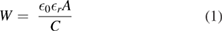
where  0 is the permittivity of the vacuum, r is the relative permittivity of Al0.52In0.48P (11.25 [20]), A is the area of the photodiode, and C is the capacitance of the photodiode.
The capacitances and the associated depletion widths of the photodiodes as functions of applied reverse bias are shown in figures 3 and 4, respectively. The capacitance densities of these photodiodes were found to be similar across the investigated biases and become relative constant (5 pF mm−2 ± 1 pF mm−2) at high reverse biases (>80 V). At 100 V reverse bias, the capacitances of the 217 μm diameter photodiodes (D1 and D2) were found to be 0.71 pF ± 0.07 pF and 0.66 pF ± 0.07 pF, respectively; and the capacitances of the 409 μm diameter photodiodes (D3 and D4) were found to be 2.48 pF ± 0.09 pF and 2.49 pF ± 0.09 pF, respectively.

Figure 3. Measured capacitances of the Al0.52In0.48P p+-i-n+ mesa photodiodes, 217 μm diameter photodiode (D1, + symbols; D2, × symbols); 409 μm diameter photodiode (D3, open circles; D4, open squares), as functions of applied reverse bias at room temperature (24 °C).
Download figure:
Standard image High-resolution image
Figure 4. Calculated depletion width of the Al0.52In0.48P p+-i-n+ mesa photodiodes as functions of applied reverse bias at room temperature (24 °C). 217 μm diameter photodiode D2 (×symbols); 409 μm diameter photodiode D4 (open squares). For clarity, only data for one diode of each size are shown, but comparable results were obtained for the other devices.
Download figure:
Standard image High-resolution imageAt the highest investigated reverse bias (100 V), the calculated depletion widths and associated uncertainties (including the error in the diameter of these photodiodes, the uncertainties in the capacitance measurements, and the Debye length) of the photodiodes were found to be 5.13 μm ± 0.87 μm and 5.57 μm ± 0.98 μm for the 217 μm diameter photodiodes (D1 and D2), and 5.26 μm ± 0.75 μm and 5.26 μm ± 0.75 μm for the 409 μm diameter photodiodes (D3 and D4). Reduction of capacitance with increasing reverse bias became insignificant at reverse biases >80 V. These devices have a thicker depletion region than the previously reported Al0.52In0.48P x-ray detectors (i layer thickness of 0.5 μm with an avalanche layer thickness of 1 μm [2]; i layer thickness of 2 μm [3]).
3.1.2. Current–voltage measurements.
Leakage currents as functions of applied reverse bias for the four Al0.52In0.48P photodiodes were measured in dark condition in a dry N2 environment (relative humidity <5%) at room temperature (24 °C). Using a Keithley 6487 Picoammeter/Voltage Source, each photodiode was reverse biased from 0 V to 100 V, in increments of 1 V. National Instruments Labview software was used to automate the measurements. Low leakage currents (<3.0 pA ± 0.4 pA) (including the package's leakage current) were found for all the photodiodes even at high reverse bias (100 V), as shown in figure 5. The leakage current associated with the package itself was estimated by measuring the leakage current of an empty pin on the same package and common pin of the package. The package's leakage current was found to be less than the picoammeter's uncertainty (0.4 pA). Hence, the package's leakage current was considered to be negligible.

Figure 5. Leakage currents as functions of applied reverse bias for the Al0.52In0.48P p+-i-n+ mesa photodiodes, 217 μm diameter photodiode (D1, + symbols; D2, × symbols); 409 μm diameter photodiode (D3, open circles; D4, open squares), at room temperature (24 °C).
Download figure:
Standard image High-resolution imageAt 40 V reverse bias (electric field strength ≈ 105 kV cm−1), the leakage current densities of the Al0.52In0.48P photodiodes (217 μm diameter devices, D1 = 0.34 nA cm−2, D2 = 0.24 nA cm−2; 409 μm diameter devices, D3 = 0.03 nA cm−2, D4 = 0.08 nA cm−2) were greater than has been reported with custom-made SiC x-ray detectors (e.g. 1 pA cm−2 at an electric field strength of 103 kV cm−1 at room temperature [21]) but comparable to the leakage current densities reported with commercially available SiC UV detectors (1.2 nA cm−2 at electric field strength of 227 kV cm−1 at room temperature [6]). In contrast, the leakage current densities of the Al0.52In0.48P photodiodes were lower than has been reported for semi-insulating SiC x-ray photodiodes (65 nA cm−2 with internal electric field of 28 kV cm−1 at room temperature [22]) and Al0.8Ga0.2As photodiodes (4.72 nA cm−2 with an electric field of 29 kV cm−1 at room temperature [10]).
3.2. Photon counting x-ray spectroscopy
The four packaged photodiodes were each in turn soldered to a wire-ended packaged silicon input JFET (2N4416A, capacitance = 2 pF) which was the first transistor of a custom-made low-noise charge-sensitive preamplifier of feedback resistorless design [23]. An ORTEC 572A shaping amplifier and an ORTEC EASY-MCA 8k multi-channel analyser (MCA) were connected to the preamplifier. The photodiodes were each in turn illuminated with an 55Fe radioisotope x-ray source (Mn Kα = 5.9 keV; Mn Kβ = 6.5 keV; activity = 175 MBq). The 55Fe radioisotope x-ray source was placed 4 mm above the 217 μm diameter photodiodes and 10 mm above the 409 μm diameter photodiodes. In each case, the system was investigated at six different shaping times (0.5 μs, 1 μs, 2 μs, 3 μs, 6 μs, and 10 μs) with each photodiode reverse biased at 0 V, 10 V, 20 V, 30 V, 40 V, 60 V, 80 V, and 100 V. Each spectrum was accumulated for 240 s. The photodiodes and the preamplifier were operated at room temperature (24 °C) in a dry N2 environment (relative humidity <5%).
The resulting spectra were calibrated in energy terms by using the positions of the zero energy noise peak and the fitted Mn Kα peak at 5.9 keV for each spectrum as points of known energies on MCA's charge scale, and assuming a linear variation of detected charge with energy. The energy resolutions (FWHM at 5.9 keV) of the systems as functions of shaping times are shown for a detector reverse bias of 100 V in figure 6. The best energy resolutions of the 217 μm diameter photodiode (D2) and 409 μm diameter photodiodes (D4) at each reverse bias are presented in figure 7. FWHM at 5.9 keV as good as 0.89 keV ± 0.04 keV and 1.05 keV ± 0.08 keV were found for the 217 μm diameter photodiode (D2) and the 409 μm diameter photodiode (D4), respectively, at 100 V reverse bias. Figure 8 shows the spectra obtained with each photodiode at the best shaping time when reverse biased 10 V, 20 V, 40 V, and 100 V.

Figure 6. Measured FWHM at 5.9 keV as a function of shaping time when the photodiodes were operated at an applied reverse bias of 100 V: 217 μm diameter photodiodes D1 (+symbols) and D2 (×symbols); 409 μm diameter photodiodes D3 (open circles) and D4 (open squares).
Download figure:
Standard image High-resolution image
Figure 7. Measured FWHM at 5.9 keV of one of the 217 μm diameter photodiodes (D2, × symbols), and one of the 409 μm diameter photodiodes (D4, open circles), as functions of applied reverse bias at the optimum shaping time.
Download figure:
Standard image High-resolution image
Figure 8. 55Fe x-ray spectra obtained with (a) one of 217 μm diameter photodiodes (D2), (b) one of 409 μm diameter photodiodes (D4), at varying reverse biases (for clarity only 10 V, dash line; 20 V, dot line; 40 V, dash dot line; 100 V, solid line, are shown). The shaping time which gave the best energy resolution was selected at each reverse bias. The FWHM at 5.9 keV of D2 were 0.89 keV, 0.91 keV, 0.93 keV, and 0.97 keV at the reverse bias of 100 V, 40 V, 20 V, and 10 V, respectively. The FWHM at 5.9 keV of D4 were 1.05 keV, 1.11 keV, 1.19 keV, and 1.36 keV at the reverse bias of 100 V, 40 V, 20 V, and 10 V, respectively.
Download figure:
Standard image High-resolution imageThe energy resolutions obtained (0.89 keV and 1.05 keV at 5.9 keV, for the 217 μm and 409 μm diameter detectors, respectively) are not as good as some of those obtained using other wide bandgap x-ray photodiodes at room temperature. For example, a 200 μm diameter GaAs mesa photodiode spectrometer had a FWHM at 5.9 keV of 745 eV [24], and a 200 μm × 200 μm SiC x-ray pixel detector had a FHWM at 5.9 keV of 196 eV at 30 °C when coupled to lower noise readout electronics [21]. However, the energy resolutions achieved with these AlInP devices are better than those previously reported for 2 μm i layer AlInP mesa devices (0.93 keV for a 200 μm diameter photodiode; 1.2 keV for a 400 μm diameter photodiode [3]). They are also better than has been reported with some other custom wide bandgap photodiodes, e.g. AlGaAs (1.07 keV at 20 °C for a 200 μm diameter diode [25], 1.06 keV at 20 °C for a 200 μm diameter photodiode [26]). A shaping time noise analysis is presented in section 3.3.
The valley-to-peak (V/P) ratio (as defined as the ratio between the number of counts at 4.1 keV and 5.9 keV) at the optimum shaping time and the greatest investigated reverse bias (100 V) were 0.048 and 0.058 for the 217 μm diameter photodiode (D2) and the 409 μm diameter photodiode (D4), respectively. These are not as good as those reported for cooled silicon DEPFET detectors (V/P = ~0.0001) [27] and GaAs detectors (V/P = 0.03) [28], but better than those of some AlGaAs photodiodes (V/P = 0.08 [10, 26]). The low energy tail of the photopeak which gives rise to the valley is a consequence of the partial collection of charge created by x-ray photons absorbed in the semiconductor layers often assumed to be inactive (e.g. substrate) [10]. The V/P ratio is therefore expected to improve as AlInP detectors with thicker i layers are grown.
Figure 9 shows how the number of counts in the 5.9 keV photopeak changed as the reverse bias was increased. The number of counts was found to increase from 5.79 × 10⁶ at 0 V reverse bias to 5.94 × 10⁷ at 100 V reverse bias for the 217 μm diameter photodiode (D2), and from 3.40 × 10⁶ at 0 V reverse bias to 4.39 × 10⁷ at 100 V reverse bias for the 409 μm diameter photodiode (D4).

Figure 9. Number of counts in the 5.9 keV photopeak for one of 217 μm diameter photodiodes (D2, × symbols) and one 409 μm diameter photodiodes (D4, open squares), at different reverse biases as a function of reverse bias, and at the optimum shaping time in each case. Also shown are the predicted numbers of counts expected to be detected where that prediction is based on the measured width of the deletion region as a function of applied bias and the implied relative detection efficiency compared to that at 100 V (D2, dashed line; D4, solid line).
Download figure:
Standard image High-resolution imageIn order to explore the cause of the observed change in the number of the detected counts in the 5.9 keV photopeak as a function of applied reverse bias (see figure 9), the relative number of counts expected to be detected in the 5.9 keV photopeak was calculated at each reverse bias. The expected number of counts was computed by multiplying the experimentally detected number of counts at 100 V reverse bias by the ratio of the depletion width of the detector at the desired reverse bias to its depletion width at 100 V. The predictions of numbers of detected counts were made assuming that there was complete charge collection across the bias range, and that the measured variation in the thickness of each photodiode's depletion region as function of reverse bias was the sole contributing factor to variation in numbers of detected counts for that photodiode. The results of this work can be seen in figure 9 where the predictions are presented for comparison with the experimental data. The uncertainties (error bars) in the predictions shown in the figure reflect the uncertainties in the photodiodes' calculated depletion widths at each reverse bias. Agreement was found between the experimental and predicted numbers of counts at high reverse biases (⩾10 V for D2; ⩾60 V for D4). Therefore, it is interpreted from this that at these reverse biases, the change in number of experimentally detected counts as a function of applied bias for each photodiode was a result of the changes in the depletion width as a function of reverse bias. At low reverse biases (<10 V for D2 and <60 V for D4), the disagreement between the experimental and predicted numbers of counts may be due to incomplete charge collection as a consequence of the low internal electric fields present in these bias conditions.
3.3. Noise analysis
The energy resolution of a photodiode x-ray spectrometer is the result of contributions from three noise components: Fano noise; electronic noise from the detector and the preamplifier; and incomplete charge collection noise [14]. The Fano noise is determined by the statistical fluctuations in the number of the electron–hole pairs created in the process of photon absorption [14]. The expected Fano-limited resolution (FWHMFano) of the Al0.52In0.48P photodiode can be estimated to be 145 eV at 5.9 keV, assuming an electron–hole pair creation energy of 5.34 eV [29], and a Fano factor of 0.12 (it should be noted that there has been no reported measurement of the Fano factor in Al0.52In0.48P to date). The electronic noise includes the series white noise, induced gate drain current noise, parallel white noise, 1/f series noise, and dielectric noise [14]; explanations of the origin of each electronic noise component can be found in [17, 30]. The noise components were calculated as per [30]. Incomplete charge collection is related to the trap density distribution and the charge diffusion and collection properties of the detector [14].
The series white noise including induced gate current noise, 1/f series noise, and dielectric noise are related to the total capacitance at the input of the preamplifier. The parallel white noise is related to the leakage current of the detector and the leakage current of the input JFET. A longer shaping time can reduce the series white noise including induced gate current noise and increase the parallel white noise. The 1/f series noise and dielectric noise are independent of shaping time [30]. The quadratic sum of the dielectric noise and incomplete charge collection noise can be estimated by subtracting (in quadrature) the calculated series white noise (including induced gate current noise), parallel white noise, 1/f series noise, and the predicted Fano noise in quadrature from the measured FWHM at 5.9 keV. The calculated noise contributions for one of the 217 μm diameter devices (D2) and one of the 409 μm diameter devices (D4) as functions of shaping time at 100 V reverse bias are shown in figure 10. Figure 10 also shows the quadratic sum of the dielectric noise and incomplete charge collection noise; this combination is the dominant contributor to the total noise of the systems, and it is relatively constant at all the investigated shaping times, as would be expected. At 100 V reverse bias, the best FWHM for the 217 μm diameter photodiode (D2) and the 409 μm diameter photodiode (D4) were found at with shaping times of 2 μs and 3 μs, respectively. For the 217 μm diameter photodiodes, the series white noise dominates all other noise components except the combination of the dielectric and incomplete charge collection noise; at shaping time >2 μs, the same can be said for the parallel white noise. For the 409 μm diameter photodiodes, 3 μs is the shaping time at which dominance shifts between the white series and white parallel noise components.

Figure 10. Equivalent noise charge at 5.9 keV for (a) the 217 μm diameter photodiode (D2) and (b) the 409 μm diameter photodiode (D4) as a function of shaping time at 100 V reverse bias at 24 °C. The measured FWHM at 5.9 keV (circles), the quadratic sum of the dielectric noise and incomplete charge collection noise (×symbols), the series white noise including induced gate current noise (squares), the parallel white noise (triangles), the Fano noise (dash line), and the 1/f series noise (diamonds). The lines are guides for the eyes only.
Download figure:
Standard image High-resolution imageIt is interesting to further consider the dielectric noise and the incomplete charge collection noise such that their respective contributions can be established. As such, the quadratic sum of dielectric noise and incomplete charge collection noise of the 217 μm diameter device (D2) and the 409 μm diameter device (D4) were analysed as a function of applied reverse bias at a fixed shaping time of 3 μs, as shown in figure 11. A reduction in this equivalent noise charge with increased detector bias can be due to the either a reduction of the system capacitance or a reduction in the incomplete charge collection noise as a consequence of improved charge transport at higher electric field, or both.

Figure 11. Computed quadratic sum of dielectric noise and incomplete charge collection noise for the 217 μm diameter photodiode spectrometer D2 (×symbol) and the 409 μm diameter photodiode spectrometer (D4) (open circles) as functions of applied reverse bias at a shaping time of 3 μs.
Download figure:
Standard image High-resolution imageAt high reverse biases (⩾80 V), the change in the capacitances and the associated depletion widths of these devices were insignificant (see figures 3 and 4), hence, the dielectric noises of each device is expected to be constant since the dielectric noise, ENCD, is related to the capacitance, such that
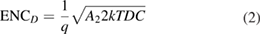
where q is the electric charge, A2 is a constant depending on the type of signal shaping (assumed here to be 1.18 [31]), k is the Boltzmann constant, D is the dielectric dissipation factor, and C is the capacitance [17].
From figure 11, the constant equivalent noise at ⩾80 V demonstrates that was no significant contribution from incomplete charge collection noise in this bias condition because there was no reduction in the combination as the bias was increased beyond 80 V. As such, the quadratic sum in these conditions can be said to be solely composed of dielectric noise, which is independent of bias and shaping time.
Given these statements, for each spectrometer separately, it is possible to consider any small apparent variations in dielectric noise which may occur with varied shaping time, as arising from repetition in measurement of the same physical quantity rather than real physical differences in dielectric noise—so long as each detector is reverse biased at ⩾80 V. This then provides six measurements at each reverse bias ⩾80 V of the same dielectric noise for each spectrometer. There are six measurements because six shaping times were used. These six measurements, the computed dielectric noises, for a 217 μm diameter photodiode (D2) and a 409 μm diameter photodiode (D4) at reverse bias of 80 V and 100 V, respectively, are shown in figure 12.

Figure 12. Computed dielectric noises as a function of shaping time for the 217 μm diameter photodiode spectrometer D2 (solid triangles and open triangles at reverse bias of 80 V and 100 V, respectively) and 409 μm diameter photodiode spectrometer D4 (solid squares and open squares at reverse bias of 80 V and 100 V, respectively).
Download figure:
Standard image High-resolution image
Since the dielectric noises of D2 spectrometer, ENCDT217, and D4 spectrometer, ENCDT409, each consist of the dielectric noises of their respective detectors (ENCD217 for 217 μm photodiode and ENCD409 for 409 μm photodiode), and some other system dielectric noise which is common between both spectrometers, the dielectric dissipation factor (see equation (2)) of Al0.52In0.48P can be estimated. First, the common system dielectric noise, ENCDx, must be considered; it is given by,

where all terms have been previously defined.
Following this, since the variation in the dielectric noise between the detectors themselves is solely due to the difference in their capacitances (equation (2)), the relationship between ENCD217 and ENCD409 can be expressed as,
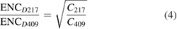
where C217 and C409 are the capacitances of the 217 μm diameter photodiode (0.72 pF and 0.67 pF at reverse bias of 80 V and 100 V, respectively) and 409 μm diameter photodiode (2.68 pF and 2.50 pF at reverse bias of 80 V and 100 V, respectively), respectively.
Thus, by combining equations (2)–(4), and considering all the data at 80 V and 100 V, the dielectric dissipation factor of Al0.52In0.48P was estimated to be (2.2 ± 1.1) × 10−3. This value is smaller than that reported for In0.5Ga0.5P (6.5 × 10⁻³) [12] but larger than Si (0.8 × 10⁻³) [15], GaAs (0.1 × 10⁻³) [32], and 4H-SiC (3.4 × 10⁻⁵) [33].
In a feedback resistorless charge-sensitive preamplifier the current of the detector in part sets the bias of the forward biased input JFET [23], which in turn influences the JFET's capacitance. The above determination is predicated on the assumption that the variations in detector leakage current between the 217 μm and 409 μm diameter photodiodes and in operating the detectors at biases of 80 V and 100 V, is sufficiently small that the capacitance of the JFET is not substantially changed. Given the low leakage currents of the detectors (<3 pA), it is believed that the assumption is valid.
4. Conclusions and further work
The results of the electrical characterisation of four Al0.52In0.48P mesa x-ray photodiodes with 6 μm thick i layers and two different diameters (217 μm ± 15 μm and 409 μm ± 28 μm) have been reported. The photodiodes were operated at room temperature (24 °C). Measurements of capacitance as functions of applied reverse bias showed similar capacitances between photodiodes of the same diameter. The capacitances of the four photodiodes decreased with the increased applied reverse bias, at the highest investigated bias (100 V), the capacitances of the 217 μm diameter and the 409 μm diameter photodiodes were found to be 0.7 pF and 2.5 pF, respectively. Being able to full deplete these devices demonstrates that residual doping in the i layer is not limiting the achievable depletion width in the Al0.52In0.48P material reported here. As such, it may be that thicker Al0.52In0.48P structures can be grown and also operated at full depletion. Greater depletion widths in thicker devices would result in greater quantum efficiencies; high quantum efficiencies are desirable for low flux environments and also extend the useful energy range of the detectors to harder (higher) energies. The measured leakage currents of both photodiodes were found to be <3 pA (corresponding to leakage current densities <2 nA cm−2) at 100 V reverse bias (corresponding to electric field strengths of 167 kV cm−1).
The performance of these photodiodes as photon counting spectroscopic x-ray detectors was investigated by connecting the photodiodes to a custom-made low-noise charge-sensitive preamplifier and illuminating them with an 55Fe radioisotope x-ray source. The best energy resolutions (FWHM at 5.9 keV) obtained were 0.89 keV and 1.05 keV with the 217 μm and 409 μm diameter devices, respectively. To achieve this both detectors were reverse biased at 100 V. The detectors and readout electronics were operated at room temperature. No significant contribution from incomplete charge collection noise was found at reverse biases ⩾80 V, thus the present detectors' thickness is not limiting charge collection. This promising result also encourages investigation of even thicker Al0.52In0.48P detectors; the quantum efficiency can be increased without incomplete charge collection adversely affecting the energy resolution. At the highest investigated reverse bias (100 V), the main limitation in the energy resolution of both spectrometers was due to the total capacitance at the input of the preamplifier induced noise (e.g. series white noise including induced gate current noise, 1/f series noise, and the dielectric noise).
Assuming the difference in the dielectric noise between the two spectrometers was only due to the different capacitances of the photodiodes, the dielectric dissipation factor of Al0.52In0.48P was estimated for the first time; a value of (2.2 ± 1.1) × 10−3 was found.
The results reported here demonstrate that Al0.52In0.48P photodiodes are promising devices for x-ray detection and spectroscopy. Such detectors are required for space science (e.g. analysis of planetary surfaces via x-ray florescence spectroscopy; monitoring of solar x-rays) and harsh terrestrial environment applications (e.g. in situ monitoring of tribological wear in oil lubricated machinery [34]; monitoring of nuclear material). Future work on these photodiodes will include investigating their characteristics at high temperatures (>30 °C) and in response to illumination with different radiations.
Acknowledgments
This work was in part supported by the Science and Technologies Facilities Council, UK, through grant ST/P001815/1 (University of Sussex, A M B, PI) and the Engineering and Physical Sciences Research Council, through grant EP/P021271/1 (University of Sussex, A M B, P I). A M B acknowledges funding received from The Leverhulme Trust, UK, in the form of a 2016 Philip Leverhulme Prize. The authors are grateful to R J Airey and S Kumar at the EPSRC National Epitaxy Facility for device fabrication.
Authors' Data Statement
Data underlying this work are subject to commercial confidentiality. The authors regret that they cannot grant public requests for further access to any data produced during the study.