

Abstract
Microwave-absorbing materials with light weight and high efficiency are desirable in addressing electromagnetic interference (EMI) problems. Herein, a nickel–cobalt sulfide (NCS) nanostructure was employed as a robust microwave absorber, which displayed an optimized reflection loss of −49.1 dB in the gigahertz range with a loading of only 20 wt% in an NCS/paraffin wax composite. High electrical conductivity was found to contribute prominent conductive loss in NCS, leading to intense dielectric loss within a relatively low mass loading. Furthermore, owing to its high electrical conductivity and remarkable dielectric loss to microwaves, the prepared NCS exhibited excellent performance in EMI shielding. The EMI shielding efficiency of the 50 wt% NCS/paraffin composite exceeded 55 dB at the X-band, demonstrating NCS is a versatile candidate for solving EMI problems.
Export citation and abstract BibTeX RIS
1. Introduction
With the rapid increase in the use of telecommunications, digital systems and fast processors, electromagnetic interference (EMI) problems have caused considerable concern since they impact almost all electric and electronic systems, from those used in daily life to those used in military activity and space exploration [1–4]. Microwave-absorbing materials, which attenuate electromagnetic energy in the gigahertz range by converting it into heat, are considered as promising candidates to address this issue. Currently, commercial microwave absorbents are typically composed of magnetic materials, such as ferrites and magnetic metals (nickel, cobalt and iron), which suffer from high density and instability at elevated temperatures [5–10]. Low-dimensional carbon nanomaterials, such as carbon nanotubes, are also considered as promising microwave absorbers with their intense dielectric loss and light weight [11, 12]. However, the large-scale application of these carbon-based nanomaterials is hindered by their relatively high cost compared with that of other inorganic materials. Therefore, it is urgent to explore novel microwave-absorbing materials that are stable, low-density and highly efficient.
Remarkable progress has been achieved in fabricating high-performance microwave absorbers by introducing nanostructured oxides, such as zinc oxides [13, 14], manganese oxides [15, 16], nickel oxides [17, 18] and cobalt oxides [19, 20], which can endure more rigorous environments than magnetic materials. Generally, the mechanism by which microwaves are attenuated in these oxides is dielectric loss caused by various polarization and relaxation processes [21]. However, the loss tangent (tanδε), a descriptor of the ability for microwave attenuation, is relatively low for these oxides due to the lack of a prominent resonance behavior throughout the gigahertz range compared with magnetic materials. Hence, the mass loading of the oxides is relatively high when they mix with paraffin wax (~50 wt%) in the measurements, which hinders their application as light and highly efficient microwave absorbers [15, 22, 23]. To enhance the attenuation efficiency of microwave absorbers, nanomaterials with multiple components and complex morphology have been employed, including CoNi@SiO2@TiO2 microspheres [3], γ-Fe2O3@C@α-MnO2 nanospindles [5], yolk–shell Ni@SnO2 composites [10], graphene@Fe3O4@SiO2@NiO structures [17] and FeCo/C/BaTiO3 nanocomposites [23]. Although favorable microwave absorption performance has been achieved, the widespread application of these examples is hindered by their complicated procedures in the synthesis process.
Generally, the mechanism by which microwaves are attenuated in dielectrics is dominated by either polarization loss or conductive loss [24]. Recent studies highlight that conductive loss in nanostructured metal oxides can be promoted by creating micro-circles in samples, resulting in enhanced microwave absorption [13, 15, 25]. In particular, mixed-valence transition metal oxides, for instance NiCo2O4, display significant conductive loss as well as superior microwave absorption properties compared with their corresponding unitary oxides [26, 27]. These emergent results imply that high-efficiency microwave-absorbing materials can be realized by regulating their conductive loss via rational design and fabrication. Herein, we present a nickel–cobalt sulfide (NCS) nanostructure for a novel microwave-absorbing material, which manifests remarkable conductive loss in the microwave range, and displays a reflection loss of −49.1 dB with a loading of only 20 wt% in the NCS/paraffin composite. Interestingly, we found that with increased mass loading, the NCS/paraffin composite shows excellent EMI shielding performance. The EMI shielding efficiency (SE) of a 50 wt% NCS/paraffin composite exceeds 55 dB through the tested frequency, demonstrating multifunctional applications for NCS in addressing EMI problems.
2. Experimental
2.1. Synthesis of NCS nanostructures
A Ni–Co layered double hydroxide (LDH) precursor was synthesized via the hydrothermal method described in our previous work [28]. In a typical synthesis of NCS, a 30 mg Ni–Co LDH precursor was re-dispersed in 20 ml ethanol, followed by dissolving 50 mg thioacetamide (TAA) under vigorous stirring for 30 min. The suspension was transferred into a 46 ml Teflon-lined stainless-steel autoclave and kept at 180 °C for 6 h, during which the hydroxide precursor was sulfurized by TAA. The product was washed by ethanol several times and vacuum-dried at 60 °C for 8 h to obtain 3D-structured NCS. As a control, a NiCo2O4 (NCO) nanomaterial was prepared by annealing the same Ni–Co LDH precursor in a tube furnace at 400 °C for 8 h with air flow to convert the hydroxide precursor into a spinel-structured nickel–cobalt oxide.
2.2. Characterization
Powder x-ray diffraction (XRD) data were obtained on a Shimadzu XRD-7000 powder x-ray diffractometer with monochromatized Cu Ka irradiation. Field-emission scanning electron microscopy measurements were made on a Hitachi S4800 microscope. High-resolution transmission electron microscopy (HRTEM) and selected-area electron diffraction (SAED) were performed on a Tecnai G2 F30 S-TWIN instrument at an accelerating voltage of 300 kV, accompanied by energy-dispersive x-ray mapping for element distribution analysis. High-resolution x-ray photoelectron spectroscopy (XPS) measurements for evaluation of elemental species and their chemical states were carried out on a Thermo ESCALAB250Xi with a resolution of 0.43 eV. The current–voltage (I–V) curves were recorded by linear sweep voltammetry using a CHI 660E electrochemical workstation. The electrode was prepared by pressing the as-synthesized samples (20 mg) into a disk (d = 0.6 cm), and was sandwiched with two copper disks (d = 0.4 cm).
2.3. Electromagnetic parameter measurements
The electromagnetic parameters were recorded on an Agilent PNA-N5244A vector network analyzer after the samples were mixed with paraffin wax with controlled NCS mass loadings. To measure the relative permittivity and permeability, the mixtures were pressed into toroidal samples ( and
and  in diameter) and tested at the range of 2–18 GHz. The scattering parameters (S11, S22, S12, S21) of the samples were measured by the same network analyzer at the X-band frequency (8.2–12.4 GHz). The composites were cut into rectangular films with a thickness of 2 mm for measurements. The reflection (R) and transmission (T) coefficients were calculated based on the obtained scattering parameters:


The total EMI SE (EMI SET) is the sum of the contributions from reflection (SER) and absorption (SEA), and can be written as:

where SER and SEA can be expressed as
3. Results and discussion
The NCS was synthesized via a simple hydrothermal reaction by sulfurizing the Ni–Co LDH nanostructure with TAA. As shown in figures S1(a) and (b) (in the electronic supplementary material (ESM) (stacks.iop.org/JPhysD/51/235303/mmedia)), 3D NCS is obtained after sulfurization; the hierarchical morphology of the NCS is inherited from its precursor (figure S2(a) in the ESM). The diameter of the nanoflake-constituted nanostructures is about several micrometers, and the thickness of the nanoflakes is about 20–30 nm (figure S1(c) in the ESM). XRD characterization reveals that the crystalline structure of the sample (figure S1(d) in the ESM) can be indexed to NiCo2S4 (JCPDS 20-0782). HRTEM was employed to investigate the microstructure of NCS (figures 1(a)–(c)). Figure 1(a) shows a TEM image of a single NCS nanoflake isolated from its 3D structure. The HRTEM image of this nanoflake (figure 1(b)) shows well-resolved lattice fringes with interplanar d-spacings of 0.332 nm, corresponding to the (2 2 0) crystal plane of NiCo2S4. This is also proved by the SAED pattern in figure 1(c), which presents diffraction spots that index to the (2 0 2), (2 2 0) and (4 2 2) planes of spinel-structured NiCo2S4. We also conducted an elemental mapping measurement on the sample (figure 1(d)), in which Ni, Co and S are all observed to be distributed homogeneously, indicating the monophase nature of the sample and consistency with the XRD result. XPS measurements were made to investigate the variation in surface electron states of NCS, as shown in figures 1(e)–(g). The XPS spectra for both Ni 2p and Co 2p display well-resolved peaks of M2+ 2p3/2, M3+ 2p3/2, M2+ 2p1/2, and M3+ 2p1/2 (M = Ni, Co), indicating the coexistence of Ni2+, Ni3+, Co2+, and Co3+ species in the NCS nanostructure. The narrow peak width and minor satellites in the Ni 2p3/2 and Co 2p3/2 regions suggest the metallic nature of NCS [29], which might influence its properties in electromagnetic wave response profoundly.

Figure 1. (a) TEM, (b) HRTEM, (c) SAED pattern and (d) elemental mapping of NCS. XPS spectra of (e) Ni2p, (f) Co2p and (g) S2p of NCS.
Download figure:
Standard image High-resolution imageThe NCS nanostructure was mixed with paraffin wax with a controlled mass loading (10, 20, 30, and 40 wt%) to measure the relative permittivity ( ) and permeability (
 ) at 2–18 GHz. In general, the real part of permittivity (
 ) represents the ability of energy storage in the alternating electromagnetic field, whereas the imaginary part of permittivity (
 ) represents the ability of energy attenuation for a material. As shown in figures 2(a) and (b),
  of NCS declines gradually from 2–18 GHz, implying typical dielectric response characteristics. Both
  and
and  increase rapidly with the NCS concentration varying from 10 to 40 wt%. For the composite with 40 wt% NCS, the
  value is 87 at 2 GHz, while the
  value is as high as 217. These values are significantly higher than those of previously reported dielectric-based microwave absorbers at the same mass loading, indicating a sensitive responsivity to microwaves for NCS [8, 10, 12, 18, 30, 31]. Additionally, the
  and
and  values of NCS nearly remain constant at 1 and 0, respectively, (figure S5 in the ESM) revealing that magnetic loss is negligible throughout the tested frequency.

Figure 2. (a) Real and (b) imaginary parts of permittivity of NCS/paraffin wax composites with varied mass loading.
Download figure:
Standard image High-resolution imageThe reflection loss of NCS is calculated based on the measured complex permittivity and permeability according to the transmission line theory expressed as follows [32, 33]:

where f is the frequency of the electromagnetic wave, d is the thickness of the absorbent, c is the velocity of light, Z0 is the impedance of the free space, and ZIN is the input impedance of the absorbent. The calculated reflection loss of NCS with different mass loadings is presented in the 3D images in figure 3, which show the dependence of reflection loss on the coating layer thickness (1–6 mm) and the applied frequency (2–18 GHz). The NCS series show significant differences in microwave absorption, where the composite with 20 wt% NCS loading (NCS-20) exhibits the best performance. The optimized reflection loss of −49.1 dB is obtained at the frequency of 5.9 GHz with a thickness of 1.7 mm. Meanwhile, the effective bandwidth for microwave absorption of NCS-20 ranges from 5.5 to 18 GHz when the thickness of the absorber is varied from 1.5 to 3.5 mm, exhibiting a remarkable wideband absorption property. It is noted that larger  and
and  values do not result in better microwave absorption in this study. This is due to the impedance match requirement for microwave absorbents: large
  and
and  values can attenuate microwave energy rapidly, but lead to increased microwave reflection at the air–material interface where the incident microwave is hindered [24]. Therefore, for a dielectric absorbent without magnetic loss, excellent microwave absorption is likely to be obtained from absorbents with moderate
  and
and  values. For NCS-20,
  declines from 15.6 to 9.4 along with the frequency, while
  varies between 4.0 and 8.9, which satisfy the impedance match requirement for microwave absorption. Considering that the optimized concentration of NCS in the NCS/paraffin wax composite is as low as 20 wt%, this study presents a light-weight microwave absorbent with attractive performance and a cost-effective fabrication route. A comparison of concentration-dependent performance between recently reported results and our work is shown in table 1.
Table 1. Comparison of the concentration-dependent performance between recently reported results and our work.
| Filler | Matrix | Concentration | Thickness (mm) | Reflection loss (dB) | Ref. |
|---|---|---|---|---|---|
| CoNi@SiO2@TiO2 | EP | 25 wt% | 2.1 | −58.2 | [3] |
| NiCoZn ferrite/graphene | Paraffin | 40 wt% | 3.1 | −53.5 | [6] |
| NiFe2O4/r-GO | Paraffin | 70 wt% | 5.0 | −42 | [7] |
| 3D nickel chains | SiO2 powder | 50 wt% | 1.8 | −50 | [9] |
| Ni@void@SnO2 | Paraffin | 50 wt% | 1.5 | −50.2 | [10] |
| ZnO nanostructures | Paraffin | 50 vol% | 5.0 | −42 | [13] |
| MnO2 nanostructures | Paraffin | 50 wt% | 1.9 | −41 | [15] |
| Graphene@Fe3O4@SiO2@NiO | Paraffin | 25 wt% | 1.8 | −51.5 | [17] |
| NiO@graphene | Paraffin | 25 wt% | 1.7 | −59.6 | [18] |
| Co@CoO | Paraffin | 50 wt% | 1.3 | −90.2 | [19] |
| CoO nanostructures | EP | 17 wt% | 2.0 | −37 | [20] |
| BaTiO3 nanotubes | Paraffin | 70 wt% | 2.0 | −21.8 | [22] |
| Ti2CTx MXene | Paraffin | 55 wt% | 2.1 | −50.3 | [24] |
| Hierarchical NiCo2O4 | Paraffin | 50 wt% | 4.0 | −25.5 | [25] |
| MoS2 nanospheres | PVDF | 25 wt% | 2.5 | −26.11 | [30] |
| PEDOT–RGO–Co3O4 | Paraffin | 50 wt% | 2.0 | −51.1 | [33] |
| NiCo2S4 nanostructure | Paraffin | 20 wt% | 1.7 | −49.1 | This work |
EP: Epoxy resin. PVDF: Polyvinylidene fluoride.
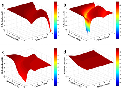
Figure 3. Reflection loss of NCS/paraffin wax composites with mass loading of (a) 10%, (b) 20%, (c) 30% and (d) 40%.
Download figure:
Standard image High-resolution imageTo demonstrate the outstanding microwave absorption properties of NCS, the reflection loss of NCO was also investigated as a control. NCO was converted from the same Ni–Co LDH precursor. The morphologies of NCO and NCS are thus identical to each other, which otherwise would be an additional factor affecting the performance comparison (figure S2 in the ESM). As shown in figures 4(a) and (b), the maximum reflection loss of NCO is −15.4 dB at a thickness of 1.5 mm, which is −18.2 dB lower than that of NCS at the same thickness, and −32.0 dB lower than the optimal value of NCS. This result shows that the excellent microwave absorption performance of NCS can be attributed mainly to its intrinsic properties rather than other factors such as the morphology of the materials. To understand the difference in microwave absorption between NCS and NCO, the relative permittivity and permeability of the two samples are presented in figures 4(c) and (d). The  of NCS is higher than that of NCO throughout the whole tested frequency, while the
  of NCS is lower than that of NCO at most of the frequency (from 4.6 to 18 GHz). As a result, the loss tangent (
 ) of NCS is significantly larger than that of NCO with the frequency increasing from 2–18 GHz. The maximum tanδε of NCS is 0.57 at 2 GHz, which is larger than those of most reported nanomaterials, demonstrating the potent microwave loss property of NCS [13–20]. Furthermore, the locations of the resonance peaks from NCS and NCO are similar to each other, implying that the same polarization processes occurred in the two samples.

Figure 4. Comparison of microwave absorption performance between NCS and NCO. Reflection loss of (a) NCS and (b) NCO with mass loading of 20 wt%. Comparison of (c) complex permittivity and (d) dielectric loss tangent between NCS and NCO.
Download figure:
Standard image High-resolution imageFurther study is dedicated to probing the microwave loss mechanisms of NCS nanostructures. According to the Debye equation, the  and
and  values for a dielectric material are expressed as follows [34, 35]:
where  is the static frequency (
 ),
),  is the permittivity at infinite frequency (
 ),
),  is the angular frequency (
 ), and
  is the relaxation time of dipoles. Combining equations (8) and (9), the relationship between
  and
and  can be expressed as:
In equation (10), the relaxation time  depends on the type of dielectric loss. In the case where dielectric loss is associated with only one physical phenomenon, the curve of
  versus
  should be a straight line. Therefore, the relaxation time for a polarization process can be obtained by calculating the slope of the line (
 ), in which
  is a constant. In this study, we observed three straight lines fitted from the
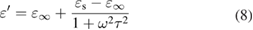
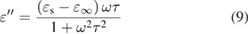
  curves for both NCS and NCO (figures 5(a) and (b)), which imply several types of polarization with their own independent relaxation times at the testing frequency. The result also shows that the polarization processes in NCS and NCO are similar to each other, which is consistent with the analysis presented above. It also indicates that polarization and relaxation processes are not responsible for the difference in dielectric loss between NCS and NCO.
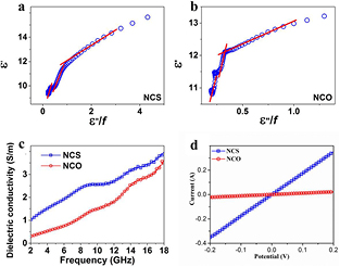
Figure 5. The plots of  versus
  for (a) NCS and (b) NCO. (c) The dielectric conductivity of the samples based on equation (3), and (d) I–V curves of NCS and NCO.
Download figure:
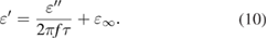
Standard image High-resolution imageOn the other hand, dielectric conductivity was also investigated to explore the enhanced dielectric loss of NCS. Conductive loss refers to the microwave energy attenuation caused by the movement of charge carriers in absorbents, which depends on the dielectric conductivity of the samples, and is expressed as follows [24, 34]:

where σ is the dielectric conductivity, and ε0 is the permittivity of free space. The dielectric conductivity versus frequency of NCS and NCO are shown in figure 5(c). It can be observed that the dielectric conductivity of both samples increases along with the frequency. The dielectric conductivity of NCS is higher than that of NCO at the whole tested frequency, exhibiting a greater ability for charge transfer for NCS. This is caused by the metallic nature of NCS, which is supposed to deliver high electrical conductivity. To confirm this, the samples of NCS and NCO were pressed into a circular plate to probe their I–V characteristics. As shown in figure 5(d), the slope of the I–V curve for NCS is remarkably steeper than that for NCO, revealing a higher electrical conductivity of NCS. Previous work has also revealed the metallic nature of first-row transition-metal-based sulfides, experimentally and theoretically [36]. Therefore, the robust conductive loss of NCS can be attributed to its high dielectric conductivity, and leads to potent microwave absorption performance with a low mass loading.
In addition to microwave absorption, one approach to addressing EMI problems is shielding. An effective EMI shielding material is typically supposed to be either one that is electrically conductive and can directly reflect radiation by the interaction between the charge carriers and microwave, or one that is able to absorb electromagnetic radiation by the interaction between the microwave and the material's electric and/or magnetic dipoles [1]. At present, the EMI shielding materials used commercially are metal shrouds, which are less desirable due to their susceptibility to corrosion [37–39]. Herein, inspired by the high electrical conductivity and dielectric loss, we investigated the possible application of NCS nanostructures as EMI shielding material. We prepared NCS/paraffin wax films with different NCS mass loadings and a thickness of 2 mm to probe the scattering parameters at the X-band, from which the EMI SE of NCS was obtained.
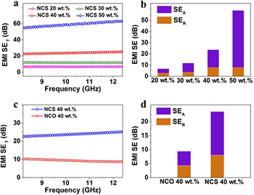
As shown in figure 6(a), the EMI SE of NCS increases along with the NCS loading. For instance, the average EMI SE of the 30 wt% NCS composite is 11.7 dB, indicating that more than 90% of the microwave energy has been blocked by the shielding layer. As the NCS loading rises to 50 wt%, an average EMI SE higher than 55 dB is obtained at the tested frequency, which indicates only 0.0003% transmission through the shielding layer. In general, the total EMI SE (SET) comprises the reflection SE (SER) and absorption SE (SEA), as expressed in equation (3). To investigate the shielding mechanisms of NCS composites, the contributions of SER and SEA are plotted in figure 6(b). With rising NCS content, SEA increases rapidly, while SER no longer upswings after NCS loading reaches 40 wt%. For the NCS 50 wt% composite, SEA and SER are 50.5 dB and 8.1 dB, respectively, showing that shielding due to absorption rather than reflection is the dominant mechanism in NCS composites. The absorption mechanism of EMI shielding includes the absorption of electromagnetic radiation due to the material's dielectric and/or magnetic loss triggered by the radiation, and internal reflections arising from scattering centers and interfaces within the shielding material [1]. It is demonstrated above that the NCS composite exhibits intense dielectric loss in microwave frequencies. Moreover, highly efficient reflection and scattering is achieved because of the rich free electrons at the surfaces and interfaces of the highly conductive NCS. To verify this, the EMI SE of NCO with the same mass loading was studied. As shown in figure 6(c), the average EMI SE of the NCO 40 wt% composite is less than 10 dB at the X-band, in contrast to the higher than 20 dB EMI SE of the NCS composite with the same mass loading. Significant differences originating from both SEA and SER are observed in figure 6(d), further demonstrating that the outstanding EMI shielding performance of NCS can be attributed to the synergistic effects of its intense dielectric loss and high electrical conductivity.
Figure 6. (a) EMI SE in the X-band of the NCS/paraffin wax composites with varied mass loading of NCS. (b) Average values of SEA and SER for NCS/paraffin wax composites with varied mass loading of NCS. Comparison of (c) EMI SE and (d) SEA and SER values between NCS and NCO at 10 GHz.
Download figure:
Standard image High-resolution image
4. Conclusion
In summary, we have shown here that hierarchical NiCo2S4 nanomaterials display excellent performance both in microwave absorption and in EMI shielding. Owing to its high electrical conductivity, NCS contributes a remarkable dielectric loss in the microwave range, leading to an optimized reflection loss of −49.1 dB with loading of only 20 wt%. Moreover, NCS exhibits a potent capability for EMI shielding: an EMI SE higher than 55 dB is achieved with the NCS 50 wt% composite at the X-band. This work provides promising candidates for fabricating highly efficient and durable microwave absorbents and EMI shielding materials, and paves the way for the application of a large family of transition metal sulfides in addressing EMI problems.
Acknowledgments
The authors acknowledge the financial support provided by the National Natural Science Foundation of China (Nos. 61301026, 815680487), the Postgraduate Research and Practice Innovation Program of Jiangsu Province (XKYCX17_031), and the Yangzhou University International Academic Exchange Fund. We also appreciate the technical support from the Testing Center of Yangzhou University.