
Abstract
The family of hybrid organic–inorganic halide perovskites is in the limelight because of their recently discovered high photovoltaic efficiency. These materials combine photovoltaic energy conversion efficiencies exceeding 22% and low-temperature and low-cost processing in solution; a breakthrough in the panorama of renewable energy. Solar cell operation relies on the excitation of the valence band electrons to the conduction band by solar photons. One factor strongly impacting the absorption efficiency is the band dispersion. The band dispersion has been extensively studied theoretically, but no experimental information was available. Herein, we present the first experimental determination of the valence band dispersion of methylammonium lead halide in the tetragonal phase. Our results pave the way for contrasting the electronic hopping or the electron effective masses in different theories by comparing to our experimental bands. We also show a significant broadening of the electronic states, promoting relaxed conditions for photon absorption, and demonstrate that the tetragonal structure associated to the octahedra network distortion below 50 °C induces only a minor modification of the electronic bands, with respect to the cubic phase at high temperature, thus minimizing the impact of the cubic-tetragonal transition on solar cell efficiencies.
Export citation and abstract BibTeX RIS

Original content from this work may be used under the terms of the Creative Commons Attribution 3.0 licence. Any further distribution of this work must maintain attribution to the author(s) and the title of the work, journal citation and DOI.
Invited by Board Member Patrick Soukiassian
1. Introduction
Organic–inorganic halide perovskites are disrupting materials of photovoltaics nowadays, due to their strong light absorption ability, coupled with the easiness and low cost of the fabrication process in solution [1–3]. Their performance in solar cells has raised spectacularly in only few years above 22% [1, 3–12], almost to the level of silicon cells, the most widely used commercial technology [13]. Methylammonium triiodideplumbate (CH3NH3PbI3, MAPbI3 or MAPI) currently exhibits the highest solar energy conversion rate and carrier diffusion lengths above 1 µm [14, 15], so the same material could fulfill both the absorbing and transport functions of the solar cell. The photovoltaic efficiency of MAPI, as in all the compounds of the hybrid perovskite family, has been phenomenologically studied without an experimental determination of the band structure. The precise details of the band structure are, however, extremely important. They can explain the band gap value and therefore the absorbed photon energies, the nature of the band gap (direct or indirect) associated with the photon absorption efficiency and the effective masses of charge carriers in the material, relevant for the charge transport to the electrodes.
Theoretical calculations provide invaluable information for these questions and therefore the electronic structure of hybrid perovskites has been intensively studied both on static structures [16–26] and in models including the dynamical reorientation of organic cations [27–32]. The effective mass of charge carriers has also been studied, and the predictions differ by a factor of two [19, 23, 33, 34]. This wealth of theoretical studies needs to be compared to an experimental study, as contrasting theory and experiment allows for a more accurate modeling of the electronic structure or may even lead to unexpected discoveries. For instance, in long studied systems like h-BN, there are controversies about basic issues of the electronic band structure; while theories predict an indirect band gap, photoluminescence experiments provide evidence instead of a direct band gap 1.6 eV [35–37]. Valuable information on the experimental density of states of hybrid perovskites has already been gathered in angle-integrated photoemission [17, 38–40]. However, the experimental band dispersion has remained elusive.
Herein, we present the first experimental determination of the valence band dispersion of MAPI, thanks to our angle-resolved photoemission experiments. The band structure shows an apparent electronic periodicity that does not correspond to the expected structural periodicity from the tetragonal phase, but to the periodicity of the high temperature cubic phase. The tetragonal distortion of the octahedra induces an almost non-appreciable change of the electronic properties, implying that the impact of the tetragonal-cubic transition on the operation of solar cells should be minor. Moreover, the comparison of our experimental determination of the band structure with existing calculations suggests the necessity of introducing renormalization factors of the energy for some bands.
2. Methods
2.1. Sample growth
Hybrid perovskites are prepared in a two-step process. First, the organic and inorganic precursors are diluted in the solvent. Afterwards, the solvent is evaporated and the precursors self-assemble into the hybrid perovskite. Depending on the precursor stoichiometry and the nature of the organic moiety, self-assemblies with different dimensionalities appear (3D, 2D...).
MAPI perovskite is synthesized from PbI2 and methylammonium iodide  . When the solvent evaporates, the reaction giving rise to the perovskite is:

Formerly, it was necessary to obtain  from methylamine according to the reaction:

In our case, we pour drop by drop 17.2 ml of HI (57% stabilized) on 15 ml of cold methylamine. The mixture is agitated during 2 h. Methanol from the solution is evaporated in a rotary evaporator at 60 °C during 1 h. The aqueous solution is then poured in diethylether to precipitate the methylammonium iodide salt  . The precipitation is filtered and washed with diethylether to remove any traces of I2. The salt is then recrystallized in ethanol. Once the methylammonium iodide salt is dried after baking at 60 °C overnight, the solution is ready to be prepared.
We prepare a solution of 40% PbI2 in mass in gamma-butyrolactone (GBL) with one equivalent of  . The solution is stirred at 60 °C during 8 h to dilute PbI2. Once the solution is limpid, the solvent is evaporated at 100 °C to self-assemble the hybrid perovskite.
2.2. X-ray diffraction experiments
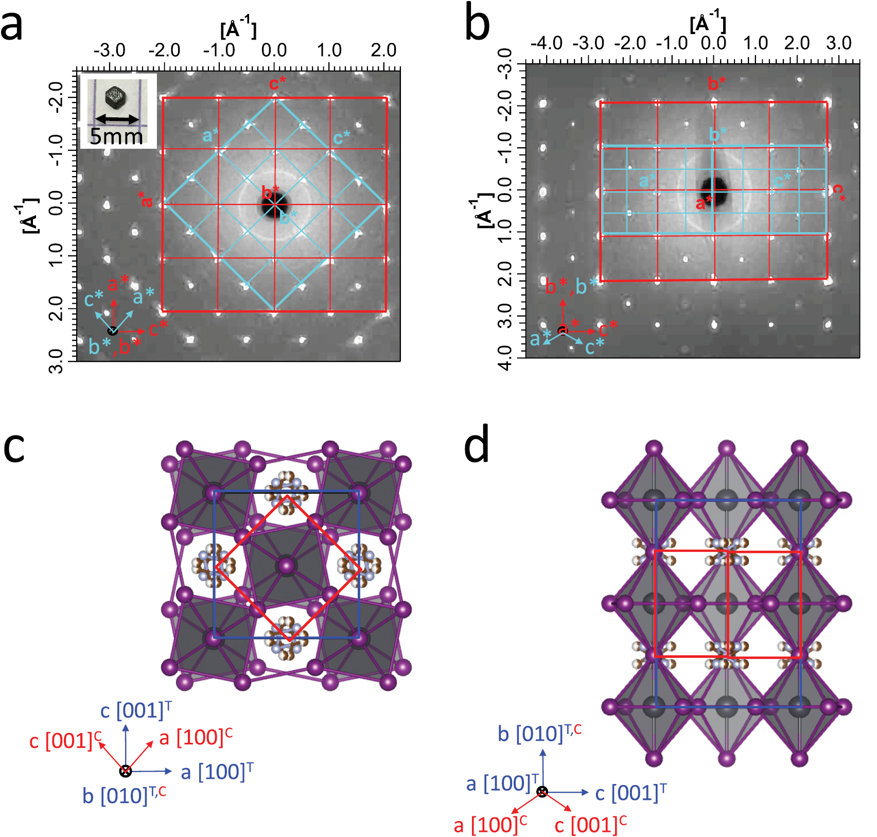
The above sample growth procedure gives rise to monocrystals up to the millimetric size (see the inset in figure 1(a)). The monocrystallinity is explicit in the diffraction pattern being constituted by spots and not circles. Monocrystal x-ray diffraction experiments were performed at the CRISTAL beamline of synchrotron SOLEIL by using a four-circle diffractometer equipped with a 2D detector. Photons of λ = 0.4367 Å were selected by a Si(1 1 1) crystal. The temperature was 200 K. CrysAlisPro software was used for indexing the reflections. The structures were solved by direct methods using the SHELX package [41] under WinGX interface [42]. The positions were initially refined isotropically. Anisotropic displacements were introduced in the second step of the refinement.

Figure 1. X-ray diffraction measurements of MAPI hybrid perovskite monocrystals in the tetragonal LT phase. Reciprocal space as measured by x-ray diffraction in the (a) (h 0 l) and (b) (0 k l) planes at 200 K. The projected reciprocal unit cells for the tetragonal periodicity are indicated in blue. The cubic reciprocal unit cell is also displayed for comparison. Refined structure of MAPI at 200 K from our data (tetragonal I4/mcm) projected on (c) the ac plane and (d) on the bc plane (see supplementary data for the details of the structural results). In the tetragonal structure, a distortion of the octahedra lattice promotes a larger unit cell (in blue) with respect to the cubic one (in red). The crystallographic directions are indicated by the tetragonal (T) and cubic (C) lattice vectors.
Download figure:
Standard image High-resolution image2.3. ARPES experiments
The freshly grown samples were cleaved in situ under ultrahigh-vacuum conditions by gluing a post on the sample, which was hit with a wobble stick. ARPES measurements were carried out at the CASSIOPEE beamline of SOLEIL synchrotron. Sample homogeneity was checked spectroscopically by checking both the core levels and the valence band. The beamline is equipped with a high-resolution modified Petersen grating monochromator with a resolution E/ΔE ≃ 25 000 below 100 eV. The analyzer is a Scienta R4000 detector with resolution ΔE < 1 meV and Δk ~ 0.01 Å−1 at hν = 36 eV. Binding energies are referenced to the Fermi level of a metal in electrical contact with the sample. The sample temperature was 170 K.
3. Results and discussion
The first requirement to measure the band structure with k-resolution is to obtain large monocrystals, because polycrystals allow us to determine only the density of states, due to the averaging of differently oriented crystallites. Our preparation method gives rise to millimetric monocrystals as suggested by observation from the naked eye (inset in figure 1(a)) and demonstrated by x-ray diffraction. The reciprocal space as measured by x-ray diffraction in the (h 0 l) and (0 k l) planes at 200 K is shown in figures 1(a) and (b), also indicating the projection of the reciprocal unit cells of the tetragonal structure (blue). Thin Bragg reflections are observed without a trace of rings, proving the absence of pollycrystalline powder in our crystal. Our x-ray diffraction data are a complete set, allowing the structural refinement of the structure. We thus confirm the expected tetragonal structure at 200 K [18, 43], with lattice parameters a = 8.80 Å, b = 12.68 Å and c = 8.80 Å. Our resulting structure is shown in figures 1(c) and (d) and the final atomic positions, as well as the details of the structural determination, are found in the supplementary data (stacks.iop.org/JPhysD/50/26LT02/mmedia).
Measuring the band structure with k-resolution is therefore possible in these monocrystals, and can be determined by angle-resolved photoemission. The band structure determination of a 3D system requires carefulness, as the bands are expected to disperse with respect to the k perpendicular to the surface, i.e. with respect to the photon energy. The first step is thus to determine the appropriate photon energy of a high symmetry plane of the Brillouin zone. Synchrotron radiation is therefore the only possibility for appropriately measuring the band structure in a 3D system. Figures 2(a) and (b) show our analysis of the band structure as a function of the photon energy. In panel (a), E(k) measurements of the photoemitted intensity along the a direction, containing normal emission for three photon energies, are shown. The higher intensity reveals different electronic states that evolve when hν is varied, i.e. that disperse with k perpendicular to the surface. The dispersion is more evident when a whole set of measurements is performed and the electronic structure at a given binding energy is presented, preferentially at energies associated with a particular electronic state. Figure 2(b) presents such a constant energy cut. Here ky corresponds to the dispersion perpendicular to the surface, while kx corresponds to a dispersion parallel to the surface. At this stage, it is not yet possible to identify whether this corresponds to a high symmetry direction or not. It is immediately appreciated in this constant energy cut that the photoemitted intensity changes with ky, with a maximum intensity in the center of our ky range and an intensity decrease at the edges. This detection range does not show several periods of the intensity evolution. However, it is larger than 1.0 Å−1, the biggest relevant Q vector that can appear in the system, and the one related to a cubic unit cell with a single PbI6 octahedron (red line in figure 2(b)). This region of the reciprocal space is wide enough to identify the high symmetry planes of the electronic structure, as the mirror planes of the photoemitted intensity in figure 2(b). In particular, the photon energy of 118 eV and 142 eV correspond to the maximum and the minimum intensity along ky and can be used to explore one of the high symmetry planes of the electronic structure.

Figure 2. Electronic dispersion as a function of the photon energy and electronic periodicity in the tetragonal LT phase. (a) Photoemission measurements along a direction containing the normal emission for different photon energies. Arrows highlight the evolution of different electronic states. Such an evolution corresponds to the electronic states dispersing perpendicularly to the surface, as expected for a 3D material. The dispersion is also explicit in the intensity variation of the constant energy cuts of the electronic structure, both (b) out-of-plane (2340 meV below the VBM for photon energies 74 eV < hv < 200 eV) and for (c) in-plane (VBM at hv = 130 eV). (b) is the lattice vector perpendicular to the surface in the usual convention for this structure. The size of the lattice vectors for the cubic (red, C) and tetragonal structures (blue, T) are indicated. The spectral weight seems to follow the cubic periodicity.
Download figure:
Standard image High-resolution imageWhen doing this analysis, we also observe that the photoemitted intensity in the constant energy cut does not correspond to the tetragonal periodicity (blue line in figure 2(b)), as expected at 170 K. The photoemitted intensity seems to instead have a periodicity along ky of 1 Å−1, corresponding to the cubic periodicity or to a tetragonal phase with the b axis parallel to the surface. We have therefore fixed the photon energy at 130 eV to explore the photoemitted intensity parallel to the surface (figure 2(c)). Again, the tetragonal lattice parameter is too small to reproduce the experimental features, and the cubic lattice parameter better describes the characteristic size of the spectral features. As both the parallel and perpendicular spectral features have the characteristic size of the cubic periodicity, we conclude that the electronic properties seem to exhibit a cubic symmetry, even at temperatures corresponding to the tetragonal phase. We will later discuss this phenomenon, but, in any case, we can already identify the high symmetry planes of the electronic structure. We therefore use, in the following, 142 eV corresponding to the minimum intensity along ky, i.e. the ΓXM plane.
Figure 3(a) shows the Brillouin zone of the cubic system and highlights the ΓMX plane where the band structure has been determined. Figure 3(b) shows a sketch of the expected bands at this plane. The maximum of the valence band is at M, while at slightly deeper binding energies, the bands disperse down in the MX direction. The highest intensity at the valence band maximum allows us to identify an M point (figure 3(c)). Other M points do not reach the same intensity, due to the photoemission matrix elements. Matrix elements can prevent the photoemitted intensity of exhibiting clearly the periodicity of the electronic states [44, 45]. When increasing the binding energy by 300 meV, some intensity also develops at the X points, as expected (figure 3(d)). This preliminary orientation can be confirmed by studying the deeper I 5p and Pb 6s bands, whose minimum is reached at Γ (figure 3(f)). Figure 3(b) shows that at lower binding energies, the bands disperse in the XM direction, as observed in figure 3(e). This procedure allows us to identify the high symmetry directions.

Figure 3. Periodicity of the electronic structure of MAPI. (a) Cubic Brillouin zone. The highlighted red plane corresponds to the constant energy cuts further studied. (b) Sketch of the main expected bands in the ΓXM plane. Constant energy cut of the electronic structure in the ΓXM plane at a binding energy corresponding to (c) the maximum of the valence band, (d) 300 meV, (e) 2440 meV and (f) 2840 meV below the maximum of the valence band. The cubic Brillouin zones are highlighted as red squares. These constant energy cuts are indicated in panel (b) as colored planes. The stars indicate the expected intersection of the bands with these planes.
Download figure:
Standard image High-resolution imageIn order to determine the electronic structure along the high symmetry directions, we need to analyze the whole set of constant energy cuts that we have measured. However, experimental bands could be renormalized in energy, as observed in other systems [46, 47], rendering the comparison between the experiment and theory less direct. We thus need to figure out if bands are strongly renormalized or not. Figure 4(a) precisely shows the dispersion along the a direction out of a high symmetry direction, making explicit the presence of dispersing states. Some states are better appreciated when applying settled treatments of the photoemission data to the raw data of figure 4(a). In the first step, the normalization by the density of states [48] allows us to see dispersions hidden by a density-of-states-like intensity, due to phonon excitations. In this treatment, the low dispersing states, as the molecular states or the core levels, are minimized, although they are of course visible in the raw data. A second derivative treatment has then been performed on the data to better appreciate some dispersions (figure 4(b)), although our analysis does not rely on this data treatment.

Figure 4. Electronic structure of MAPI hybrid perovskite with k-resolution. (a) Photoemission measurement out of a high symmetry direction (hv = 142 eV) making explicit the presence of dispersing spectral features. (b) Second derivative of the data normalized to the density of states. (c) Valence band integrated in angle in several Brillouin zones and compared to theoretical calculations [25]. (d) Spectrum at normal emission in a wide binding energy range and its normalization by the density of states in (f). (e) Integrated valence band in (d) compared to theoretical calculations [25]. Reprinted with permission from [25], Copyright 2016 by the American Physical Society.
Download figure:
Standard image High-resolution imageIt can be appreciated in figures 4(a)–(c) that the experimental electronic states are concentrated on a small energy window of 3.5 eV from the valence band maximum (VBM). This energy range is better appreciated on an 'experimental density of states (DOS)', obtained by integrating the photoemission intensity of the constant energy cuts in several Brillouin zones (circles in figure 4(c)). When comparing the 'experimental DOS' to the calculated one (figure 4(c)), it is observed that the density of states is spread in a similar energy range between the VBM and −3.5 eV. This is also the case for different photon energies, as shown on wide energetic scans in figures 4(d) and (e). These experimental states can be identified through comparison to the calculations. The states between the VBM and −3.5 eV correspond to the antibonding in-plane σ bonds between I 5p and Pb 6s. Other peaks appear at higher binding energies, as observed in figure 4(f). The one at −6.6 eV is associated to the dispersiveless state of the organic cation and the one at −8.5 eV corresponds to the Pb 6s states and other molecular states.
Further information can be extracted from the band dispersions. Figure 5 shows the MΓM and the MXM directions of the cubic Brillouin zone, the raw data (figures 5(a) and (d)), the second derivative (figures 5(b) and (e)) and its comparison with the cubic band structure (figures 5(c) and (f)). In the theoretical bands along both directions, the highest dispersing band is the lowest one, which is precisely the more dispersive spectral feature appearing around −3 eV in the experimental data. Above this spectral feature, there are bands dispersing less than in the theory around −0.8 eV, −1.5 eV and −2.2 eV. The comparison between the theory and experiment is not direct because of the presence of the already mentioned dispersiveless background, associated with the density of states. However, an orbital dependent renormalization factor of the theoretical bands seems necessary for a perfect agreement between the theory and the experiment, as well as an energy offset between the different bands [49] (non-renormalized data are shown in the supplementary data). As the bandwidth W is related to the electron hopping integral (figure 6(b)), it seems that electrons are more localized than initially expected.

Figure 5. Comparison of the experimental structure with the calculated bands. (a) Photoemission measurement along the MΓM cubic direction (hv = 142 eV) making explicit the presence of dispersing spectral features. Second derivative of the data are shown alone in (b) and superimposed to calculated bands of the cubic structure [25] in (c). (d) Experimental electronic structure in the MXM cubic direction (hv = 142 eV). Second derivative of the data are shown alone in (e) and superimposed to calculated bands of the cubic structure [25] in (f). Reprinted with permission from [25], Copyright 2016 by the American Physical Society.
Download figure:
Standard image High-resolution image
Figure 6. Simulation of the photoemission spectral weight in a one-electron model [53–55]. (a) Weak (V−) and strong (V+) superperiodic potentials are considered, emulating the effect of the tetragonal distorsion. For these potentials, two bands are represented with low and high spectral widths (δE− and δE+ respectively). When bands are broad and the superperiodic potential is small, gap and band foldings may not appreciated. (b) Sketch of the photon absorption in bands of W bandwidth, which is proportional to the hopping integral t between the atomic sites. A large ΔE spectral width favors absorption of different energies and may hide band gap openings and foldings.
Download figure:
Standard image High-resolution image
Our previous discussion makes explicit the compatibility of the experimental band measurements and theoretical band calculations with a cubic structure, despite the crystal structure being tetragonal. Which mechanisms could explain that the electronic bands symmetry differs from the atomic structure one? The sample temperature during the photoemission experiments is 170 K, well below the cubic-tetragonal transition, so structural reminiscences of the cubic phase can be neglected, as observed in our x-ray diffraction measurements. A first possible explanation for the different periodicities observed by x-ray diffraction (tetragonal) and photoemission (cubic) might arise from the depths explored by the two techniques. X-ray diffraction is sensitive to the bulk structure, while photoemission is a surface sensitive technique. However, surface reconstructions [50, 51] give rise to larger unit cells than that of the bulk, so the small lattice parameter of the cubic structure cannot be explained in this way. Another possibility could be the dynamical motion of the octahedra network, giving rise to an average cubic symmetry on photoemission. However, the time average for the x-ray diffraction analysis is similar and will also provide a cubic structure with large thermal ellipsoids, unobserved in our structural analysis. We must thus consider that the tetragonal structure is present. In this case, a band gap opening and band foldings should appear at the tetragonal Brillouin zone edges. The amplitude of the gap and the spectral weight in the folded band depend on the potential giving rise to the tetragonal periodicity, i.e. the octahedra distortion. Figure 6(a) describes the effect of introducing a potential that doubles the lattice parameter from a to 2a in a band, equivalent to the cubic-tetragonal distortion. It can be observed that strong potentials (V+) open a large gap and induce significant spectral weight on the folded band. However, if the superperiodic potential is weaker (V−) and the spectral width of the band is large (δE+), the effect of the superperiodicity can be unappreciated. We believe this is the situation in MAPI, where the spectral width of the bands is considerable (250 meV FWHM), explaining the observation of an apparent cubic band structure, despite a tetragonal atomic structure.
4. Conclusion
We have studied the electronic properties of the widely studied MAPI hybrid perovskite by angle-resolved photoemission and their atomic structure by x-ray diffraction. We have observed, for the first time, a dispersion of the bands of the widely studied MAPI hybrid perovskite. Electronic bands have a large spectral width not associated with the angular integration and that should relax the absorption conditions for photons, with a probable impact on the efficiency of solar cells. Our measurements also show that the bandwidths are smaller than the expected ones, implying a lower hopping integral and impacting the calculated effective masses. Our band structure measurements show a spectral weight that follows the cubic Brillouin zones. It is difficult to observe the periodical repetition of the bands in tetragonal Brillouin zones or at least the band foldings at the edges of tetragonal Brillouin zones. We conclude that the effect of the PbI6 octahedra distortion on the band structure is often hidden by the large spectral width of the bands, giving rise to an apparent cubic band structure. The properties of the solar cells across the cubic-tetragonal transition should thus not be affected in a drastic way, as previously explained theoretically by sub-picosecond fluctuations [52]. Finally, we also observe deviations with respect to the theoretical calculations, which may help to reach a more precise description of this paradigmatic system of the hybrid perovskite family.
Acknowledgments
This work has been supported by the Region Ile-de-France in the framework of DIM Nano-K. The authors acknowledge the critical and disinterested reading of the manuscript by Daniel Malterre as well as the support from CASSIOPEE beam line staff during ARPES beam time. AB thanks the labex Palm for her internship funding. This project has received funding from the European Union's Horizon 2020 programme, through a FET Open research and innovation action under the grant agreement No. 687008. The information and views set out in this article are those of the authors and do not necessarily reflect the official opinion of the European Union. Neither the European Union institutions and bodies nor any person acting on their behalf may be held responsible for the use which may be made of the information contained herein.