

Abstract
A printed-circuit-board (PCB) based atmospheric pressure dielectric barrier discharge (DBD) capable of uniform processing over a large area was constructed consisting of two parallel plates. The first perforated plate is comprised of four layers: a RF powered metal layer, a polymeric dielectric layer, a floating metal grid and another dielectric layer. The second, grounded, plate was fluorine doped tin oxide (FTO) glass plate with surface of 100 × 100 mm2 and thickness of 2 mm. The PCB based atmospheric pressure DBD was characterized by (a) measuring electrical characteristics of the device using derivative I–V probes, (b) ICCD imaging and (c) optical emission spectroscopy (OES). Optical and electrical characteristics, as well as plasma uniformity were measured by changing He flow rate and input power, while keeping the gap between the PCB and the FTO glass plate ground electrode constant at 2 mm. The plasma uniformity strongly depends on the applied power and on the flow rate of the buffer gas. When increasing the flow rate, the intensity of the nitrogen-dominated emission drops, while emission of helium and oxygen lines increases. The source allows low temperature, uniform plasma operation over a wide area of 100 × 100 mm2, which could be essential for numerous applications. Examples of etching rate and hydrophilization are demonstrated.
Export citation and abstract BibTeX RIS
1. Introduction
Atmospheric pressure plasmas have become a key emerging technology especially in the field of surface treatment of solids or liquids, both in industry and in research laboratories. One of their big advantages is their potential lower capital cost, when compared to vacuum plasma equipment, although operating (e.g. gas) costs have also to be considered. Several state of the art plasma sources have been designed for this purpose, such as atmospheric pressure plasma jets (APPJ) and dielectric barrier discharges (DBDs) [1–16]. The most broadly used DBD designs consist of two parallel metal electrodes covered by a dielectric layer. The plasma is either a stable glow discharge or a filamentary discharge depending on working conditions [18–20].
Examples of the industrial use of DBDs include particle matter (PM) removal in catalysts for the car industry [21] and material surface modification/activation [8, 17]. The latter however requires uniform processing over large areas and, in this case, filamentary type of discharges should be avoided, especially when soft materials are being processed. Typically, jet DBDs operating at kHz and MHz frequencies may process samples of the order of a few mm2, which makes them useful for localized applications. Therefore, to address the need for large area processing of materials, a specific type of atmospheric plasma equipment has been designed and tested, such as roll to roll that makes use of cylindrical DBD sources, where one of the electrodes is a rotating metallic cylinder covered by a dielectric [22].
Characterization of the electrical and optical properties of generated plasma from these devices is a challenge. One technique for the electrical characterization is the use of derivative probes [23, 24], which provide crucial information regarding electrical properties such as Voltage, Current, Impendence and in general stability and discharge characteristics of the source. A further analysis can be achieved by making use of optical emission spectroscopy (OES), for detection of excited species and monitoring of plasma composition, especially regarding the role of each species in material processing [25–31].
We have recently presented a novel design of atmospheric pressure DBD that is based on printed circuit board (PCB) and is capable of large area operation [32, 33]. We have shown that the existence of a metallic grid in the PCB promotes plasma excitation uniformity, and stability and leads to higher processing rates. PCBs are used in electronics, and are a cheap and reliable source of materials for cost-effective manufacturing of the source.
In this work, we move a step further in the detailed characterization of the source in terms of electrical and optical properties of helium plasma. The aim of our work is to optimize plasma process focusing on the discharge uniformity and large-area operation and to confirm the scaling-up potential of our plasma source (from lab-scale to pilot-line). The characterization of the discharge is performed by using optical imaging via a new implementation of the PCB source with a bottom conductive glass electrode, OES and electrical measurements while varying helium flow rate and RF power. We perform measurements here with a variation of our design with respect to our first publication [32] by using a transparent ground electrode which allows us to quantify the optical characteristics of the discharge such as emission intensity, surface coverage and uniformity over areas of 80 × 80 mm2. We use OES to quantitatively measure the emission of molecular nitrogen, helium and atomic oxygen line intensities versus helium flow rate.
2. Experimental setup
A schematic of the experimental setup is presented in figure 1. In figure 1(a) we show vertical cross section of the plasma source which is composed of two plane parallel electrodes with dielectric layers facing each other. The upper powered electrode (antenna) is a square-shaped (100 × 100 mm2) multilayer PCB with 2 mm diameter holes drilled equidistantly. The multilayer perforated PCB consists of 80 µm thick copper plate, a 1 mm thick dielectric material (FR4) and an 80 µm thick copper grid on the other side. From below, the grid is uniformly coated with an additional 1 mm thick second dielectric material (poly-dimethyl siloxane—PDMS) [32, 33]. For all measurements presented in this paper, the source configuration includes a floating grid, while the lower grounded electrode, which serves as sample holder, is fluorine doped tin oxide (FTO) coated glass.
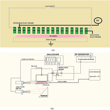
Figure 1. (a) Experimental setup of the perforated DBD source of plasma intensity and (b) vertical cross section of the perforated novel PCB source with power and ground connections.
Download figure:
Standard image High-resolution imageThis is different from our recently published paper with a similar source [32] where, apart from the configuration with the floating grid, we also analyzed configurations of the source with a powered grid and without the grid. Moreover, in that paper a 50 mm × 50 mm PCB plate served as grounded second electrode. Since the surface and the type of the second electrode are crucial for the I–V characteristics of the atmospheric DBD plasma reactor, changing these characteristics with respect to [32] will partially alter electrical properties of the source.
In figure 1(b) we show the source with schematics of electrical and detection parts of the setup. The perforated PCB is fixed at the bottom of a Plexiglas box with a hole for gas inlet at the top side. This way, uniform gas flow through all PCB holes is achieved. The powered electrode is connected through an L-type custom-made matching network to a 13.56 MHz power supply. In all experiments we had reflected power set to the minimal value and kept below 3% of the forwarded power. This was set before the measurements and we did not need to change the settings of the matching network afterwards during the measurements. Therefore, the L–C values of the matching network did not change. All this implies that the DBD system is well balanced and its design gives close to optimal values when it comes to matching it to the power supply. The gap between electrodes was set at 2 mm. Pure helium was used as buffer gas at flow rates from 1 to 7 standard liters per minute (slm).
For the electrical characterization of the source, derivative probes were used to obtain voltage and current waveforms at the powered electrode. The voltage probe was a capacitive T-shaped probe and the current probe was an inductive Π-shaped probe, both placed inside a stainless-steel box which was connected in-line between the plasma source and the matching network [23, 24]. The V–I waveforms were recorded for different helium flow rates and power values using a 3000-X series digital oscilloscope from Agilent Technologies and then fast Fourier transform (FFT) was performed to obtain the voltage and current RMS values along with the total impedance of the source and the power dissipation (Pd). Power dissipation, voltage and current values V, I and phase difference φ were calculated using the waveform analysis software of the derivative probes. Due to the probe position, calculated dissipated power is not influenced by power losses from the cable and from the passive components of matching network and therefore represents only the power delivered to the DBD source.
For plasma imaging, we used an Andor ICCD camera iStar DH734I equipped with photographic lens NIKKOR 50 mm f/1.4 AIS [34]. Since electrodes were in horizontal position, a mirror was situated under the lower transparent FTO electrode reflecting the plasma emission to the camera. In addition to the surface plasma imaging described above, side on capturing of the plasma intensity was performed. Thus, we obtained images spectrally integrated in the visible spectral range. As the exposure time was in the order of several hundred µs, obtained images were time integrated observation of discharge emission from many RF periods. The objective was transparent for the light above 375 nm.
For the OES, an Acton Research Corporation SpectraPro-500 spectrograph with a ICCD camera was used. Plasma emission was guided by a fiber, positioned in the middle of the electrode gap, to an entrance slit of the spectrograph. Thus, the fiber collected light coming from a wide angle making the observed emission integrated in space, over the whole acceptance angle. These measurements were also time-integrated since they were taken with 5 s exposure time while the spectrally resolved emission from the plasma was recorded in a wide interval of wavelengths from 300 nm up to 800 nm in steps of 10 nm. A VIS-NIR 1000 µm optical fiber with reduced emission below 360 nm and stable response above 380 nm was used.
Poly-methyl methacrylate (PMMA) films spin coated on silicon wafers, were used for plasma etching. Samples of size approximately 2 cm × 2 cm were placed on the FTO electrode, and etching was performed for 120 s. A mixture of He/Air was used as etching gas, varying He flow rates at 2, 4 and 6 slm, while keeping the power constant at 100 W using a 13.56 MHz RF generator. A Woolam M2000 Spectroscopic ellipsometer was used for the ex situ measurements of PMMA film thickness before and after the plasma etching in order to determine the etching rate. Our new results show the important role of He flow rate, and are consistent with our first observations [32] using a constant He flow rate, and a PCB based bottom electrode. The high etching rates of this source have been used to etch paper and subsequently render it superhydrophobic [35].
3. Results and discussion
3.1. Electrical measurements
Electrical properties of the DBD source were obtained for different power values and helium flow rates when plasma is present. For each condition, a set of I–V curves was recorded using derivative probes, followed by calculation of the dissipated power and the impedance in the circuit during the plasma-on period. A power range from plasma ignition up to 120 Watt was studied for He flows 1, 2, 4, 6 and 7 slm. Figures 2(a)–(d) show respectively the RMS voltage, current, impedance and impedance phase obtained versus the dissipated power. In figure 2(b), current–voltage characteristics obtained for different He flows are shown. In figures 2(e) and (f) we present changes in the voltage amplitude of the 1st and the 3rd harmonic as a function of dissipated power and different flows.

Figure 2. Electrical measurements of perforated DBD source: (a) voltage versus dissipated power and He flow, (b) current change versus dissipated power and He flow, (c) impedance behavior (source + plasma) with dissipated power and He flow change, (d) phase change with the variation of flow and power, (e) 1st harmonic (13.56 MHz) change with dissipated power and He flow and (f) 3rd harmonic (40.68 MHz) change with the variation of dissipated power and He flow.
Download figure:
Standard image High-resolution imageIn figure 2(a) we can clearly see the effect of He flow on the ignition voltage for the same input power. Higher He flow results in lower ignition voltages. We also observe an increase of voltage with an increase of the dissipated power. Similar behavior is observed in the case of voltage variation with current, as shown in figure 2(b). From these two graphs, the amount of He has a significant effect on the discharge working point. Namely, higher He flow rate results in an increase of He percentage in-between electrodes, lowering operating voltage of the plasma at a certain power. For the highest dissipated power of 110 W the difference in operating voltages between maximum and minimum flow rate is around 170 V. Additionally, current–voltage characteristic, shown in figure 2(b), indicate that current range also decreases with an increase of the flow rate. Therefore, at certain power forwarded to the source the discharge will operate at a lower current when the gas flow rate is higher.
As expected, from the voltage and current curves and assuming that the impedance of the source is constant, in figure 2(c) we see that the absolute values of the plasma impedance decreases both with increasing He flow rate and input power as a consequence of higher efficiency of the discharge due to the presence of He [36], indicating enhanced electron density in the plasma. In figure 2(d) we present the phase difference between the voltage and current signals (related to the imaginary component of the impedance) as a function of both He flow rate and input power. The negative sign of the phase difference indicates a capacitive behavior of the source that decreases slightly with an increasing input power. On the other hand, the increasing He flow rate has a more important effect on the impedance phase, leading to lower phase difference values, i.e. less capacitive behavior of the DBD source.
Plasmas are in general highly asymmetric systems and as a result this influences the appearance of a number of higher harmonics. The amplitudes of signals at higher harmonic frequencies, other than the main operating frequency, are indicators of the asymmetry of the system. Design of the source i.e. its construction will govern the number of harmonics that will appear. The number and intensity of harmonics are sensitive to impedance of the outer electrical circuit (matching box, cables and connectors) [37, 38]. In our case, for all He flow rates and all dissipated powers, FFT analysis showed an appearance of only the 3rd harmonic (40.68 MHz), which is two orders of magnitude smaller than the 1st harmonic (13.56 MHz). In figures 2(e) and (f) amplitudes extracted from the 1st and the 3rd harmonic after FFT analysis of the voltage signal are presented. The amplitude of the 1st harmonic increases with power. However, a decrease of the amplitude with an increase of the He flow is observed for all power levels. On the other hand, there is almost no change of the 3rd harmonic for all He flow rates and powers. This implies that asymmetry of our plasma system is not highly pronounced and that system itself is well balanced.
3.2. ICCD imaging
Recording of discharge images by ICCD camera was used to study plasma coverage of the electrode surface and it allowed us to establish optimal conditions for achieving uniform plasma operation over the entire electrode area. Measurements were performed for different He flow rates (1–7 slm) and for different dissipated power values. The end-on images obtained by using ICCD camera are presented in figures 3 and 4.
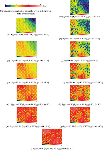
Figure 3. ICCD images of atmospheric pressure DBD operating with 7 slm of He for different RF input powers (PRF). Calculated dissipation powers (Pd) and measured RMS voltages are shown also. Images (a)–(f) taken with power increase and (g)(l) with power decrease. Chromatic presentation of intensity levels in images is in arbitrary units.
Download figure:
Standard image High-resolution image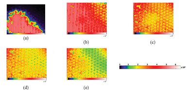
Figure 4. ICCD images of atmospheric pressure DBD for different helium flow rates at constant nominal power of the RF power 120 W. Dissipated power is indicated in parenthesis: (a) 1 slm He (109.8 W), (b) 2 slm He (108.3 W), (c) 4 slm He (110.1 W), (d) 6 slm He (111.9 W) and (e) 7 slm He (110.5 W). Chromatic presentation of intensity levels in (a)–(e) in arbitrary units.
Download figure:
Standard image High-resolution imageIn figures 3(a)–(f) we show images taken at 7 slm of helium flow, for powers starting from ignition of the plasma at 63.3 W up to the maximum dissipated power of 110.5 W. We can clearly see that the increase of power causes the plasma to spread over the whole electrode area. The emission intensity coming from the plasma also increases. In figures 3(f)–(l) we present images obtained when the dissipated power decreases having the same values as in figures 3(a)–(f). For example, the ICCD image in figure 3(g) was obtained for the same value of dissipated power as figure 3(e). The lowest dissipated power, where we could sustain plasma discharge was 51.8 W, and with further decrease of power plasma was turned off. This power value is lower than the one needed for the discharge ignition, demonstrating a hysteresis effect of the plasma and confirming that the ignition power is always higher than the power needed to sustain plasma. As the dissipated power decreases, at certain power values, the discharge coverage shown in figures 3(g)–(l) was slightly different (compared with the images figure 3(a)–(e)) with the emission intensity decreasing more rapidly with power. The appearance of the dark patches distributed almost randomly across the electrode surface could be observed as lower power was fed to the plasma. It appears that plasma is switching off at some local channels before other even neighboring channels. This all may be due to different conditions at the surface or slightly different distance of not perfectly parallel electrodes.
In figures 4(a)–(e) we show the effect of He flow rate on uniformity and emission intensity of the plasma. The experiments were performed at 120 W input power varying He flow rate from 1 up to 7 slm. As the discharge, current varies with the flow change, dissipated power is changing for different flows. We observe that full coverage of the electrode is obtained for He flow values of 2 slm and above (figures 4(b)–(e)). Moreover, as He flow rate increases the intensity of plasma emission drops. The main reason for this drop is the reduction of the percentage of air in the air/He mixture, which is further analyzed in section 3.3.
In figures 5(a)–(c) we present side-on images of the PCB based atmospheric pressure DBD device for three different flow rates. The experiments were performed at 120 W input power by using He flow rates of 2, 4 and 7 slm. We observed that when He flow rate increases the plasma intensity across the inter-electrode gap decreases. It is also clearly seen that there is a small convergence between the plates leading to a higher distance in the right side of the board. This may be due to lack of perfect flatness of the PCB boards, or not perfectly equal spacers separating the two PCB boards. Moreover, this differentiation of distance leads to a gradual increase of the plasma intensity and an increase on the plasma variance, as one moves from the left side to the right side. The increase in the emission intensity could be explained by the higher amount of surrounding air in the admixture.

Figure 5. ICCD images of atmospheric pressure DBD for different He flow rates at constant nominal power of the RF power 120 W. Dissipated power is indicated in parenthesis: (a) 2 slm He (108.3 W), (b) 4 slm He (110.1 W) and (c) 7 slm He (110.5 W). Chromatic presentation of intensity levels in (a)–(c) in arbitrary units.
Download figure:
Standard image High-resolution imageTo evaluate optimum conditions when full plasma coverage of the electrodes is achieved, a more comprehensive analysis was performed. A software code was developed for automatic image processing to find the mean intensity, intensity variation (error bar of the mean intensity) and the size of plasma covered area from the discharge images. This way we performed quantification of the plasma uniformity versus RF power as well as the effect of power on the mean plasma emission intensity.
In figure 6(a) we present the percentage of the DBD surface area covered by plasma as a function of nominal power forwarded from the power supply unit for He flow rate of 2, 4, 6 and 7 slm. The electrode part is considered as covered by plasma if the intensity level of that part of the image is above 92% of the maximum intensity in the image. Then, all such areas are summed and compared to the total electrode area. Herein we consider as electrode area only the area covered by holes (showerhead) which is equal to 80 × 80mm2 and not the entire electrode area (100 × 100 mm2) as the edge effects may affect significantly the measurements. We see in the figure that for all flows, as power increases, plasma spreads over the surface of the DBD and eventually covers the whole surface. The area covered by plasma between 92% and 100% is defined as full coverage. At higher He flow rates full coverage is reached at lower power levels. Namely, at 7 slm full coverage is reached from 75 Watts, while at 2 slm it is achieved at a power level above 110 Watts. Nevertheless, we observed that even with the lowest flow (2 slm) conditions, full plasma coverage can be achieved.
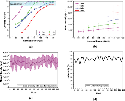
Figure 6. Results of quantitative analysis of ICCD images obtained for 2, 4, 6 and 7 slm of He. (a) Effect of power on plasma coverage of the DBD surface. (b) Effect of nominal power on the mean plasma intensity and its variation (c) column average emission intensity and its standard deviation along the X direction (i.e. from left to right), for figure 3(f). (d) Data of (c), plotted again as uniformity along the X direction.
Download figure:
Standard image High-resolution imageIn figure 6(b) we present the mean plasma emission intensity measured at 2, 4, 6 and 7 slm as a function of the nominal power for cases when the area covered by the plasma was larger than 92% i.e. with full coverage. The mean intensity values are calculated by dividing the sum of all pixel intensities by the pixel number (240 × 240 pixels). As expected, the mean intensity increases with power for all He flow rates. The intensity for 2 slm is the highest while for higher He flow rates the intensity drops.
To quantify in more detail the uniformity of the plasma on the PCB, we calculated the mean pixel intensity and its standard deviation for each column along the X direction for figure 3(f), corresponding to typical operating conditions of 7 slm He and 120 W. In figure 6(c) we show the plasma variation obtained from such averaged emission intensity data (from figure 3(f)) along the 240 columns in the X direction (i.e from left to right). In figure 6(d) we plot again these data to show the uniformity of the plasma along the X direction. The uniformity (in %) is calculated as (1 − ((|standard deviation|)/(mean Intensity))) * 100. The uniformity variation shown is due to the showerhead-type of the powered electrode. The holes on the PCB cause small local emission intensity variations, i.e. slightly lower plasma emission intensity in the position of the holes compared to the position in between the holes. Nonetheless, the level of plasma uniformity stays almost constant in a wide range of operating power, especially for higher He flow. This feature of the DBD source is very important for homogeneous treatments of large area samples.
3.3. Optical emission spectroscopy
In figure 7 we present emission spectra obtained at 100 Watt nominal power obtained for a wide range of wavelengths between 300 nm and 800 nm. The atomic O, the first negative system (FNS) of N2 ion as well as the second positive system (SPS) of N2 molecular transition lines are visible in the spectrum. For He there are no excitation thresholds below 19 eV, and therefore most of the excitation and ionization is due to oxygen and nitrogen. Even at 19 eV it is the metastable levels of He that would quickly transfer excitation to FNS lines of nitrogen and equivalent levels of oxygen. We also observe in figure 7 electron energy levels from He 707 line, i.e. from electrons with energy higher than 22 eV.

Figure 7. Optical emission spectroscopy of atmospheric pressure DBD at helium flow rate 5 slm and nominal power 100 W.
Download figure:
Standard image High-resolution imageThe results of optical emission spectrometry (OES) obtained for different power values and flow rates are presented in figure 8: we show the total emission intensity of the plasma recorded by the spectrometer in the range between 380 to 800 nm, the intensities of atomic O at 777 nm, He at 707 nm and the intensity of (0–2) SPS N2 molecular transition line (at 380 nm). We only present the 380 nm SPS N2 line due to our optical fiber limitations, which reduces the emission below 360 nm and has a stable response above 380 nm. The line intensities are corrected for the efficiency of the optical system using a curve obtained from the supplier, Princeton Instruments. However, correction due to the optical fiber limited response below 360 nm has not been applied.

Figure 8. Effect of He flow rate and power to the total emission intensity (380–800 nm), intensity of O 777 nm, He 707 nm and SPS 380 nm N2 band line. Atmospheric pressure DBD with (a) nominal power 100 W, (b) He flow rate 5 slm.
Download figure:
Standard image High-resolution image
In figure 8(a) left Y axis we can see the effect of He flow rate on the emission intensities when applying a constant 100 W input power. As expected, the He flow rate increase results in increase of the He 707 nm line intensity due to the higher percentage of He in the He-surrounding air gas mixture. The emission intensity can be calculated as a function of the gas density, excitation coefficient and electron density. The emission of Oxygen also increases, although we expect a slight drop of its density at high flowrates. The increased Oxygen emission is probably due to higher electron density and/or higher excitation coefficient (due to higher electron temperature); such increases may offset any decrease of Oxygen density [39]. If we assume that the excitation coefficient ratio of He at 707 nm and O at 777.2 nm remains almost constant with flowrate, we can estimate the effect He flow rate on O density, by taking the emission intensity ratio of O/He (see figure 8(a) right Y axis). We observe that the ratio of intensities decreases, and this is an indication of reduced oxygen atom density at higher flowrates. Similar effects have been observed in He–O2 mixtures [25, 40]. As we will see below this reduction of the Oxygen atom density is consistent with the reduction of the etching rate at high flowrates.
Contrary to He and Oxygen emissions, the N2 380 nm intensity drops almost one order of magnitude as He flow changes from 2 slm to 8 slm and smaller amount of air is present between electrodes. Such behavior of total emission and N2 380 line intensities suggests that dominant part of the spectrally integrated emission belongs to lines in N2 SPS band.
Figure 8(b) shows the effect of input power on intensities of the same lines using 5 slm He flow rate. As expected, the power increase results in higher peak intensities of the N2 380 nm line and He lines. Finally, in both figures 7(a) and (b) we see that the total emission intensity of the plasma follows the N2 380 nm line intensity. Therefore, we conclude that the dominant emission is the N2 SPS molecular transition lines, which define the total emission intensity of the plasma.
3.4. Etching and wetting properties of PMMA films
Treatment of polymeric substrates was also performed with the DBD plasma source. PMMA (Poly methyl methacrylate) thin polymeric films spin-coated on silicon were etched with the DBD source in He/air plasma. Film thickness measurements were performed using multiwavelength ellipsometry before and after plasma etching and the etch rates of polymer films were calculated. For the treatment with He/air we used 100 Watt as nominal power and He flows of 2, 4 and 6 slm. All the samples were etched for 2 min. In table 1 we can see the effect of the change of He flow rate on the etch rates, i.e. as He flow rate increases etching rate drops. This is consistent with decreased density of atomic oxygen at high flowrates, as observed by the emission intensity ratios shown above in figure 8(a) for Oxygen and Helium. At high flowrates it is also possible that the etching rate is reduced due to convective cooling of the sample from the He flow.
Table 1. PMMA etching rates and corresponding contact angle values after six weeks of ageing as a function of He flow rate at constant nominal power 100 W.
| Power (Watt) | He (slm) | Etch rate (nm min−1 ± 10) | Contact angle after 6 weeks (±3°) |
|---|---|---|---|
| 100 | 6 | 52 | 45 |
| 100 | 4 | 69 | 41 |
| 100 | 2 | 93 | 35 |
It has been shown before that plasma treatments may affect surface hydrophilicity [32]. Namely, PMMA films before treatments had contact angles approximately 70°. After the treatment surfaces became more hydrophilic, with a lower contact angle approximately 30°. We re-measured the static contact angles of the treated PMMA samples six weeks later between 40° to 50°. This result showed that aging of treated surfaces with He/air plasmas has not been significant and the surfaces remained hydrophilic, especially those treated with low He flow rates.
4. Conclusion
In this work, we present a comprehensive analysis of characteristics of the plasma generated by a novel PCB based atmospheric pressure DBD source. We performed electrical characterization, by using derivative probes, simultaneously with optical diagnostics: plasma imaging and OES. By using the data obtained from electrical measurements, we determined voltage–current characteristics and calculated power dissipation at the plasma source. We showed that behavior of the electrical properties of the DBD are strongly affected by the He-surrounding air mixture, i.e. related to the He flow. From the analysis of higher-order harmonics we demonstrated electrical stability of operation of the source. In addition, ICCD recordings of spatially-resolved images and optical spectra of the discharge provided information about plasma structure at different operating parameters. We systematically studied the effect of He flow rate and the power forwarded to the device on the uniformity and emission intensity of the plasma, attaining the parameter range of powers and flow rates with high plasma uniformity. The high plasma uniformity makes the discharge source suitable for material processing over potentially large areas.
We also performed polymer treatment with the DBD source in terms of PMMA etching and wetting measurements. We concluded that PMMA surface aging has been significantly retarded and the surfaces remained hydrophilic even after six weeks, especially those treated with low He flow.
The source that has been built allows non-equilibrium plasma formation over a wide area. It presents high uniformity, all the benefits of DBD operating in glow regime without filamentation, and it is well controlled by adjusting the gas flow, mixture composition and power. Other modes of operation are worth exploring such as using Ar as a buffer gas, allowing a more complex chemistry and allowing pulsing and two frequency operation.
Acknowledgments
This work was financed by the NATO project SPS 984555. The COST project MP1101 funded the short-term mission of Angelos Zeniou to IOP in Belgrade for the electrical and optical measurements. Authors from the Institute of Physics acknowledge projects of MESTD of Republic of Serbia ON171037 and III41011.