
Abstract
SiNx layers intended for photonic applications are typically fabricated using LPCVD and PECVD. These techniques rely on high-temperature processing (>400 °C) to obtain low propagation losses. An alternative version of PECVD SiNx layers deposited at temperatures below 400 °C with a recipe that does not use ammonia (NH3-free PECVD) was previously demonstrated to be a good option to fabricate strip waveguides with propagation losses <3 dB cm−1. We have conducted a systematic investigation of the influence of the deposition parameters on the material and optical properties of NH3-free PECVD SiNx layers fabricated at 350 °C using a design of experiments methodology. In particular, this paper discusses the effect of the SiH4 flow, RF power, chamber pressure and substrate on the structure, uniformity, roughness, deposition rate, refractive index, chemical composition, bond structure and H content of NH3-free PECVD SiNx layers. The results show that the properties and the propagation losses of the studied SiNx layers depend entirely on their compositional N/Si ratio, which is in fact the only parameter that can be directly tuned using the deposition parameters along with the film uniformity and deposition rate. These observations provide the means to optimise the propagation losses of the layers for photonic applications through the deposition parameters. In fact, we have been able to fabricate SiNx waveguides with H content <20%, good uniformity and propagation losses of 1.5 dB cm−1 at 1550 nm and <1 dB cm−1 at 1310 nm. As a result, this study can potentially help optimise the properties of the studied SiNx layers for different applications.
Export citation and abstract BibTeX RIS

Original content from this work may be used under the terms of the Creative Commons Attribution 3.0 licence. Any further distribution of this work must maintain attribution to the author(s) and the title of the work, journal citation and DOI.
1. Introduction
Silicon nitride (SiNx) is a CMOS-compatible material that has a wide transparency window that makes it viable for applications covering the ultra-violet to the mid-infrared (250 nm–7 μm) [1, 2]. It also has the advantage of exhibiting low non-linear losses, which are useful for non-linear applications [3]. In recent years, it has drawn attention as a potential alternative for a variety of photonic devices mostly because its physical, chemical and optical properties can be tailored through the deposition conditions to fulfil the requirements of different applications [4, 5]. Amongst these applications, SiNx films have proved particularly attractive for passive waveguides due to the refractive index of the material (1.7–2.8) capable of providing tight optical confinement with low propagation losses over a wide wavelength range [6–8].
SiNx layers are typically fabricated using low pressure chemical vapour deposition (LPCVD) [9, 10] and plasma enhanced chemical vapour deposition (PECVD) [11, 12]. LPCVD layers processed at high temperatures (>800 °C) show losses below 1 dB cm−1 [6, 12], while PECVD layers processed at relatively lower temperatures (<400 °C) exhibit losses >3 dB cm−1 unless they are annealed at temperatures above 600 °C [12–14]. In both cases, high temperatures are needed to provide the kinetic energy required to eliminate the hydrogen impurities incorporated into the films. This is important because the hydrogen impurities, in the form of N-H and Si-H bonds, act as absorption centres responsible for the propagation losses at telecomm wavelengths [11, 15–17]. However, processing temperatures above 400 °C are incompatible with the back-end-of-line (BEOL) integration needed to fabricate photonic devices in multilayer platforms.
The hydrogen impurities incorporated in the standard PECVD SiNx films come mostly from the density of hydrogen present in the deposition precursor gases, silane (SiH4) and ammonia (NH3) [11]. An alternative way to reduce these impurities without using high temperatures is to replace NH3 with N2 to reduce the amount of hydrogen available during deposition. This modified version of the standard PECVD recipe for SiNx (NH3-free PECVD) has previously demonstrated to be a good alternative for the fabrication of layers with low hydrogen content at low processing temperatures that have the potential to provide propagation losses <3 dB cm−1 [11, 18]. Nevertheless, little is understood of how the deposition conditions affect the material and optical properties of the layers and how these properties affect the performance of the SiNx devices intended for photonic applications.
In this work, we conducted a systematic investigation of the effect of the deposition parameters on the material and optical properties of NH3-free PECVD SiNx layers using a design of experiments methodology (DoE) [19]. We focused mostly on understanding how the deposition conditions affect the properties that have a significant impact on the fabrication and performance of photonic devices. We deposited PECVD SiNx films at 350 °C using different combinations of SiH4 flow, RF power, chamber pressure and substrates. Then, we characterised the films with ellipsometry to measure their refractive index and uniformity, scanning electron microscopy (SEM) to evaluate their material structure, atomic force microscopy (AFM) to scan their roughness [20, 21], and Fourier transform infrared spectroscopy (FTIR) to determine their chemical structure, bond structure and hydrogen content (H%) [16, 22]. Finally, we fabricated waveguide structures with different lengths to study the propagation losses of the SiNx films at 1310 and 1550 nm using the cut-back method, so that the propagation losses of the deposited films can be optimised later for waveguide applications. Other deposition parameters, such as substrate temperature, might also have a significant effect on the optical properties of the films, however they were out of the scope of this work as we targeted a maximum deposition temperature of 350 °C.
2. Methods
2.1. Methodology
The aim of this study was to optimise the deposition recipe of SiNx films prepared by NH3-free PECVD in order to obtain the best properties and the lowest propagation losses possible for photonic applications. The study was carried out using the Oxford Plasma Technology 100 PECVD system, employing the deposition recipe suggested by the manufacturer as a starting point with a SiH4:N2 chemistry (1.8:1000 sccm), a radio frequency generator (RF) power of 60 W, and chamber pressure of 650 mTorr.
We generated different central composite designs (CCD) with Minitab to study the effect of the SiH4 flow and the RF power on the material and optical properties of the films following a similar approach to the one described by Tien et al [19], in order to have enough information to estimate how the properties of the layers would change if these deposition parameters were altered in any direction. Once we had a general overview, we focused on 9 experiments that included the factors and levels detailed in section (a) of table 1. The relations estimated from these experiments were confirmed afterwards by conducting tests that included additional factor combinations within the experimental region.
Table 1. Deposition parameters, control factors and factor levels defined for each set of DoE experiments.
| (a) Set 1: Effect of SiH4 flow and RF power | |||||
|---|---|---|---|---|---|
| Fixed parameters | |||||
| N2 flow (sccm) | 980 | ||||
| Pressure (mTorr) | 650 | ||||
| Control factors | Factor levels | ||||
| SiH4 flow (sccm) | 1.5 | 2.0 | 3.0 | ||
| RF power (W) | 20 | 60 | 100 | ||
| (b) Set 2: Effect of N2 flow and SiH4 flow | |||||
|---|---|---|---|---|---|
| Fixed parameters | |||||
| RF power (W) | 60 | ||||
| Pressure (mTorr) | 950 | ||||
| Control factors | Factor levels | ||||
| N2 flow (sccm) | 650 | 750 | 850 | 980 | |
| SiH4 flow (sccm) | 1.5 | 3.6 | |||
| (c) Set 3: Effect of chamber pressure | |||||
|---|---|---|---|---|---|
| Fixed parameters | |||||
| SiH4 flow (sccm) | 1.5 | ||||
| N2 flow (sccm) | 980 | ||||
| RF power (W) | 60 | ||||
| Control factors | Factor levels | ||||
| Pressure (mTorr) | 650 | 750 | 850 | 950 | 1000 |
Similarly, we considered the effect of the N2 flow on the structural properties of the SiNx layers and its interaction with the SiH4 flow using a experimental design that included 8 experiments with the factor variations defined in section (b) of table 1.
We also studied the effect of the chamber pressure on the properties of the SiNx films by varying this parameter from 650 to 1000 mTorr using the deposition conditions described in section (c) of table 1.
Finally, we deposited SiNx films on substrates with SiO2 layers that were grown either by PECVD or thermal oxidation in order to study the effect of the SiO2 layers on the propagation losses of SiNx strip waveguides.
2.2. Fabrication
All the films were deposited at a substrate temperature of 350 °C using the recipes defined in the previous section. The recipes were deposited on bare Si samples ( cm) targeting thicknesses close to 300 nm for deposition rate, ellipsometry, SEM, AFM and FTIR characterisation. Once the deposition rates were known, films with a thickness of 300 nm were deposited on samples with SiO2/Si stacks (
 cm) to fabricate strip waveguides for propagation loss measurements. The SiO2/Si stacks had a layer of either PECVD SiO2 or thermal SiO2 with a thickness greater than 2 μm to minimise the losses produced by the leakage of optical modes to the Si substrate.
The layout fabricated on the SiO2/Si stacks included two sets of waveguides with lengths up to 1.7 cm to measure the optical losses of the SiNx layers at 1310 and 1550 nm. The width of the strip waveguides was optimised to provide single-mode propagation for both TE and TM polarisations. The waveguides intended for measurements at 1310 nm had a width of 900 nm, while the waveguides for 1550 nm had a width of 1200 nm. In both cases, the designs included grating couplers optimised to have high coupling efficiency (CE) for TE polarisation at each targeted wavelength. The grating couplers for 1310 nm had a theoretical CE ∼ 58% with a period of 1 μm and filling factor of 50%, while the ones for 1550 nm had a theoretical CE ∼ 40% with a period of 1.2 μm and 50% filling factor.
Both waveguides and grating coupler were patterned on the SiO2/Si stack samples using electron beam lithography with a 450 nm thick resist (ZEP520A) and conventional inductive coupled plasma (ICP) etch using a SF6:CHF3 chemistry. The waveguides were finally covered with a 530 nm PECVD SiO2 layer deposited at 350 °C as a top cladding.
2.3. Characterisation
The material and optical properties of the SiNx layers were systematically evaluated using different characterisation techniques. High-resolution scanning electron microscopy (SEM) was used to take cross-sectional images of each deposited layer in order to estimate their thickness, deposition rate and material structure. Atomic force microscopy (AFM) was used to characterise quantitatively the surface roughness of the layers by measuring their root-mean-square roughness (RMS) on a  μm area. Ellipsometry carried out with an M2000DI ellipsometer was used to determine the thickness uniformity and refractive index of the layers at 632.8 nm. This refractive index (n) was used to estimate the N/Si ratio using equation (1) as proposed by Bustarret et al [16] and Mackel et al [23] using
  for silicon and
  for stoichiometric Si3N4.
FTIR spectroscopy was carried out using a Varian 600 FTIR spectrometer to determine the compositional structure of the layers including their bond concentration, atom concentration and hydrogen content. The different bond concentrations were obtained from the FTIR spectra after baseline correction with the method described by Yin and Smith [17] using the proportionality factors  cm−1 and
  cm−1 proposed by Lanford and Rand [15], and the proportionality factor
  cm−1 given by Bustarret et al [16]. The hydrogen and nitrogen atom concentrations (
![$\left[\text{H}\right]$](https://content.cld.iop.org/journals/0022-3727/50/2/025106/revision1/daa4b91ieqn009.gif) and
and ![$\left[\text{N}\right]$](https://content.cld.iop.org/journals/0022-3727/50/2/025106/revision1/daa4b91ieqn010.gif) ) were then estimated using expressions (2) and (3) [16, 17].
) were then estimated using expressions (2) and (3) [16, 17].


Where ![$\left[\text{N}-\text{H}\right]$](https://content.cld.iop.org/journals/0022-3727/50/2/025106/revision1/daa4b91ieqn011.gif) ,
, ![$\left[\text{Si}-\text{H}\right]$](https://content.cld.iop.org/journals/0022-3727/50/2/025106/revision1/daa4b91ieqn012.gif) and
and ![$\left[\text{Si}-\text{N}\right]$](https://content.cld.iop.org/journals/0022-3727/50/2/025106/revision1/daa4b91ieqn013.gif) are the concentrations of N-H, Si-H and Si-N bonds, respectively.
are the concentrations of N-H, Si-H and Si-N bonds, respectively.
The Si atom and Si–Si bond concentrations (![$\left[\text{Si}\right]$](https://content.cld.iop.org/journals/0022-3727/50/2/025106/revision1/daa4b91ieqn014.gif) and
and ![$\left[\text{Si--Si}\right]$](https://content.cld.iop.org/journals/0022-3727/50/2/025106/revision1/daa4b91ieqn015.gif) ) were calculated separately using the N/Si ratio (x) previously estimated from the refractive index using equations (4) and (5) proposed by Mäckel and Lüdemann [23].
) were calculated separately using the N/Si ratio (x) previously estimated from the refractive index using equations (4) and (5) proposed by Mäckel and Lüdemann [23].


Finally, the cutback method was used to measure the propagation losses of each layer using the Agilent 8163B and 8164B Lightwave systems to obtain the spectral response of the fabricated waveguides at 1550 and 1310 nm respectively.
3. Results and discussion
3.1. Material structure
The structure of the deposited films is important for propagation losses because grains, pores, defects and rough interfaces are a direct cause of scattering losses [24]. Figure 1 contains SEM images that show the microstructure of some of the deposited SiNx films and their interface with the Si substrate. Image (a) shows a SiNx layer with excess nitrogen (N-rich), image (b) a layer close to stoichiometry (Si3N4) and image (c) a layer with excess silicon (Si-rich). All the films adhere well to the substrate, are free of cracks and have an amorphous structure with no significant changes along the growth direction.

Figure 1. SEM cross-sections of: (a) N-rich SiNx films with a porous micro-columnar structure and (b) SiNx films close to stoichiometry with a more homogeneous structure and (c) Si-rich SiNx film with a porous structure.
Download figure:
Standard image High-resolution imageThe N-rich and Si-rich samples are porous and have a microstructure with columnar growth that resembles the classic appearance of the Zone I type films detailed by Kaiser [24]. This structure can be attributed to the statistical roughening and self-shadowing processes that occur due to the low surface mobility and high sticking coefficient of the species when the surface temperature is low compared to the melting temperature of the deposited materials [24, 25].
These observations are in line with a previous study in which Smith demonstrated that standard PECVD SiNx layers appear to be completely homogeneous compared to NH3-free PECVD layers [25]. However, we have proved that the lower density regions between the columns tend to disappear when the chemical composition of the samples moves towards stoichiometry leading to more homogeneous, smooth and dense films as seen in figure 1. This improved microstructure is desirable to achieve light propagation with low losses.
3.2. Deposition rate
The majority of the physical and optical properties of the SiNx layers are highly dependent on their thickness and morphology. Examining the behaviour of their deposition rates is important because it affects the nucleation processes that determine the morphology of the deposited layers and it also allows a greater control over the film thickness. Our study suggests that all of the parameters: SiH4 flow, N2 flow, RF power and chamber pressure, affect directly the deposition rate of the NH3-free SiNx layers without interaction between them as illustrated in figure 2. In this case, the deposition rate increases when either the SiH4 flow, RF power or chamber pressure are increased during deposition, while it decreases when the N2 flow rises. Still, the deposition rate is more strongly affected by the RF power, which means that the deposition reaction is mostly plasma power limited.
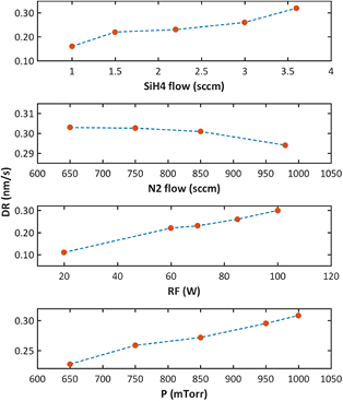
Figure 2. Deposition rate as a function of the deposition parameters. The deposition rate increases with increasing SiH4 flow, RF power and pressure, while it decreases with increasing N2 flow. The constant parameters considered for each case are (a) N2 = 980 sccm, RF = 60 W and  mTorr, (b) SiH4 = 1.5 sccm, RF = 60 W, and
  mTorr, (c) SiH4 = 1.5 sccm, N2 = 980 sccm and
  mTorr, (d) SiH4 = 1.5 sccm, N2 = 980 sccm and RF = 60 W. The dashed lines are a guide to the eye.
Download figure:
Standard image High-resolution imageThe deposition rate increases by 30% when the SiH4 flow is doubled. A similar trend in the deposition rate of NH3-free PECVD films with varying SiH4 flow has been observed in the literature and can be explained by the higher proportion of Si radicals available that are incorporated into the films in the form of high density Si atoms when the SiH4 fraction is higher [11, 18]. We believe that the deposition conditions allow the complete dissociation of the SiH4 and that the process is limited by the N2 concentration in such a way that an increased number of Si species can be incorporated if there are still N species that can be consumed. Hence, this tendency is only observed because the amount of available Si species is smaller than the amount of N species. Otherwise, it would be expected to see a saturation of the deposition rate at a maximum value due to the depletion of N reactants as Karouta observed in PECVD SiNx films deposited with higher SiH4 fractions [18].
On the contrary, the deposition rate decreases slightly when the N2 flow is increased by 1.5 times. This effect is expected, since it is equivalent to reducing the SiH4 flow and can be explained by the reduction of the proportion of Si species available for deposition. This effect is similar to the one observed by other authors with standard PECVD layers when increasing the NH3 or N2 flow [26]. In fact, it can also be observed in the results presented by Mao for NH3-free layers [11], but the decrease in deposition rate in that case is stronger. We believe that this difference in the strength of the effect is due to the fact that there was an excess of N species in all the recipes that were tested in this study.
The deposition rate doubles for a 5 times increase in RF power. There is no precedent on the obtained trend between the deposition rate and RF power in NH3-free films. Nevertheless, the behaviour is similar to the one described by several authors in both PECVD SiNx and SiON films [18, 26, 27]. The deposition rate increases because the higher RF power provides higher plasma energy that results in larger concentrations of active species that raise the incorporation of Si and N atoms into the films making them become thicker in shorter time. This last result is contrary to the trend observed by Mao in NH3-free films [11], but the discrepancy can be explained by the use of a different reactor and RF powers that are at least one order of magnitude higher than the ones used in this study.
Finally, the deposition rate increases by about 30% when the pressure is increased 1.5 times. As with the RF power, there is no precedent in this result but is similar to the effect observed in PECVD SiNx [26] and PECVD SiON layers [27]. The higher deposition rates achieved with higher pressures are related to the increase in residence time that occurs on the precursor gases with increasing total pressure. For instance, the high dissociation efficiency of SiH4 leads to the creation of more Si radicals when the residence time is longer, achieving an effect similar to the one obtained with higher RF powers that increases the deposition rate.
In general, high deposition rates are desirable to speed up the fabrication process and reduce the cost of photonic industrial applications. In this case, we achieved deposition rates as high as 20 nm min−1. This deposition rate is about one order of magnitude higher than the typical rate for LPCVD SiNx films, but still not higher than the rates observed in standard PECVD SiNx films. As a result, NH3-free PECVD SiNx layers can not be considered as an alternative for improving the deposition time during fabrication. They can only be seen as an alternative for obtaining lower propagation losses without reducing the deposition rate that is already being used with standard PECVD layers.
3.3. Thickness uniformity
Thickness uniformity is important in order to achieve consistent dimensions over large substrate areas when fabricating photonic devices for commercial applications. In this study we quantified the thickness uniformity of NH3-free PECVD SiNx layers deposited on 6'' wafers in terms of their non-uniformity percentage, which is defined by expression (6) [28]:

where tmax is the maximum thickness, tmin the minimum thickness and tmean the mean thickness measured in a 6'' wafer.
The experiments show that the non-uniformity percentage of the NH3-free PECVD SiNx layers has only a clear relationship with the RF power and pressure used during deposition. Figure 3 indicates that the non-uniformity percentage increases with increasing RF power at the same time that it decreases with increasing pressure. This result is consistent with the observation of other authors when depositing SiNx with the standard PECVD recipe [29, 30].

Figure 3. Thickness non-uniformity as a function of deposition parameters. The non-uniformity increases with increasing RF power and decreases with increasing pressure. The constant parameters considered for each case are (a) SiH4 = 1.5 sccm, N2 = 980 sccm and  mTorr, (b) SiH4 = 1.5 sccm, N2 = 980 sccm and RF = 60 W. The dashed lines are a guide to the eye.
Download figure:
Standard image High-resolution imageThe large thickness non-uniformity observed at higher RF powers is mainly due to the high growth rates achieved under these conditions, as they cause a depletion of precursors that allows intermediate active species to stream over the substrate. This effect can be boosted by the lower stability that the plasma has when the RF power is high as pointed out by Wei et al [30]. Nevertheless, the thickness non-uniformity of the layers can be reduced by increasing the pressure regardless of the RF power because there is a better gas distribution uniformity during deposition at high pressures. We observed that the non-uniformity drastically reduces when the pressure is increased to 950 mTorr and therefore we opted to use this value for our fabrication process. In fact, we were able to reduce the overall wafer non-uniformity of the layers deposited at 650 mTorr from 15% to values as low as 3% for nearly stoichiometric layers and 1% for Si-rich layers as illustrated in figure 4.
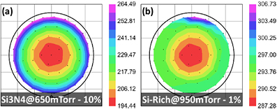
Figure 4. Overall non-uniformity of SiNx layers deposited on 6'' wafers at (a)  mTorr and (b)
  mTorr. The non-uniformity can be reduced from 10% to <2% when the pressure is increased from 650 to 950 mTorr.
Download figure:
Standard image High-resolution imageIn most cases, the thickness non-uniformity of the NH3-free PECVD layers is slightly higher than that of standard PECVD SiNx films which is typically <2.5% [29]. Yet, we have demonstrated that NH3-free PECVD layers with relatively low non-uniformity can be achieved when the chamber pressure is high. For similar deposition parameters, the non-uniformity of the NH3-free PECVD layers is comparable to that of standard PECVD films.
3.4. N/Si ratio
Our study suggests that, even though the rest of the optical and structural properties of the NH3-free SiNx layers seem altered by the deposition conditions, the observed changes only reflect the effect that the deposition parameters have on the N/Si ratio of the films. In fact, our experiments revealed that the only structural parameter that can be modified directly with the deposition conditions is the N/Si ratio of the films. This dependence is important because it gives the ability of tuning the characteristics of the SiNx layers for specific applications. It is just a matter of using the deposition parameters to change the composition of the layers to obtain either N-rich, Si-rich or stoichiometric layers.
The experiments conducted in this study show that the N/Si ratio can be tuned between 0.6 and 1.7 by modifying either the SiH4 flow, N2 flow, RF power or chamber pressure used for deposition as illustrated in figure 5. In this case, the N/Si ratio decreases when either the SiH4 flow or the pressure are increased, while it increases when the N2 flow or the RF power are augmented. In all cases, it can be observed that the depletion of reactants causes a saturation trend in the N/Si ratio of the films. Nevertheless, the RF power is the parameter that has the strongest effect on the N/Si ratio of the films.

Figure 5. N/Si ratio as a function of the deposition parameters. The N/Si ratio decreases with increasing SiH4 flow and pressure, while it increases with increasing N2 flow and RF power. The constant parameters considered for each case are (a) N2 = 980 sccm, RF = 60 W and  mTorr, (b) SiH4 = 1.5 sccm, RF = 60 W, and
  mTorr, (c) SiH4 = 1.5 sccm, N2 = 980 sccm and
  mTorr, (d) SiH4 = 1.5 sccm, N2 = 980 sccm and RF = 60 W. The dashed lines are a guide to the eyes.
Download figure:
Standard image High-resolution imageThe N/Si ratio decreases by 30% when the SiH4 flow is doubled. This tendency was previously observed by other authors [18, 31] and indicates a higher incorporation of Si into the films due to the increased availability of Si species when the SiH4 flow is high. On the contrary, the N/Si ratio slightly increases when the N2 flow increases due to the reduction of the Si species available for deposition. This effect is equivalent to a reduction of the SiH4 flow similar to the one observed in the deposition rates of the films.
The N/Si ratio doubles when the RF is increased by 5 times. This behaviour can be associated to the higher energies needed to dissociate N2 molecules compared to SiH4 molecules. N-rich materials are produced at high RF powers because there is enough energy available to increase the concentration of N radicals that are incorporated in the form of N bonds. This result is in line with the observations of Karouta when depositing PECVD SiNx layers [18], but it is contrary to the behaviour described by Han et al [31]. However, Han's observations can be explained by their use of a different reactor and considerably higher RF powers that result in a fundamentally different experiment. In general, the results suggest that a RF power around 60 W is appropriate to obtain N/Si ratios that can be tuned by changing the SiH4 and N2 flow rates, as the N/Si ratio tends to saturate when the RF power is higher.
Finally, the N/Si ratio decreases slightly when the chamber pressure is increased. This behaviour is related to the increased residence time of the precursor gases at high pressures, because more SiH4 is dissociated and incorporated in the films resulting in Si-rich compositions. This result is similar to what was observed by Lee et al on SiNx films deposited by ICP-CVD [32].
3.5. Refractive index
The refractive index of the SiNx layers is an important parameter for integrated photonic applications because it affects how the light is confined and propagated in the material. The experiments performed in the study show that the refractive index of the NH3-free SiNx layers is strongly related to their N/Si ratio regardless of the deposition parameters. For instance, the refractive index of the films can be tuned between 1.8 and 2.6 by changing their N/Si ratio from 0.6 to 1.7 as illustrated in figure 6. SiNx layers with N/Si > 1.33 have a N-rich structure that yields a lower refractive index useful for sensing, while SiNx layers with N/Si < 1.33 have a Si-rich composition that results in a relatively higher refractive index ideal for applications that require a higher confinement or higher non-linearity.
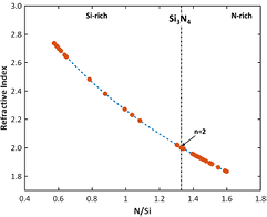
Figure 6. Refractive index of the NH3-free SiNx films measured at 632 nm as a function of N/Si ratio. The dashed line is a second-order polynomial trend. The refractive index decreases proportionally with the increasing N/Si ratio of the films and it has a value of 2 at the stoichiometric ratio of 1.33 indicated by the vertical line.
Download figure:
Standard image High-resolution image3.6. Bond structure
A typical SiNx FTIR spectrum, as the one shown in figure 7, reveals the presence of four major absorption peaks that can be used to extract the bonding configuration of a SiNx film. The peak around 450 cm−1 corresponds to the absorption of Si–Si bonds, the peak at 860 cm−1 to Si-N bonds, and, finally, the peaks at 2100 and 3300 cm−1 represent the absorption of Si-H and N-H bonds respectively [18, 33]. Both Si–Si and N-H covalent bonds are relevant to understand the propagation losses of SiNx films. Si–Si bonds are important defects in the SiNx matrix that lead to poor optical properties [17], while N-H bonds act as absorption centres that lead to undesirable losses in the 1510–1650 nm region [11]. As a result, the effect of both structural faults and their combination can produce high propagation losses in SiNx films.

Figure 7. FTIR spectra of a standard PECVD and a NH3-free PECVD SiNx layers showing the Si-N peak at ∼860 cm−1, the Si-H peak at ∼2200 cm−1, and the N-H peak at ∼3300 cm−1. The inset zooms in the Si-H and N-H peaks. The NH3-free PECVD SiNx layer has 8% lower hydrogen concentration compared to the one of the standard PECVD layer.
Download figure:
Standard image High-resolution imageThe experiments show that the different bond configurations of the NH3-free SiNx layers have a more intrinsic relation with the N/Si ratio than with the deposition conditions. Hence, the following results are expressed in terms of the N/Si ratio which can explain the observed behaviours in a more significant way than the deposition parameters.
Figure 8 shows the Si–Si and Si-N bond concentrations for different N/Si composition ratios. The concentration of the Si–Si bonds decreases with increasing N/Si ratios, which means they are dominant in Si-rich films and practically non-existent in N-rich films. This happens because the number of back-bonded Si atoms decreases in favour of N bonds that can be either present in the form of Si-N or N-H. These results are consistent with what has been reported in the literature for standard PECVD films [23, 34]. In contrast, the concentration of the Si-N bonds increases with the N/Si ratio until it reaches its maximum near N/Si  1.33 and then decreases when the N/Si ratio is increased further. The maximum value coincides with the stoichiometric value for the N/Si ratio which is where the Si and N atoms are balanced out.

Figure 8. Si–Si and Si-N bond concentration as a function of the N/Si ratio. The vertical line indicates the stoichiometric ratio of 1.33. The Si–Si bonds decrease with increasing N/Si ratio, while the Si-N bonds reach a maximum near the stoichiometric N/Si ratio. The dashed lines are a guide to the eyes.
Download figure:
Standard image High-resolution imageFigure 9 shows the Si-H and N-H bond concentrations as a function of the N/Si ratio of the deposited films. In this case, the Si-H concentration decreases with increasing N/Si ratio,while the N-H concentration increases. This happens due to the competing nature of the formation of both types of bonds [34] and the availability of more Si or N radicals with the different N/Si ratios. In consequence, Si-rich films tend to have more Si-H bonds and N-rich films more N-H bonds.

Figure 9. Si-H and N-H bond concentrations for different N/Si ratios. The vertical line indicates the stoichiometric ratio of 1.33. Si-H bonds are dominant in Si-rich layers (N/Si < 1.33) and N-H bonds in N-rich layers (N/Si > 1.33). Both Si-H and N-H bond concentrations are almost the same near stoichiometry. The dashed lines are a guide to the eyes.
Download figure:
Standard image High-resolution image3.7. H concentration
The relative H concentration in atomic % (H%) can be determined from the bond concentrations calculated from the FTIR spectrum. This value is of the uttermost importance because it has been demonstrated that films with lower H concentrations tend to have lower propagation losses [11]. The results in figure 10 suggest that the H% decreases with increasing N/Si ratio until it reaches its minimum value near N/Si  1.33 and then increases back again. As a result, both Si-rich and N-rich films have a higher H% than stoichiometric films, which have the minimum H concentration and the maximum Si-N incorporation as demonstrated previously. Moreover, the results indicate that the lowest H% concentration obtained with the NH3-free recipe is 14.8%. This value is almost 10% lower than the H% typically observed in SiNx films deposited with the standard recipe [18]. This reduction in H% can only be attributed to the decreased Si-H and N-H absorbance peaks obtained with the NH3-free recipe as illustrated in figure 7. Hence, it is expected to achieve lower propagation losses with the NH3-free approach.

Figure 10. H% as a function of different N/Si ratio. The vertical line indicates the stoichiometric N/Si ratio of 1.33. The minimum value of 14.8% is obtained with nearly stoichiometric films. The H% of N-rich films is higher than that of Si-rich layers.
Download figure:
Standard image High-resolution image3.8. Roughness
The roughness is another important material parameter because it is one of the main sources of scattering losses that impact negatively the propagation losses of the deposited layers [21]. Figure 11 shows the RMS roughness measurements obtained from PECVD SiNx layers deposited on Si substrates using the standard and the NH3-free recipe with RF = 60 W and  mTorr. The RMS roughness of NH3-free layers ranges between 1.5 and 2.5 nm whereas that of standard PECVD layers tends to be below 1.5 nm. In general, the study suggests that the RMS roughness of the NH3-free films tends to be higher compared to that of the standard SiNx layers.
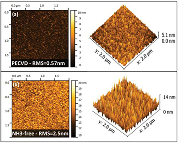
Figure 11. AFM micrographs with the RMS roughness of SiNx layers over  μm areas. Both layers are close to stoichiometry and were deposited using (a) the standard recipe and (b) the NH3-free recipe using RF = 60 and
  mTorr. The roughness of NH3-free layers is higher than that of standard PECVD layers.
Download figure:
Standard image High-resolution image3.9. Propagation losses
Materials with low propagation losses are needed to improve the performance of passive devices in integrated photonic circuits. As a result, it is desirable to understand how the deposition parameters and the structure of the deposited films influence the propagation losses of the NH3-free SiNx layers. The results obtained in this study suggest that no direct relation can be established between the varied deposition parameters and the measured propagation losses. However, in all cases the losses at 1310 and 1550 nm are intrinsically correlated with the N/Si ratio of the films as illustrated in figure 12. This means that the propagation losses of the deposited layers are primarily a consequence of the structural properties of the films.

Figure 12. Propagation losses for NH3-free films with different N/Si ratios. The vertical line indicates the stoichiometric N/Si ratio of 1.33. Si-rich films have higher propagation losses at 1310 nm, while N-rich films at 1550 nm. The lowest propagation losses of 2 dB cm−1@1310 nm and 5 dB cm−1@1550 nm are obtained with N-rich and nearly stoichiometric films, respectively. The dashed lines are a guide to the eyes.
Download figure:
Standard image High-resolution imageThe propagation losses at 1310 nm decrease with increasing N/Si ratio in such a way that N-rich films have lower propagation losses at this wavelength. On the other hand, the propagation losses at 1550 nm follow a trend similar to that of the H concentration of the films. They decrease with increasing N/Si ratio until they reach a minimum value and then increase back again as the films become more N-rich. We believe that these behaviours suggest that the propagation losses at 1310 nm are the product of the Rayleigh scattering inherent to the microstructure of the deposited materials, whereas the propagation losses at 1550 nm are mostly the product of the absorption losses produced by the N-H bonds incorporated into the films. In this case, the propagation losses of Si-rich films are higher at 1310 nm because they have a microstructure with more defects due to the incorporation of both Si-H and Si–Si dangling bonds, while their losses at 1550 nm are lower because of the absence of N-H bonds in their structure. Alternatively, the propagation losses of N-rich films are higher at 1550 nm because of the presence of N-rich bonds in their structure that act as absorption centres at that particular wavelength. As a result, the lowest propagation losses are obtained simultaneously at both wavelengths with films that have a N/Si ratio close to stoichiometry because at this point the presence of H bonds is minimised and the microstructure defects produced by the Si dangling bonds are low.
The lowest propagation losses obtained are of 2 dB cm−1@1310 nm with N-rich layers and 5 dB cm−1@1550 nm with nearly stoichiometric films. Under this circumstances, the propagation losses at 1550 nm are still high compared to the losses of almost 4 dB cm−1@1550 nm measured on PECVD SiNx layers by Huang et al [12], even though the H content of NH3-free PECVD layers is almost 10% lower. This result suggests that the propagation losses of the NH3-free SiNx layers are not only affected by the microstructure and the H bonds of the material, but also by other external factors.
One of the factors that can potentially increase the propagation losses of the SiNx strip waveguides is the roughness of the SiO2 used to isolate them from the Si substrate. In fact, any surface roughness at the bottom or top of the films can lead to scattering that will increase considerably the propagation losses of the deposited materials. The PECVD SiO2 layers used in the previous experiments had a RMS roughness of almost 4 nm which is considerably higher than the RMS roughness of the Si substrate (0.2 nm) that was used on the roughness experiments. To rule out the effect of the SiO2 roughness, we changed the underlying layers for thermal SiO2 with a roughness below 2 nm. Figure 13 shows the propagation losses obtained for NH3-free PECVD SiNx layers with different N/Si ratios grown on the commercial SiO2. In this case, the propagation losses at both wavelengths have a behaviour respect to their N/Si ratio similar to the one observed in the films grown on the PECVD SiO2. However, the propagation losses at both wavelengths are reduced to values below 2 dB cm−1. In fact, we achieved propagation losses around 1.5 dB cm−1@1550 nm and below 1 dB cm−1@1310 nm with NH3-free PECVD SiNx layers just by improving the roughness and quality of the underlying SiO2.
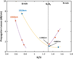
Figure 13. Propagation losses for NH3-free films with different N/Si ratios deposited on thermal SiO2. The vertical line indicates the stoichiometric N/Si ratio of 1.33. The lowest propagation losses obtained are of <1 dB cm−1@1310 nm for N-rich layers and 1.5 dB cm−1@1550 nm with nearly stoichiometric films. The dashed lines are a guide to the eyes.
Download figure:
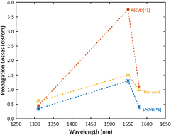
Standard image High-resolution imageFigure 14 shows the propagation losses obtained in this study compared to losses observed in the literature. The propagation losses of the NH3-free films are lower than those obtained with similar PECVD layers that have not been subjected to high temperatures. In this case, the propagation losses at 1310 nm are almost the same as for the standard layers, while the losses at 1550 nm are more than 2 dB cm−1 lower for the NH3-free layers. This result is significant because it shows that lower losses at 1550 nm are possible with the NH3-free films because of their lower H concentration. Hence, lower losses can potentially be achieved with this approach if the deposition conditions are tuned to obtain more stoichiometric films with even lower H concentration and by improving further the quality of the SiO2 used.
Figure 14. Comparison of the propagation losses of SiNx waveguides deposited with different techniques. The results for NH3-free PECVD were obtained with  μm strip waveguides deposited at 350 °C in this work. [*1] The results presented for LPCVD were obtained with
  μm waveguides [12]. [*2] The results presented for PECVD were obtained with
  μm waveguides originally deposited at 400 °C [12]. The dashed lines are a guide to the eye.
Download figure:
Standard image High-resolution image
4. Conclusions
We have investigated the correlation between different deposition parameters and the material properties of SiNx PECVD films deposited using a NH3-free recipe. We have demonstrated that relatively homogeneous and dense stoichiometric films can be obtained with this approach. Moreover, we have demonstrated that the SiH4 flow, N2 flow, RF power and pressure can be used to modify the N/Si ratio and the deposition rate of the fabricated films, while the pressure can be used to reduce their non-uniformity as detailed in table 2. The results show that the refractive index, bond structure, H concentration, and propagation losses of the films depend strongly on their compositional N/Si ratio, which is the only property that can be directly changed using the deposition parameters to tune the characteristics of the films for specific applications.
Table 2. Summary of the effect of the deposition parameters on the physical and optical properties of the studied SiNx layers. The presence of two arrows indicates a stronger change when the deposition parameter is increased.
| Parameter | DR | Non-uniformity | N/Si | n |
|---|---|---|---|---|
 SiH4 flow SiH4 flow |
 |
— |  |
 |
 N2 flow N2 flow |
↓ | — |  |
↓ |
 RF RF |
 |
 |
 |
 |
 Pressure Pressure |
↓ |  |
↓ |  |
Si-rich, N-rich and stoichiometric SiNx layers can be obtained by varying the N/Si ratio of the films with the deposition conditions. Si-rich layers (N/Si < 1.33) have a high refractive index, high incorporation of Si dangling bonds, and high propagation losses at both 1310 and 1550 nm. N-rich films (N/Si > 1.33) have a low refractive index, high incorporation of N-H bonds, and high propagation losses at 1550 nm only. Finally, stoichiometric films (N/Si  1.33) have a refractive index around 2, minimal incorporation of H bonds, and lower propagation losses at both studied wavelengths. These observations provide the means to optimise the propagation losses of the layers for waveguiding photonic applications. In fact, we have demonstrated that SiNx waveguides with H content <20%, good uniformity and propagation losses of 1.5 dB cm−1@1550 nm and <1 dB cm−1@1310 nm can be obtained with the NH3-free PECVD approach. As a result, it has been demonstrated that the NH3-free recipe is a viable alternative to fabricate SiNx films with low propagation losses at low processing temperatures (<350 °C). The work performed in this study can potentially help optimise the SiNx layers fabricated with the NH3-free approach for specific photonic application requirements.
Acknowledgments
The authors acknowledge the financial support from the UK Engineering and Physical Sciences Research Council under the projects HERMES (EP/K02423X/1), CORNERSTONE (EP/L021129/1) and Electronic-Photonic Convergence (EP/N013247/1). Domínguez Bucio would like to thank the Optoelectronics Research Centre (ORC) and CONACyT for their support to pursue doctoral studies. The fabrication was carried out at the Southampton Nanofabrication Centre, University of Southampton, UK. All data supporting this study are openly available from the University of Southampton repository at http://dx.doi.org/10.5258/SOTON/403100.