
Abstract
Polydimethylsiloxane (PDMS) elastomers have been extensively used in the development of microfluidic devices, capable of miniaturizing biomolecular and cellular assays to the microlitre and nanolitre range, thereby increasing the throughput of experimentation. PDMS has been widely used due to its optical clarity and biocompatibility, among other desirable physical and chemical properties. Despite the widespread use of PDMS in microfluidic devices, the fabrication process typically via soft lithography technology requires specialized facilities, instruments, and materials only available in a limited number of laboratories. To expand microfluidic research capabilities to a greater scientific population, we developed and characterized a simple and robust method of fabricating relatively inexpensive PDMS microfluidic devices using readily available reagents and commercially available three-dimensional (3D) printers. The moulds produced from the 3D printers resolve designed microfluidic channel features accurately with high resolution (>100 µm). The critical physical and chemical post-processing modifications we outline here are required to generate functional and optically clear microfluidic devices.
Export citation and abstract BibTeX RIS

Original content from this work may be used under the terms of the Creative Commons Attribution 4.0 license. Any further distribution of this work must maintain attribution to the author(s) and the title of the work, journal citation and DOI.
1. Introduction
The process of drug and cellular research and development involves several phases, beginning with pre-discovery to mechanistic studies and ending with clinically validated compounds. Common methods for these kinds of discovery programs, especially in the early phase, often include high-throughput liquid handling and screening systems, automated robots, and sophisticated software for analyses. These assays can be complicated and expensive, making it difficult for researchers outside of well-funded industrial or academic settings to adopt these technologies. Additionally, performing chemical screens with conventional multi-well plate-based assays can consume precious and expensive biological samples or compounds. As a result, there has been explosive growth in microfluidic devices, commonly referred to as lab-on-a-chip concepts, with wide-ranging applications designed for simple use yet still performing complex assays. Microfluidic devices can manipulate fluids at the microscale with continuous laminar fluid flow, providing an extremely high degree of control for tuning the microenvironment for cell culture [1–3]. The ease of use for these devices, in addition to the miniaturization of biochemical and cellular assays, serves to increase assay throughput that can be easily performed by all researchers. These advantages make it an ideal platform in various disciplines, such as drug discovery, biosensors, point-of-care diagnostics, analytical chemistry, energy generation, pharmaceuticals, and tissue engineering [4–6].
Polydimethylsiloxane (PDMS) is the most widely used silicone elastomer for microfluidic device fabrication due to its many appropriate properties, including flexibility, biocompatibility, high optical transparency, and gas permeability, among others [5, 7–9]. Due to these properties, particularly optical transparency, PDMS microfluidic devices have been widely used in microbiology and mammalian cell-based assays to observe the response of cells to various environmental stresses through single-cell imaging [2, 9–11]. The conventional method of PDMS chip fabrication involves a soft lithography process, wherein one or more SU-8 negative photoresist materials are spin-coated over a silicon wafer, followed by UV exposure via a photomask and baking processes to create the protrusions of a desired pattern on the microfluidic master mould [12, 13]. The resulting master mould has a superior resolution (<20 µm) and acts as a counter-mould for the PDMS polymer. Finally, a PDMS prepolymer mould is cast against the master with raised relief structures representing the designed fluidic network. Despite being a popular method for generating biocompatible PDMS devices, soft lithography can be time-consuming, labour-intensive, highly expensive, and requires cleanroom fabrication [13, 14]. In addition, it is very challenging to make three-dimensional (3D) structures because it will involve multiple spin-coating and UV exposure processes.
Recent advancements in 3D printing technologies and the availability of low-cost 3D printers with high precision offer an alternative option for the rapid prototyping of an array of biomedical devices, notably microfluidic devices [5, 6, 15–17]. Various types of 3D printing technologies exist in the biomedical field, including fused deposition modelling (FDM) and stereolithography (SLA). FDM is a common and inexpensive technique that deposits a thermoplastic filament onto the build platform, assembling the 3D object in layers, albeit at lower resolutions compared to other techniques. SLA is another widely used printing technique that uses high energy (UV) light to solidify photosensitive polymers in liquid form, also building layer-by-layer, but at a greater resolution (<50 µm). Derivatives of SLA exist, including masked SLA apparatus, and digital light processing (DLP), both of which uses a light source that is selectively masked to create the 3D design, with the difference being the method by which the light source illuminates the resin [18–20]. Indeed, there has been increasing adoption of 3D printing methods to generate PDMS microfluidic devices, in a similar fashion to well-established soft lithography processes, challenging the traditional methods for PDMS fabrication [21–23]. Researchers can design, 3D print, and test PDMS devices within days or even hours, enabling rapid prototyping.
Wide adoption of PDMS devices made using 3D printed masters still remains a challenge. This is likely due to the high cost and specialized training required to perform traditional PDMS manufacturing in a laboratory setting. Despite PDMS devices made using 3D printed masters have Two possible factors are the lower quality of the material surface and the resolution of the desired channel feature on the device compared to soft-lithography-based methods, which may deter researchers from 3D printing-based fabrication [21, 24–26]. Therefore, the challenge remains to readily fabricate these devices accurately and inexpensively. Here, we describe a simple, rapid, and inexpensive method to create PDMS microfluidic devices using commercially available 3D SLA printers. We characterize the synthesized devices and recommend print settings and parameters to provide the most accurate microfluidic features. Finally, we report on a novel post-processing step that generates optically clear PDMS devices, an important feature for biological and imaging applications. Most importantly, our method utilizes reagents that can be found and/or purchased readily in all research laboratories and requires no specialized training. Altogether, our work makes 3D printing and microfluidics techniques more feasible for all researchers across many disciplines.
2. Materials and methods
2.1. Design of microfluidic devices
All microfluidic devices used in this study were designed using the open-source 3D modelling software FreeCAD (www.freecadweb.org/, version 0.19.0) Designs of all microfluidic devices can be found in the supplementary files. All stereolithography (.STL) design files generated in FreeCAD were then loaded onto the 3D printers for device fabrication.
2.2. Fabrication of 3D printed master-moulds
Master-moulds to cast PDMS microfluidic chips were fabricated using one of the following commercial SLA 3D printers: Anycubic Photon D2 DLP (Anycubic, Guangdong, China) or Form 3B Low Force StereolithographyTM (Formlabs Inc. PKG-F3B-WSVC-MSP-BASIC, Somerville, MA, USA).
For 3D printed moulds using the Form 3B, models were printed with clear resin (Clear V4 Resin, Formlabs Inc., RS-F2-GPCL-04, MA, USA) at a minimum resolution of 25 µm, following the manufacturer recommended print settings using PreForm software version 3.28.0 (Formlabs Inc., Somerville, MA, USA). For 3D printed counter-moulds using the Anycubic Photon D2 DLP, models were printed with black resin (Anycubic, SKU TL4425, Guangdong, China) at a minimum resolution of 51 µm, following the manufacturer recommended print settings using Chitubox software v.1.9.4 (Chitubox Inc, Guangdong, China).
2.3. Post-processing of the 3D printed master-mould
2.3.1. UV and heat treatment of mould.
The master-moulds completed printing on their respective printers, the moulds were carefully removed from the build plate using a metal wedge and rinsed in 100% isopropanol (IPA) for a maximum of 30 min at room temperature. The 3D printed moulds were passively air dried inside a fume hood. Once completely dry, they were post-cured by simultaneous exposure to 405 nm light at 60 °C using the Form Cure chamber (Formlabs Inc. FH-CU-01, Somerville, MA, USA) for 30 min. Afterwards, the printed moulds were heated at 120 °C for 2 h.
2.3.2. Sanding and nail polish (NP) coating of mould.
Following UV and heat treatment, moulds from both SLA 3D printers were subjected to several rounds of sanding with increasing grit sandpaper. First, moulds were smoothed with 1500 grit sandpaper, next with 3000, then 7000, and finally 15 000 grit sandpaper. A thin layer of NP was subsequently coated on the sanded surface and heated at 60 °C for 30 min to aid in its drying.
2.4. Fabrication and post-processing of PDMS microfluidic devices
Polydimethylsiloxane (PDMS) (Sylgard 184, Dow Corning, Copley, OH, USA) base and curing agent were mixed in a 10:1 ratio and casted into post-processed 3D printed moulds obtained from both Form 3B and Anycubic printers and allowed to cure at room temperature in the fume hood for 12 h to allow for bubbles to dissipate. The moulds containing PDMS were then incubated at 75 °C for 1.5 h. Finally, they were removed from the mould using a metal scalpel. Inlet and outlet holes were generated in the resultant PDMS device using a hole puncher (UniCore Manual Punchers, QIAGEN WB10028, Germantown, MD, USA). Finally, the PDMS microfluidic device was adhered to a glass microscope slide (VWR 100491–372, Radnor, PA, USA) using medical-grade double-sided tape (ARcare 90106NB, Little Rock, AR, USA). For experiments measuring the bond between PDMS-glass surfaces, PDMS devices and glass microscope slides were bonded using oxygen plasma. The adhered device was baked at 95 °C for 10 min.
Post-processing of the final PDMS devices was performed using a coating solution containing polydopamine (PDA) to increase surface hydrophilicity. Coating solutions were prepared by dissolving dopamine hydrochloride (Sigma-Aldrich H8502, St. Louis, MO, USA) in phosphate-buffered saline pH 8.5. PDMS of dimensions 20 × 20 × 5 mm (length × width × height) were dipped and submerged in 0.1% or 0.01% PDA coating solution for 2, 8, and 24 h with gentle shaking at room temperature. Finally, they were washed with distilled water and air dried in a fume hood.
2.5. Brightfield microscopy
Following complete curing, the PDMS microfluidic devices were imaged using brightfield microscopy (Zeiss Axiovert 25 CFL, Carl Zeiss Inc., Oberkochen, Baden-Württemberg, Germany) to visualize the device features (microfluidic channels and wells) and characterize the device for potential defects. Images were acquired and processed using AxioVision (Carl Zeiss Inc.) and ImageJ computer software (https://imagej.nih.gov/ij/download.html, National Institutes of Health (NIH), Bethesda, MD, USA).
2.6. Optical transmittance of PDMS devices
The optical transmittance of PDMS microfluidic devices casted and released from 3D printed moulds was measured in the visible spectrum between 400 and 700 nm using the Imaging Multimode Plate Reader (Cytation 5, Agilent BioTek Instruments, Winooski, VT, USA). Small PDMS circular cut-outs of approximately 22 mm in diameter with 5 mm thickness were placed in 6-well tissue culture plates (Montreal Biotech Inc. MBI703001C, Dorval, QC, Canada) then scanned in the plate reader. As a positive control, PDMS was casted and cured in a 12-well plate.
2.7. Microfluidic assembly with fluid flow in a sample PDMS device
Metal 20-gauge blunt tip needles (HaBeuniver HB13510ML921DZT, Fuzhou, FuJian, China) were connected to FEP tubing (Masterflex® Transfer Tubing, VWR MFLX06406-60, Radnor, PA, USA) and then connected to the PDMS microfluidic devices at inlet and outlet positions. We created a PDMS device as a 'test' case that contains three 5 cm long rectangular-shaped channels (1 mm wide and 0.5 mm deep) in parallel (CAD file available upon request) to perform fluid flow experiments. For all experimentation with fluid flow, a commercial syringe pump (PHD ULTRA, Harvard Apparatus, Holliston, MA, USA) was used to infuse the microfluidic chip with distilled water. Food colouring dyes (red, blue, and yellow) were added to the distilled water to create coloured solutions for easier visualization of fluid flow through the entirely sealed microfluidic system. The syringe pump was programmed to generate flow rates ranging from 0.5 µl min−1 to 100 µl min−1, for a period of 24 h.
2.8. Estimation of shear stresses
High shear stresses can negatively impact cellular proliferation and viability. Low and non-lethal shear stresses must be achieved in order to use microfluidic devices for cell-based assays. To determine the theoretical minimum and maximum shear stresses in our system, the flow rates within the microfluidic device was converted to shear stress values using an online tool provided by Darwin Microfluidics, Microfluidic Flow Rate and Shear Stress Calculator (https://darwin-microfluidics.com/blogs/tools/microfluidic-flowrate-and-shear-stress-calculator, Darwin Microfluidics, Paris, Île-de-France, France).
2.9. Sessile drop water contact angle (WCA) measurements
PDMS is hydrophobic naturally. To evaluate the uniformity of the fabricated PDMS chip surface, the contact angle of five positions of each PDMS device were measured using an Optical Contact Analyzer (DataPhysics Instruments GmbH, Filderstadt, Germany) to determine the contact angle, using a sessile drop technique. In this method, 5 µl of high-performance liquid chromatography grade water was deposited on the PDMS surface at a rate of 2 µl s−1 and imaged once a droplet settled and formed. The WCAs of the resulting images were analysed using SCA 20 software (version 2.04, Build 4). For each replicate, a minimum of five separate droplets were quantified across the surface of the PDMS device, and reported values are an average of these independent measurements.
2.10. Measurement of tensile strength between plasma bonded PDMS and glass
PDMS-glass bonded devices were anchored to a spring balance (Ajax Scientific ME495-2000, Toronto, Canada) and a force was applied to the PDMS device, separating the PDMS from the glass slide. The force (in Newtons) at which the PDMS peeled from the glass surface was recorded.
3. Results
3.1. Commercial 3D printers can readily assist in the fabrication of PDMS microfluidic devices
We set out to utilize commercial 3D printing, an emerging technique used in the milli- and micro-fluidic field, as a tool to design PDMS microfluidic devices and characterize critical processing steps and printing considerations that result in optically clear PDMS microfluidic chips. Positive master moulds were printed using FormLabs 3B+ and AnyCubic Photon D2 and were subjected to various post-processing steps to generate a smooth 3D printed part (figure 1(a)). These processing steps involved high heat treatment, physical sanding, and applying a chemical coat. The resulting moulds were used to cure and create optically clear PDMS (figure 1(b)). In our test case involving three separate channels (dimensions: 100 µm height × 1 mm width × 3 cm length; volume of 3 µl), we were able to flow dyed solutions with flow rates ranging from 0.5 µl min−1 to 100 µl min−1 (figure 1(b)). This corresponds to a speed range of 0.083 mm s−1 to 16.7 mm s−1 and a shear stresses range of 4.5–891 Pa. Therefore, despite opting to use an adhesive rather than the conventional and stronger plasma bonding approach for sealing the device, our system can withstand high pressures. Furthermore, by selecting the proper media flow rates, we can achieve low shear stresses that have been demonstrated to be non-lethal to many mammalian cell lines [27]. Nonetheless, it is likely this can be improved through improved channel dimensions.
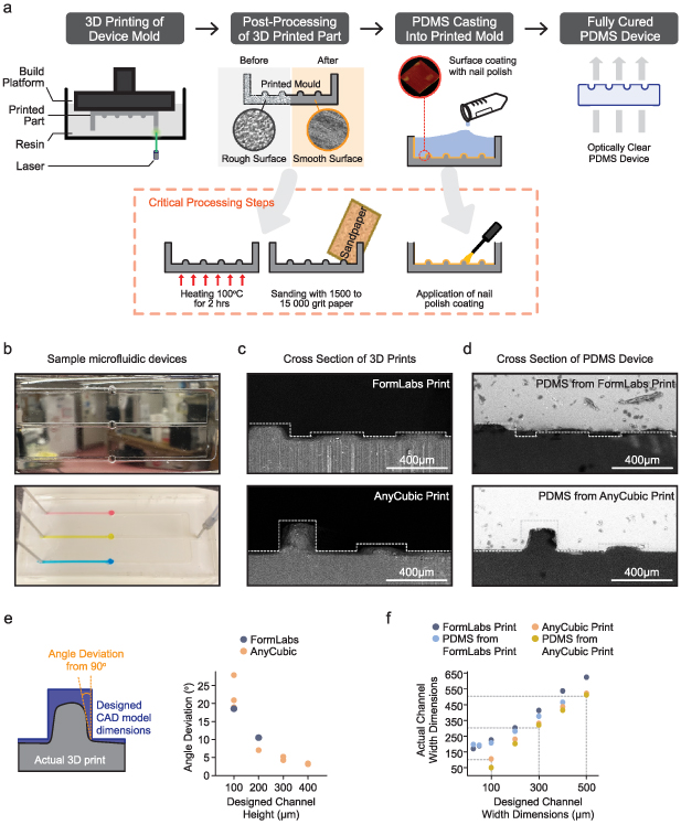
Figure 1. Commercial 3D printing is a power tool in the fabrication of PDMS microfluidic devices. (a) Outline of the fabrication and post-processing method. Master moulds were 3D printed using the Formlabs Form 3B using clear resin or the Anycubic D2 DLP using black resin. Three-dimensional printed parts were post-processed, which involves critical steps including heat treatment, physical sanding, and chemical coating with nail polish. These post-processed moulds were used to cure PDMS, resulting in a fully cured, optically clear microfluidic device. (b) Sample images of the microfluidic device (top) adhered to a glass microscope slide using double-sided medical-grade tape and (bottom) to the double-sided tape alone with dyed distilled water flowing through. Cross sections of the (c) 3D printed mould or (d) the resulting PDMS device were imaged using a scanning electron microscope. Dotted lines represent the theoretical feature that should have been printed and was designed in the CAD software. (e) Measurements of the angle between the hypothetical feature (channel wall) and the actual printed channel wall, as a proxy for accuracy of the 3D printed mould, for both FormLabs and AnyCubic printed parts. (f) Measurements of the channel features that resolved on the 3D printed mould compared to the designed width dimensions in the CAD file. Dotted grey lines are a reference for perfect printing; features that printed the same dimension as initially designed.
Download figure:
Standard image High-resolution imageNext, we sought to determine the accuracy of the commercial SLA printers in printing the CAD-designed moulds, and how well this translated to the final PDMS device. SEM imaging of positive moulds and PDMS devices generated by FormLabs and AnyCubic printers confirmed that the designed channel features could be resolved (figures 1(c) and (d)). Notably, both commercial printers could create channel heights as low as 100 µm, with the FormLabs capable of going as low as 50 µm (figure 1(c)). However, at <100 µm the channel features were less resolved, and both the 3D print and resultant PDMS device did not form sharp, distinct walls and instead were slanted (figures 1(c) and (d)). To quantify this, we measured the angle between the channel wall and a theoretical plane perpendicular to the printed surface, which would otherwise be a perfect wall if the printer replicated the CAD design perfectly (figure 1(e)). Indeed, we found that only the designed channel heights >200 µm resulted in more accurately printed channel walls (<10 degrees deviation) (figure 1(e)). In the XY plane, we found that the AnyCubic printer was able to accurately fabricate the desired channel widths. Surprisingly, the FormLabs printer consistently created channel widths that were ∼100 µm greater than the CAD design (figure 1(f)), a factor that must be considered in 3D design. Nevertheless, with proper 3D design and an understanding of the limitations of each printing method, we showed that commercial 3D printing can certainly be used in the design and fabrication of PDMS microfluidic devices.
3.2. Heat treatment of 3D printed moulds is required for proper curing of PDMS
We observed a significant amount of PDMS curing inhibition at the interface between the PDMS surface and the 3D printed surface, which has been previously reported in applications involving 3D printed moulds (figure 2). The resultant PDMS did not fully cure, leaving behind a sticky texture with many channel features failing to form, or being formed at very low resolution. To relieve this inhibition, we treated our printed moulds with high heat at 100 °C for up to four hours. This resulted in a completely cured and translucent PDMS surface, through manual observation and brightfield microscopy (figure 2). Notably, the surface of the device was smooth, and the device features were properly formed. We found that longer heat treatments resulted in increased PDMS curation, as evident by an improved PDMS surface texture and perfect channel edges. Importantly, at extremely high temperatures (∼120 °C) or prolonged heating (>8 h), the 3D printed moulds warped and/or cracked, decreasing the likelihood of generating PDMS microfluidic devices with accurate channel dimensions (data not shown). Overall, 3D prints acquired from SLA printers require high heat treatment to allow complete PDMS curing.
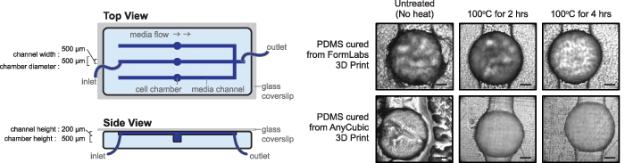
Figure 2. Heat processing is required for complete PDMS curing in 3D printed moulds. (Left) A schematic representation of PDMS device, with arrows indicated the direction of media flow through the channels and chambers within the device. (Right) Brightfield microscopic images of PDMS obtained after removal from the 3D printed mould that was subjected to varying high heat treatment durations. Scale bars indicate 100 µm.
Download figure:
Standard image High-resolution image3.3. Post-processing of 3D printed moulds is required for generating smooth PDMS surfaces
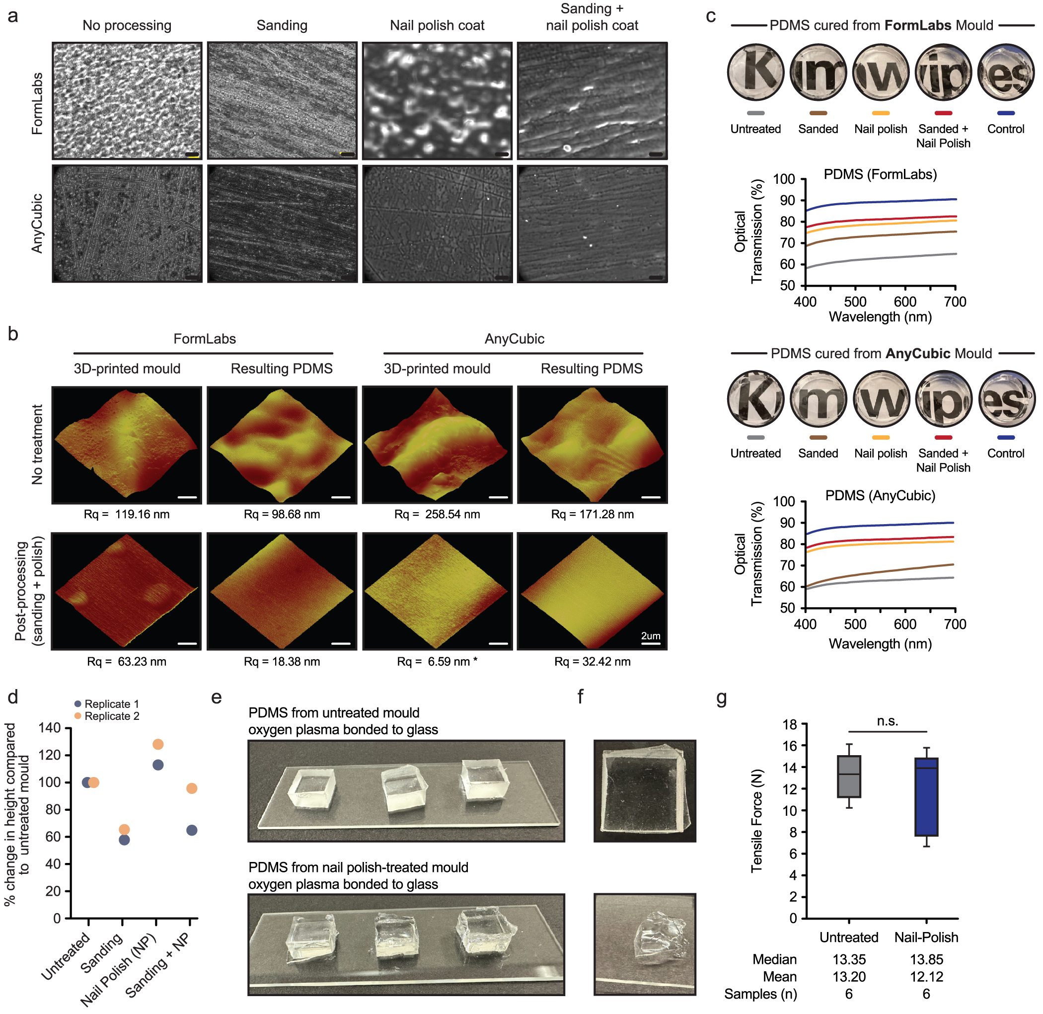
Despite the successful fabrication of a PDMS microfluidic device, the resultant PDMS devices were optically translucent, likely due to the surface roughness of the 3D printed moulds. The PDMS surface was textured and not clear microscopically (figure 2). Furthermore, when visualizing the surface of the PDMS devices obtained using these moulds by brightfield microscopy at higher magnification (63X magnification), it was immediately clear that the surface was uneven and rough (figure 3(a)). The surface contained various imperfections, such as streaks and ridges. Therefore, we sought to design an inexpensive and simple post-processing method that would dramatically reduce the surface roughness of our 3D prints, ideally translating to the PDMS device. Ultimately, our goal was to reduce surface roughness and imperfections on the PDMS device itself, as this is a critical requirement for optical clarity. We opted to sand the features of the 3D moulds with increasing grit sandpaper, from 1500 to 15 000 grit, to remove large debris and imperfections in the 3D print, which resulted in a visually smoother surface but left streaks and scratches (figure 3(a)). Therefore, with sanding alone, the resulting PDMS devices were translucent and conformed to the scratches visible on the moulds. Polishing and applying chemical-based coatings, such as spray painting and lacquer coatings, as a final surface finish have been described [28]. We explored several chemical coating methods, including silicon-based sprays (mould release spray), polyvinyl alcohol, and polyurethane, all of which inhibited PDMS curation. However, we also assessed the ability of NP, an extremely common coating agent that is readily available, to smoothen the surface of the moulds. We noted that heat-treated and NP coated 3D printed moulds can reduce the surface roughness and significantly reduce the visible surface roughness when combined with the initial sanding of the 3D print (figure 3(a)). Both post-processing steps reduced the surface roughness of the 3D print by almost two-fold (Rq from 119.16 to 63.23; figure 3(b)) and were suitable to cure PDMS.
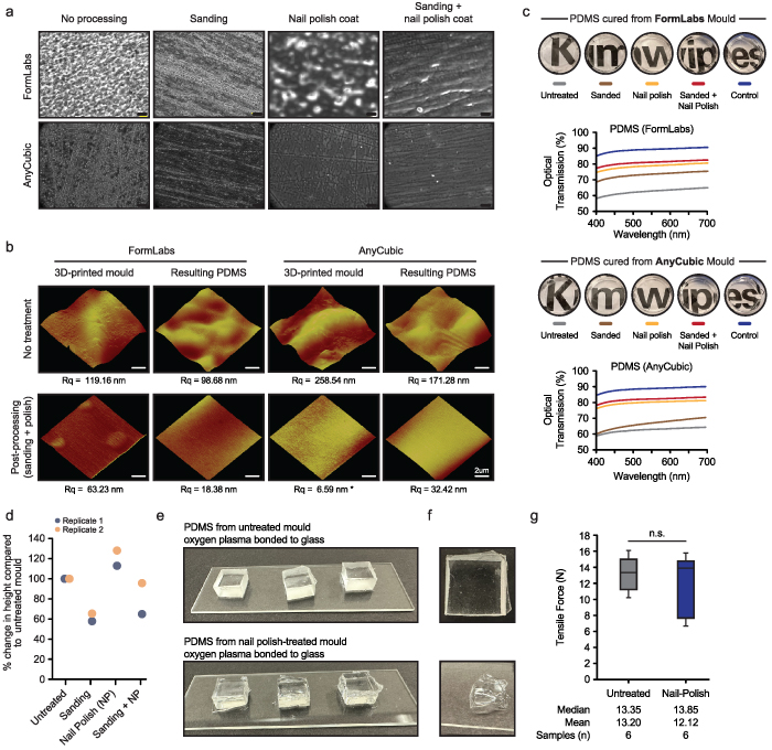
Figure 3. Sanding and chemical coating of the 3D print generates an smoother surface that results in optically clear PDMS devices (a) brightfield images of PDMS surfaces obtained from FormLabs and AnyCubic 3D printed moulds after post processing steps. Scale bars represent 50 µm. (b) Three-dimensional AFM image of both the 3D printed surface and the PDMS surface obtained from each respective mould. The root mean square roughness (Rq) for each surface is indicated below the image. (c) Circular PDMS cut-outs were obtained from 3D printed moulds, either post-processed or not, and the optical transmission (%) was calculated and plotted for both FormLabs- and AnyCubic-derived PDMS surfaces. (d) The height of channel features on FormLabs 3D printed moulds was measured for each condition/treatment. The measurements were normalized to the height of the untreated mould. (e) Square PDMS cut-outs (1 cm × 1 cm × 1 cm, lwh) were generated from 3D printed moulds, with or without nail polish treatment, and oxygen plasma bonded to glass slides. (f) Top-view of PDMS plasma bonded to glass (top) and an image of residual PDMS material still remaining after force was applied to remove PDMS from glass slide (bottom). (g) The tensile force applied to remove PDMS from the glass slide was recorded using a spring scale. Median, mean, and number of samples are indicated below.
Download figure:
Standard image High-resolution imageNext, we used atomic force microscopy (AFM) to obtain higher resolution images, and quantified the root mean square roughness (Rq) of the 3D printed moulds and resulting PDMS surfaces. Interestingly, PDMS devices fabricated from moulds that had not undergone post-processing exhibited lower surface roughness than its mould counterpart (FormLabs: Rq from ∼119 to 99 nm; AnyCubic: Rq from ∼259 to 171 nm). However, with post-processed moulds, there was an extreme reduction in surface roughness of the resulting PDMS device in all cases when compared to the non-processed PDMS device (FormLabs: Rq from ∼63 to 18 nm; AnyCubic: PDMS device with Rq ∼ 32.42 nm). We note that in all technical replicates of the AnyCubic 3D printed mould, we could not get reliable estimates of the surface roughness. Nevertheless, the resulting PDMS surface obtained from the moulds from both commercial printers was >5-fold smoother than PDMS obtained from an untreated mould.
The resultant PDMS surfaces obtained through post-processing exhibited greater clarity, visibly, compared to the non-processed counterpart (figure 3(c)). This was further validated when we assessed the optical transmittance (a measure of clarity) of various post-processed PDMS samples, within the 400–700 nm range, compared to a control PDMS surface cured in a glass mould. We found that PDMS surfaces originating from moulds that were post-processed with both mechanical sanding and NP coating resulted in the highest level of transmission (78%–83%) across scanned wavelengths compared to the non-processed moulds and approached the transmission of the control PDMS surface, which exhibited transmission levels of 85%–89% (figure 3(c)). Notably, the clarity of PDMS surfaces from moulds treated with only a NP coating was still quite high (75%–81%). This suggests that this coating is the main factor for PDMS surface smoothness and clarity, with mechanical sanding responsible for increasing clarity by ∼2%–3%, likely due to the removal of larger surface debris and imperfections. It should be noted that we observed that physical sanding can cause up to 50% removal of resin material that form our microfluidic features, which is approximately ∼40 µm change in height in our devices (figure 3(d)). Additionally, the application of NP was observed to add ∼11 µm of height in our devices (figure 3(d)). These two factors must be a consideration when performing these post-processing steps. Future work will expand on these methods to limit the amount of 3D printed material that is lost from sanding and optimizing the NP coating to minimize the additional material added to our master mould. Nevertheless, our data outline the importance of the post-processing of 3D printing moulds to generate optically clear PDMS devices.
One other potential issue with rough PDMS surfaces is its ability to be bonded to glass surfaces using oxygen plasma. A smoother surface could facilitate greater PDMS-glass bonding. To investigate this, we oxygen plasma bonded PDMS (1 cm × 1 cm × 1 cm cut outs) from moulds produced using the FormLabs printer, with and without NP treatment (figure 3(e)). Surprisingly, we find that our PDMS substrates, regardless of NP treatment, is capable of bonding to glass tightly. When a tensile stress was applied, commonly, the PDMS substrate would break internally before its bond with glass was broken (figure 3(f)). The tensile force required to cause the PDMS or PDMS-glass bond was on average 13.20 and 12.12 Newtons for substrates generated from untreated and NP-treated moulds, respectively (figure 3(g)). This is equates to 0.1320 and 0.1212 Megapascals, which is at least within an order of magnitude and corroborates other reported values [29, 30]. Therefore, PDMS surfaces derived from FormLabs-based master moulds can be oxygen plasma bonded, though a smoother surface may facilitate more even bonding through the microfluidic device.
3.4. PDA- and collagen-coated PDMS devices have greater surface hydrophilicity
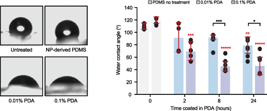
Despite being highly biocompatible, PDMS is also highly hydrophobic, which can pose significant complications for microfluidic devices intended for cell-based applications. Therefore, we applied a chemical surface modification (previously reported to increase surface hydrophilicity) using PDA [31, 32]. PDMS substrates were coated with various concentrations of PDA for 2, 8, or 24 h, and the WCA was measured as a proxy for surface hydrophilicity. PDA-coated devices coated exhibited significantly reduced WCA compared to non-coated PDMS surfaces (figure 4). Notably, this effect was concentration dependent as the surfaces coated with 0.1% PDA had a smaller WCA than the surfaces coated with 0.01% PDA. Therefore, the resultant PDMS microfluidic devices fabricated using our method can be modified similarly to those reported in the literature to produce hydrophilic surfaces that are suitable for cell culture applications.
Figure 4. Polydopamine-coated PDMS significantly increase surface hydrophilicity. (Left) Representative images of water droplets on PDMS surfaces are shown, with or without incubation in 0.1% or 0.01% dopamine hydrochloride solution at pH 8.0. (Right) The mean contact angle of PDMS coated with 0.1% or 0.01% polydopamine is plotted for 0, 2, 8, and 24 h of incubation in the coating solution. Error bars represent ± one standard deviation. Statistical analysis was performed using the Tukey honestly significant difference (HSD) test: *p-value < 0.05, **p-value < 0.01, ***p-value < 0.001, *****p-value < 0.000 01 (n > 3).
Download figure:
Standard image High-resolution image
4. Discussion
PDMS microfluidic devices are extremely attractive for its capabilities to reduce in reagent consumption, increase scalability, and the ability to create unique designs has greatly innovated cellular research, particularly in precision medicine and high-throughput drug screening [9, 11, 33–35]. Despite all these advantages, microfluidic systems have not been widely adopted by biology researchers [36]. Several factors can be attributed to the gap between researchers and the use of microfluidic devices, including: (1) fabrication and (2) use of the device [37]. The fabrication process often requires specialized and expensive equipment, and the operation of microfluidic devices can be difficult and cumbersome for the user; both deterring the setup and use of microfluidic systems in biology research. To address the first obstacle, our work outlines an inexpensive and simple approach to rapidly generate optically clear PDMS microfluidic devices that can have extensive biological.
4.1. Commercial SLA 3D printers are useful tools in PDMS device fabrication
3D printing technologies have made great strides in biomedical and biomolecular research [5, 6, 17, 38, 39]. Though 3D printing has been used in the fabrication of PDMS microfluidic devices, its use remains limited. We aimed to provide a detailed guideline for the fabrication of PDMS devices using 3D printing technology. Our focus was to construct a simple and versatile method to generate PDMS microfluidic devices, from start to finish, with a product suitable for mammalian cell applications. We pushed the limits of the available FormLabs and AnyCubic 3D printers and showed that we could generate channel features in the <100 µm range, though larger feature sizes result in a more accurate final product. We were able to generate devices with small features (>25 µm channel height) that were still capable of fluid flow. This is, to the best of our knowledge, the lowest reported PDMS structure generated with 3D printing. Future developments in the field of 3D printing will maximize the resolution limit while maintaining the accuracy of the final printed part.
4.2. Post-processing of 3D moulds is critical for optically-clear devices
The potential applications for PDMS microfluidics are vast, spanning from diagnostic systems to sample testing and drug discovery [3, 8, 40, 41]. To date, 3D printing has not yet produced PDMS microfluidic devices with the same level of resolution and clarity when compared to devices obtained from more traditional methods. This is largely due to the limitations of the printer, PDMS curing inhibition that may result from different types of photocurable commercial resins and the smoothness of the resulting moulds that are generated by 3D printing. Our described post-processing steps can be applied in a wide range of laboratory settings, producing clear PDMS devices that approach those created via photolithographic techniques.
The first critical component of our post-processing step is the heat treatment of the 3D print. Contingent on the type of resin used, most photocurable resins are comprised of acrylate monomers, crosslinkers, colouring agents/photo absorbers, plasticizers, and most importantly, the photo initiator. Phosphine-oxide-based photo initiator fragments can leach from the moulds and inhibit the PDMS catalyst [42, 43]. In contrast, unreacted monomers strongly bind and attach PDMS to the 3D-printed surface. Both photo initiator and unreacted monomers can remain even after the 3D printing process, and their combined actions result in PDMS curing inhibition. UV treatment maximizes the polymerization of the resin and high-temperature treatment of the moulds allows any present photo initiator to be vapourized, both processes reducing the presence of residual photo initiator and resin monomer, enabling proper PDMS curing [44]. In line with these studies, we found that high heat treatment enables complete and proper PDMS curation. Notably, moulds are susceptible to cracking and breaking at prolonged levels of dry heating at >100 °C, so we propose the use of shorter heat treatments or high heat treatment with humidity (such as the autoclave), which does not visibly affect the structural integrity of the mould.
The second important post-processing step involves physical and chemical surface modifications to the 3D print to obtain a smooth surface. Several spray paint or lacquer coatings have previously been used to conceal the layer markings of 3D printed objects [28]. Similarly, chemical coats with SU-8 and fluorosilanes have been used to improve PDMS curing and clarity [14]. Furthermore, Parylene-C coatings have also been used to aid in PDMS release in addition to protecting master moulds, extending the number of cycles of moulding with various polymers [45, 46]. However, these methods require specialized pre-treatments, equipment, and/or deposition methods. We provide an alternative, low-cost coating solution involving NP, which significantly increases the surface smoothness of the 3D printed moulds, resulting in extremely clear PDMS surfaces (Rq < 33 nm). In comparison, the surface roughness of Pyrex glass has been estimated to be Rq = ∼1 nm [47]. Although our fabrication method does not produce PDMS surfaces rivalling that of pure glass substrates, we outline a novel post-processing method that approaches the surface smoothness of glass and outperforms other reported methods that use 3D printing to generate PDMS devices [48, 49].
The final part of our post-processing outline involves the application of a coating to the PDMS surface to increase hydrophilicity. PDMS is a highly hydrophobic substrate. This is particularly problematic for cell biological applications since adherent mammalian cells will not adhere to a hydrophobic surface [1, 10, 50, 51]. Additionally, air bubbles can readily form within a hydrophobic microfluidic device as hydrophilic media or solutions are flowed through the device [52]. Therefore, increasing the hydrophilicity of the PDMS surface allows for biomedical applications and promotes proper operation of the microfluidic device.
5. Conclusion
The use of photo-polymerization methods to generate master moulds and create microfluidic devices is an emerging field that is beginning to bring microfluidic capabilities and experimentation to researchers, even those that lack specialized microfluidic equipment. Since this field is still in its early stages, recent work, including our own, has been aimed to characterize these fabrication methods and provide guidelines to generate simple, efficient, and inexpensive devices [16]. As advancements in 3D printing technologies continue to push the resolution limit, we anticipate that our post-processing steps will remain a highly efficient and inexpensive method to produce highly transparent and functional PDMS devices.
Acknowledgments
This project was supported and funded by Mitacs (through the Mitacs Accelerate program), InnoHK initiative and the Hong Kong Special Administrative Region Government, the Canadian Optometric Education Fund (COETF), and the Centre for Bioengineering and Biotechnology (CBB) at the University of Waterloo. We thank WATLab at the University of Waterloo for assistance with acquiring SEM and AFM images. The University of Waterloo acknowledges that much of our work takes place on the traditional territory of the Neutral, Anishinaabeg and Haudenosaunee peoples. Our main campus is situated on the Haldimand Tract, the land granted to the Six Nations that includes six miles on each side of the Grand River. Our active work toward reconciliation takes place across our campuses through research, learning, teaching, and community building, and is coordinated within the Office of Indigenous Relations.
Data availability statement
All data that support the findings of this study are included within the article (and any supplementary files).
Author contributions
Conceptualization, N Q, C M P, C R and L J; Methodology, B H, N Q, and C M P; Post-processing of 3D printing, B H and C M P; Experimentation, M R and B H; Water Contact Angle, M R; Scanning Electron Microscopy, M R and B H; Atomic Force Microscopy, M R; Optical Transmission, M R; Brightfield Microscopy, M R and B H; Formal Analysis, B H and M R; Writing—Review & Editing, B H, C M P, and L J.
Conflict of interest
The authors declare no conflict of interest.