
Abstract
Parylene C is a commonly used polymer in the micro-electromechanical systems (MEMS) field because of its excellent barrier property and process compatibility with other microfabrications. Whereas, the poor adhesion of other materials to Parylene C is the urgent challenge that restricts its real applications. This work proposed a strategy to enhance the adhesion between Parylene C or metals and the Parylene C substrate. A short-time oxygen plasma reaction ion etching process with ambient titanium in the etching chamber is introduced between the first layer of Parylene C film deposition (the substrate) and the second Parylene C or metal coatings. Parylene C nanostructures (nanograss) are generated on the substrate because of the oxygen plasma bombarding with sputtered titanium nanoparticles as nanomasks. Different feature sizes of nanograss were successfully obtained by tuning the RF power, oxygen flow rate and etching times. Scanning electron microscopy images showed that both the nanograss density and height (0.61 ± 0.02 μm–0.76 ± 0.03 μm) were positively proportional to the etching time with low RF power (150 W) and oxygen flowrates (60 sscm). Scratch tests are conducted after the second layer of Parylene C or metal coatings to quantitively analyze the adhesion enhancement. The results indicated that the adhesion of both Parylene C and metal on the Parylene C substrate with nanograss structures were enhanced up to around 7 and 15 times, respectively, compared to those on untreated substrates. This nanograss technique-based adhesion enhancement approach is easy-to-realize, robust, chemical-free, precisely controllable, thereby holds promising potentials in various Parylene MEMS applications.
Export citation and abstract BibTeX RIS

Original content from this work may be used under the terms of the Creative Commons Attribution 4.0 license. Any further distribution of this work must maintain attribution to the author(s) and the title of the work, journal citation and DOI.
1. Introduction
Parylene has been used for more than 50 years in electronics, biomedical industry, aerospace, among others. The perfect barrier property, bio-compatibility and capability of realizing thickness at sub-microns enabled Parylene acting as encapsulation layer in various fields [1–4].
Among all the Parylene variants, Parylene C is the most commonly used due to its manufacturing advantages and biocompatibility. micro-electromechanical systems (MEMS) device with Parylene C as encapsulation layer especially for the in-vivo applications are developed because of the demanding of unique properties [2, 5]. The conformal and pinhole free coating behavior under room-temperature enabled Parylene C coatings to be the best choice than other polymers or coating materials.
Despite of the mentioned usage of Parylene C in MEMS, the inherent limitations still significantly hampered Parylene C from applicating in microfabrications while the poor adhesion between Parylene C and other materials shows the most severe restrictions. Poor adhesion of Parylene C restricted it in undergoing wetting process like KOH etching [6, 7]. The long-term application in fluidic environment is also limited as the delamination of Parylene C [8, 9].
There are various methods raised to solve the adhesion problems and they can be classified into two strategies, (a) chemical approaches by introducing interlayer or modifying film surface with chemicals [10–13]; (b) surface roughness or mechanical structures to enlarge the surface/volume ratio [11, 14]. The commonly used chemical approach is coating adhesion promoter like A-174 between Parylene C and others. While, the effectiveness of A-174 is limited by the thermal budget [10]. Molten Parylene C and molten Parylene C acting as adhesion layer also present distinct increase in adhesion [7, 11]. The molten Parylene C however showed clear change in phase and crystallinity resulting alterations in surface properties. The mechanical methods on the other hand can maintain the chemical stability and will not cause potential harm from new materials. Additional structures are often generated on the surface to increase surface/volume ratio. XeF2 etching are conducted by Huang et al to roughen the surface and anchoring structure is further fabricated by deep reactive ion etching to realize interlocking structures [11].
Notable factor is that most researchers are focusing on Parylene on Si or metal, while few investigate the adhesion when Parylene acting as substrate layer. Tai et al experimented some techniques to promote Parylene–Parylene adhesion [12]. Hexane, toluene and Propylene carbonate are span to work as interlayer. CF4 plasma etching then roughened the Parylene C surface to achieve mechanical enhancement.
Whereas, the chemical approaches are lack of universal applicability as the extra materials may hamper the process-compatibility due to containment. Surface roughening increased the exposed area whereas the surface/volume ratio increase is not the determining factor in CF4 plasma etching and the fluorine groups added increased the adhesion as polar mechanism indicate.
Here we proposed a technique to enhance adhesion for Parylene C or metals depositing on Parylene C substrate. A short-time oxygen plasma reaction ion etching (RIE) process with ambient titanium in the etching chamber is introduced between the first layer of Parylene C film deposition and the second Parylene C or metal coatings. Parylene C nanostructures (nanograss) are generated on the Parylene C substrate because of the oxygen plasma bombarding with sputtered nanoparticles as nanomasks. Parameters including Radio Frequency (RF) power, oxygen plasma flowrate and etching times in RIE process are exanimated to tune the feature size of nanograss. Scratch tests are conducted to quantitively analyze the adhesion strength.
2. Experiments and methods
2.1. Principles of nanograss generation
Surfactant coated silicon wafers are used as the substrate for Parylene C deposition with purpose to easily separate the Parylene C to Parylene C (P-P) and Parylene C to metal (P-M) bilayer structures. The Parylene C deposition is carried by commercial SCS PDS2010 deposition equipment. The substrate layer of Parylene C is deposited on the samples.
The fabrication process of the nanograss structure is shown in figure 1. After the preparation of Parylene C substrate along with titanium (Ti) mask on top, oxygen plasma etching was performed in an RIE chamber. During the oxygen plasma etching, the Ti nanoparticles are sputtered off from the mask and deposited onto the Parylene C film and formed micro-masks. The Ti micro-masks protected the local Parylene C from being etched off. Eventually, Parylene C structures similar to grass in nature, which called 'nanograss' here, were obtained on top of the Parylene C film [15–17].

Figure 1. Fabrication process of the nanograss structure.
Download figure:
Standard image High-resolution image2.2. Samples preparation
The adhesion testing samples for scratch test [18, 19] were evaluated and compared after being subjected to the following conditions (figure 2):
- (a)No treatment
- (b)Parylene C nanograss by oxygen plasma etching
- (c)A174 coating before Parylene C nanograss preparation (Pre-A174)
- (d)A174 coating after Parylene C nanograss preparation (Post-A174).
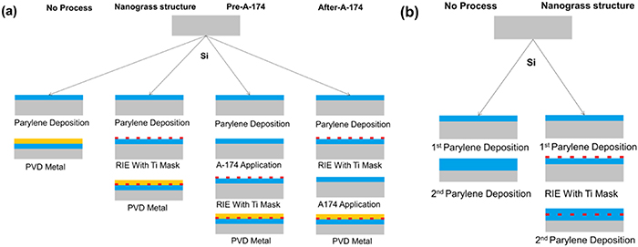
Figure 2. Microfabrications of Parylene C with different treatments. (a) Treatments for interface of P-M. (b) Treatments for interface of P-P.
Download figure:
Standard image High-resolution imageP-M samples were sputtered with 100 nm Ti and 1 μm copper (Cu) by physical vapor deposition (PVD) while the P-P samples were deposited with 3 μm Parylene C after treated by the above conditions.
2.3. Scratch test
Interfacial adhesion between the P-P and P-M were measured using Keysight G200 nano-scratch tester in ambient air, at the temperature of 25 °C and a humidity of 20% [18–20]. At least three samples for each condition and three scratches were carried on each sample. The lateral forces were recorded and defined as the detachment point when the scratching indenter reached the interface between two layers. Then the lateral forces were used to describe the adhesion between two layers.
3. Results and discussion
3.1. Tuning of etching recipes
Parameters of RIE process influenced the feature size of nanograss (height, density). The results of tuning RF power and flowrate of O2 are presented in figure 3 where scanning electron microscopy (SEM) images are displayed to compare the feature size of nanograss. Three different RF power values (150 W, 250 W, 350 W) are experimented with O2 flowrate and etch time fixed at 60 sccm and 300 s, respectively. Different RF power values inducing nanograss displayed rather similar feature size and density, thereby low RF power 150 W is selected for the nanograss preparation.

Figure 3. SEM images of the nanograss structures. (a) RF power affected nanograss and (b) flowrate affected nanograss. (c) Nanograss with variable etching cycles.
Download figure:
Standard image High-resolution imageThe results of different flowrate of O2 plasma are also presented in figure 3(b), where flowrates at 45, 60 and 90 sccm are compared. The RF power is set at 150 W and all the samples are etched for 300 s. The nanograss structures presented similarity in both size and density. However, the low flowrate, 45 sccm, is not stable for long-term etching because the pressure in chamber is below the floor level of the equipment. Therefore, the parameters of RIE process are determined at 150 W for RF power and 60 sccm for O2 flowrate.
The etch times are investigated after the RF power and O2 flowrate are determined. Different etch times are compared on the nanograss feature sizes. Etching for 75 s with RF power at 150 W and O2 flowrate at 60 sccm is defined as one cycle and the etching times ranged from 1 to 4 cycles. The results for different cycles are presented in figure 3(c). Nanograss generated for samples underwent one cycle of etching and the nanograss become higher for more cycles (0.61 ± 0.02 μm–0.76 ± 0.03 μm). However, the density of nanograss decreased as the etching cycles increases while the height become larger. Therefore, both density and height of nanograss are capable of tuning by etching cycles (times).
3.2. Scratch test results
3.2.1. Etching cycles.
Figure 4 displayed the interfacial adhesion results of P-M and P-P samples with different etch cycles. Fabrication and testing conditions, except of etch cycles, were remained the same for the test samples to eliminate influence from other factors like the surface roughness and the sample thickness. Untreated samples exhibited very small adhesion strength with test results for P-M and P-P were only 0.75 ± 0.18 mN and 3.27 ± 1.0 mN, respectively. Different etch cycles lead to different interfacial adhesion strengths. The samples with nanograss structures showed maximum 7.3 (P-M) and 15.2 (P-P) times enhancement of adhesion strength compared with the untreated ones. The maximum adhesion strength of P-M arose after two cycles of etching (5.45 ± 0.4 mN) and the highest adhesion strength of P-P was obtained after three cycles of etching (49.93 ± 7.13 mN). Another method to evaluate the adhesion strength is via the work of adhesion, and contact angle is a measurable method to quantify the work of adhesion [21, 22]. Generally, larger contact angle indicates smaller work of adhesion, i.e. a smaller adhesion strength. An optical contact angle test was conducted to validate the adhesion enhancement. The contact angle dropped from 95° for the untreated Parylene C film to 82° for the Paryene C film with nanograss structures. The decreased contact angle indicated an increment of adhesion strength when nanograss was generated on top of Parylene C films. Besides the above analysis of the work of adhesion, nanograss was also an interlocking structure. During the PVD process of metal and Chemical Vapour Deposition (CVD) process of Parylene C, micro-molecules/atoms penetrated into the voids of the nanograss and eventually formed mechanical interlocking structures. The interlocking structures were able to increase the adhesion strength as the contact surface area between two layers increased dramatically. As shown in figure 3, the exposed surface area of nanograss was not linearly related to the etch cycle as more etch cycles led to sparser and higher nanograss structures. The maximum enhancement of the adhesion strength for both P-M and P-P samples did not obtained at the largest etch cycle (the 4th etch cycle), but at 2nd for P-M and 3rd for P-P, which was consistent with the contact surface area related mechanism of interlocking enabled adhesion enhancement [21–24]. Moreover, the different etch cycle for the maximum adhesion strengths of P-P and P-M mainly due the different penetration capabilities of different coating materials and processes. The metals deposited by the PVD process is carried out at an extremely higher chamber vacuum (∼10−6 Pa) compared to the CVD process of Parylene C (∼1 Pa). Moreover, the diameter of the metal atoms is significantly smaller than Parylene C molecular. These two factors jointly contributed to the larger mean free path of metal atoms, thereby presented higher penetration capability into the narrow but deep nanograss structures to form more firm interlocking structures. Therefore, maximum adhesion strength was realized with smaller etch cycle of P-M samples.
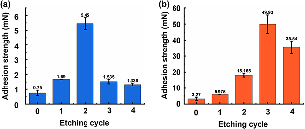
Figure 4. Interfacial adhesion results as a function of different etching cycles. (a) P-M and (b) P-P.
Download figure:
Standard image High-resolution image3.2.2. Adhesion promoter A174 assisting nanograss.
Adhesion results with A174 coating are presented in figure 5. A174 was coated before and after oxygen plasma etching with Ti sheets inside the chamber for 75 s. The interfacial adhesion without A174 was 1.69 ± 0.014 mN while after A174 coating the Pre-A174 and Post-A174 adhesions were increased to 3.795 ± 0.3 mN and 4.145 ± 0.2 mN, respectively. This indicated that both before or after the oxygen plasma etching, the adhesion of P-M was enhanced with A174 coating. The mechanism of A174 to enhance the adhesion was because A174 can act as a 'molecular bridge' connecting Parylene C and metal (Cu), formed a Parylene C-A174-metal bonding structures, which further enhances the adhesion strength of the nanograss structure to metal. [1, 25] Pre-A174 was structured after the coating of A174, the RIE treatment etched part of A174 and reduced the bonding structures when coating the metals. Thus, the enhancement of adhesion strength of Pre-A174 was smaller than that of Post-A174.

Figure 5. Interfacial adhesion results with A174 coating.
Download figure:
Standard image High-resolution image
4. Conclusions
Here we proposed a nanograss based technique to enhance adhesion between Parylene C substrate and Parylene C or metal coatings. The adhesion improvements are quantitively investigated by a scratch test. The nanograss assisted samples showed up to ten times improvement compared with the untreated ones (0.75 ± 0.18 mN to 5.45 ± 0.4 mN for metal to Parylene C and 3.27 ± 1.0 mN to 49.93 ± 7.13 mN for Parylene C to Parylene C). This nanograss technique-based adhesion enhancement approach is easy-to-realize, robust, chemical-free, precisely controllable, thereby holds promising potentials in various Parylene MEMS applications.
Acknowledgments
We are grateful for the supports from National Key R&D Program of China(2017YFA0206003) and National Natural Science Foundation of China (Grant Nos. 62074003, 82027805). This work is supported by the 111 Project (B18001).
Data availability statement
All data that support the findings of this study are included within the article (and any supplementary files).